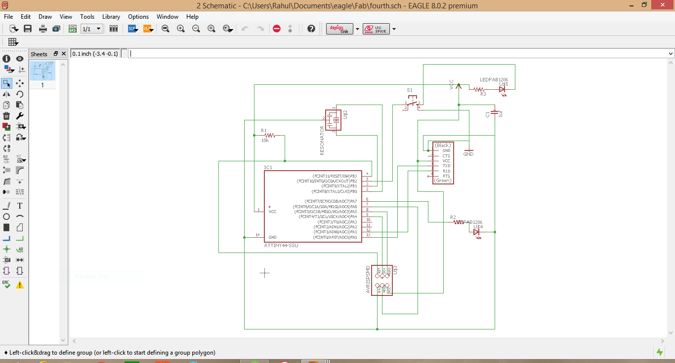
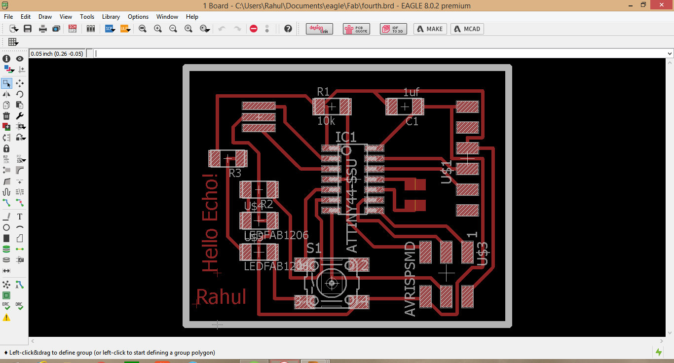
During the electronics design week, I had designed a board based on Neil's Echo Hello board. I had added a switch to PB2 and two extra LEDs, one connected to power and the other connected to PA7 of my board. In order to test the board, with the help of our instructors, I flashed the Echo Hello program on my board that week and tested it to make sure that the board was working. I also used arduino IDE to blink the LED on my board. Both the programs ran successfully. I have documented the steps I followed to program the board on week 6
I'm from a Mechanical background hence this is all new for me, most of the time this week i was running around the lab like a headless chicken not knowing what to do. All the terms were new to me. I understand that the first thing I must do is to understand the cip I'm programming. This meant that I have to start with the Data sheet for the ATtiny44. I searched online and found the data sheet for the ATtiny44A
The Datasheet has a lot of information about the chip like the pinout configuration, the different registers and timers that are available in the chip and how you can access them.You will easily get overwhelmed by the vast amount of information. The user friendliness of the data sheet is very limited, a lot of the terms used in it are unfamiliar to me.

Attiny 44A is the high performance 8bit AVR RISC based architecture microcontroller by Microchip It is having 4KB ISP flash memory,256 Byte EEPROM, 256B SRAM,12 general purpose I/O lines, 32 general purpose registers,an 8 bit timer/counter with two PWM channels,a 16-bit timer/counter with two PWM channels, internal and external interrupts, an 8-channel 10-bit A/D converter, programmable gain stage (1x, 20x) for 12 differential ADC channel pairs, programmable watchdog timer with internal oscillator, internal calibrated oscillator, and four software selectable power saving modes. The device operates between 1.8-5.5 volts. More detailed about each is described in the datasheet of ATtiny44A
From the pinout diagram you can see that there are two ports on this chip. PORT A and PORT B. Port A has 8 pins and Port B has 4 pins. All these pins are general input output pins. which you can use to control external components.
The first place to start would be some AVR Tutorials

DDRx DDR stands for Data direction Register, basically it is an 8-bit register which determines whether one pin will be an input or output pin. If you want the pin you connected the LED to be set as output then you should give that value of that as 1 on DDRx. Example I connected my LED to PA7, hence I have to make it as out put in DDRA.
Hence I give the code to set the pin PA7 as out put by writing. DDRA=0xff; This is HEX equivalent for DDRA=ob11111111 What this does is that it will set all the pins on the PA7 as output pins.
PORTx while DDRx denotes the direction of the Pin, PORT denotes the state of it. That means if I give a value 1 in the PORT register of that pin It would be set to HIGH, or 5V in case of the micro controller.
PINxPIN register is a dynamic register whose value will be automatically updated based on the received values of the sate of all pins, so 5V to that pin will write 1 to that register.
When we want to write values into the Port register, we intent to change specific values in the register while leaving the rest untouched. A way to do that is by using a Masking variable.
A Masking variable is a variable of the same length of data you are comparing, it allows you to extract specific number of bits out of the entire line of data.
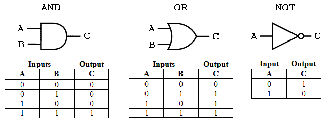
To do this you need to have an understanding of logic gates and how they work. The 3 basic logic gates are AND, OR, NOT.
Suppose I've connected my LED to PB0 and want to turn it on without disturbing the other values. Here's how to do it.
	PORTB xxxxxx10 //We want to set PBO as one, without affecting the other values.
		OR
	      00000001 // Masking variable
	................
       PORTB xxxxxx11 //Result
Let the other values in the register be x, we don't want to change that. Using the OR operation we have successfully changed the value of PBO to one. IN the OR operation putting the value 0 will not change the original value.The program equivalent of that is
PORTB|=0x01; // read as PORTB or equal to 0x01
Now suppose you want to turn that bit OFF, how would you do that? You cannot use the OR operation turn turn a 1 to a 0. The way you do that is by using the AND operation.
	PORTB xxxxxx11 //We want to set PBO as zero, without affecting the other values.
		AND
	      11111110 // Masking variable
	................
       PORTB xxxxxx10 //Result
In the AND operation 1 is the Protecting Bit and 0 is the destroying bit. So wherever you want to change the value to zero give that value as zero in the masking variable. The program equivalent is
PORTB&=0xFE; // read as PORTB AND equal to 0xFE. The binary of 0xFE is ob11111110
C language was developed by Dennis Ritchie in 1969. It is a collection of one or more functions, and every function is a collection of statements performing a specific task. C language is a middle-level language as it supports high-level applications and low-level applications.
Embedded C is an extension to the C language with some additional header files. These header files may change from controller to controller. The embedded system designers must know about the hardware architecture to write programs.
#include#define F_CPU 20000000// Since we connected a 20MHz crystal into the circuit #include
The header files are there to define the libraries we are going to use in our program. Libraries contains functions we are going to use in our program. avr/io.h is a library that contains all the input output functions like PIN and PORT.
main()
{
	DDRA=0xff;//set all the pins in the A port as output pins.


	while(1)// infinte loop for never ending execution

	{
		PORTA|=(1<<7);//Turns portA ON.
		_delay_ms(1000);//wait for one second.
		PORTA&= (!(1<<7));//Turns portA OFF.
		_delay_ms(1000);
	}
}
The main function is the function which is executed first in the program, The body of the program is written inside the main function.
while(1)// infinte loop for never ending execution

	{
		PORTA|=(1<<7);//Turns portA ON.
		_delay_ms(1000);//wait for one second.
		PORTA&= (!(1<<7));//Turns portA OFF.
		_delay_ms(1000);
	}
Since we are using a micro controller we need to run the program continuously till the device is turned off hence we use a while loop. The contents inside the while loop are executed many times a second.
In my board I have connected an LED between PA7 and GND. I wrote a program to turn on the LED for one second and then turn it OFF for one second. This is the C program.
#include <avr/io.h>// AVR input/output library
#define F_CPU 20000000// Since we connected a 20MHz crystal into the circuit
#include <util/delay.h>// Delay function library
main()
{
	DDRA=0xff;//set all the pins in the A port as output pins.


	while(1)// infinte loop for never ending execution

	{
		PORTA|=(1<<7);//Turns portA ON.
		_delay_ms(1000);//wait for one second.
		PORTA&= (!(1<<7));//Turns portA OFF.
		_delay_ms(1000);
	}
}
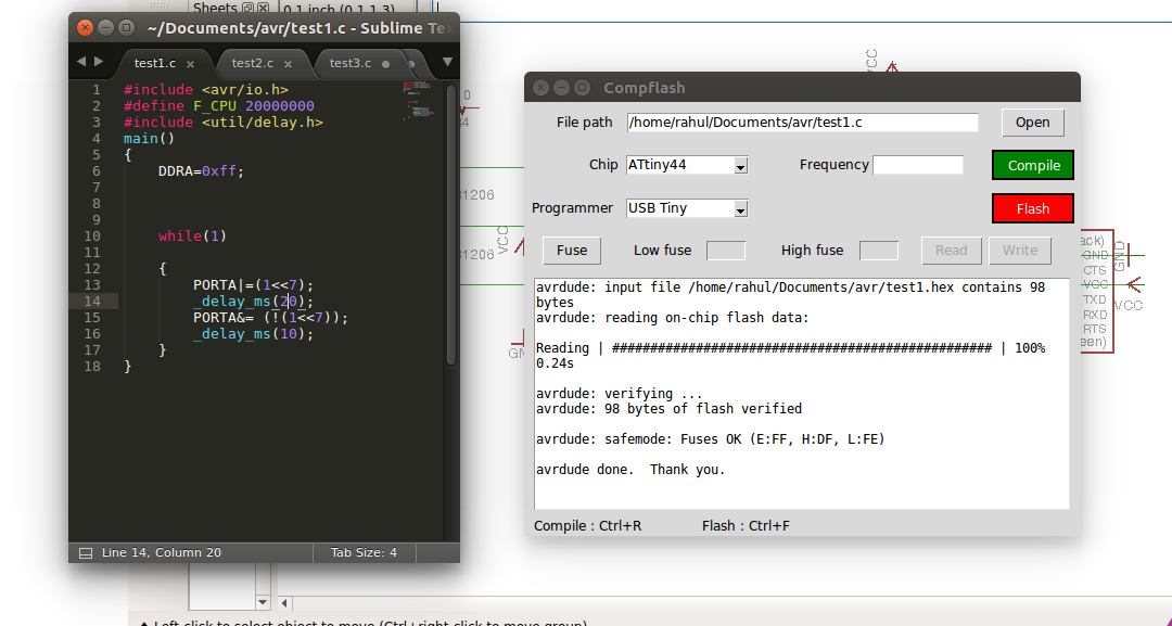
This is a simple program I wrote to blink the LED on my board. The program is written in Atom and flashed onto the chip via Comflash The led is connected to the pin PA7.
The logic behind the program is that I have set the DDRA as output by giving the HEX value oxff. F in HEX is 1111, hence oxff is equal to ob11111111.
ComFlash is a python GUI that one of our instructors wrote to automate the process of compiling and making a hex file from the c program and flashing it with avrdude. It is easy to use and efficient, it really helps when you want to quickly edit some values of the code, compile and flash it on to the chip. All of my C programs are flashed on to the chip using this method.
The way to use it is to open your program from the menu and click Compile to compile the code, it will give the result and show any error if any in the program.Then Select your chip and your programmer from the drop-down menu and click Flash. It will then flash the chip with the code.
You can find it on GITHUB/yadhusharon
This is a simple program to turn on the LED when the button is pressed. T
    #include <avr/io.h>
#define F_CPU 20000000
    #include <util/delay.h>
main()
{
  DDRA=0xff;     // set PA0 to PA7 as output
  DDRB=0x0;     // set PORTB as input
  PORTB|=(1<<PB2); // pullup PB2

	while(1)

	{
    if (!(PINB&(1<<PB2))) //check if button is pressed
		{
    	PORTA|=(1<<7); //Turn on LED
    }
  else
  {
    PORTA&=(0<<7); //Turn OFF lED
  }

}
Interrupts are events that require immediate attention by the microcontroller. When an interrupt event occurs the microcontroller pause its current task and attends to the interrupt by executing an Interrupt Service Routine (ISR) at the end of the ISR the microcontroller returns to the task it had pause and continue its normal operations. In order for the microcontroller to respond to an interrupt event the interrupt feature of the microcontroller must be enabled along with the specific interrupt. This is done by setting the Global Interrupt Enabled bit and the Interrupt Enable bit of the specific interrupt.
An Interrupt Service Routine (ISR) or Interrupt Handler is a piece of code that should be execute when an interrupt is triggered.
Interrupt Flags and Enabled bits
Each interrupt is associated with two (2) bits, an Interrupt Flag Bit and an Interrupt Enabled Bit. These bits are located in the I/O registers associated with the specific interrupt:
The interrupt flag bit is set whenever the interrupt event occurs, whether or not the interrupt is enabled or not.
The interrupt enabled bit is used to enable or disable a specific interrupt. Basically is tells the microcontroller whether or not it should respond to the interrupt if it is triggered.
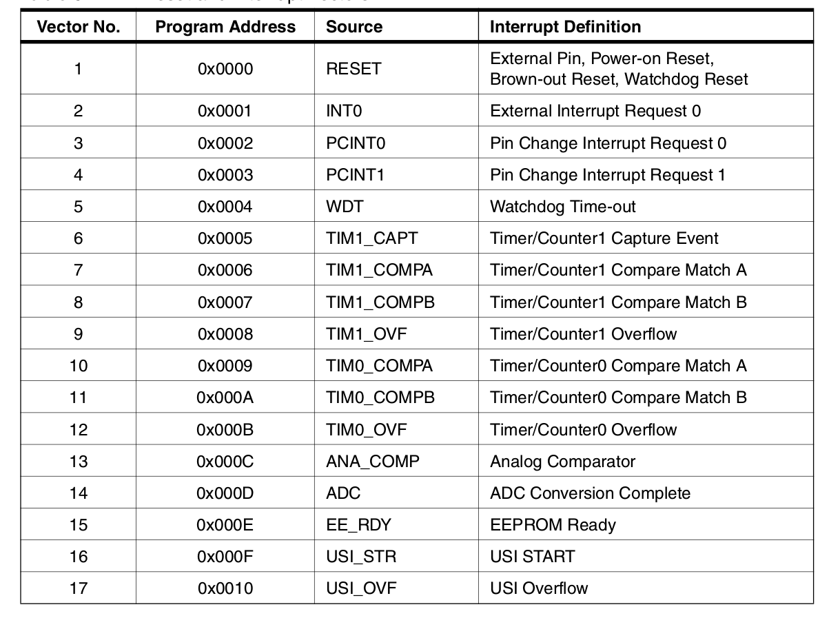
While going through the data-sheet, I identified the registers that need to be set for interrupt programming, the first one is the interrupt vector table for Attiny 24A/44A/84A. I have used PCINT0 Pinchange interrupt vector 0. when a pin change occurs on the Port the ISR will be called.
The INT0 interrupts can be triggered by a falling or rising edge or a low level.A low level interrupt on INT0 is detected asynchronously. This means that the interrupt source can be used for waking the part also from sleep modes other than Idle
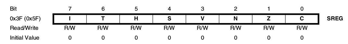
Bit 7 – I: Global Interrupt Enable The Global Interrupt Enable bit must be set for the interrupts to be enabled. The individual inter- rupt enable control is then performed in separate control registers. If the Global Interrupt Enable Register is cleared, none of the interrupts are enabled independent of the individual interrupt enable settings. The I-bit is cleared by hardware after an interrupt has occurred, and is set by the RETI instruction to enable subsequent interrupts. The I-bit can also be set and cleared by the application with the SEI and CLI instruction.,/p> The interrupt execution response for all the enabled AVR interrupts is four clock cycles mini- mum. After four clock cycles the Program Vector address for the actual interrupt handling routine is executed. During this four clock cycle period, the Program Counter is pushed onto the Stack. The vector is normally a jump to the interrupt routine, and this jump takes three clock cycles. If an interrupt occurs during execution of a multi-cycle instruction, this instruction is completed before the interrupt is served. If an interrupt occurs when the MCU is in sleep mode, the interrupt execution response time is increased by four clock cycles. This increase comes in addition to the start-up time from the selected sleep mode. A return from an interrupt handling routine takes four clock cycles. During these four clock cycles, the Program Counter (two bytes) is popped back from the Stack, the Stack Pointer is incremented by two, and the I-bit in SREG is set.
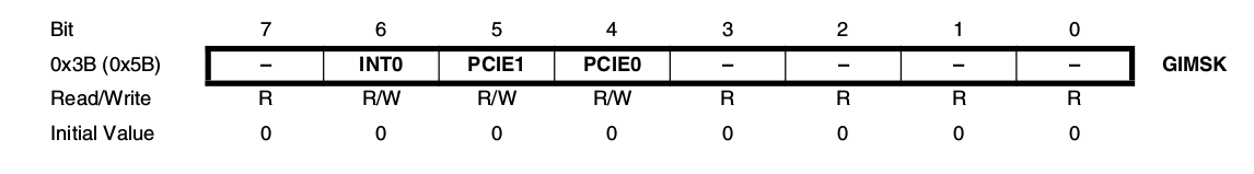
Bit 6 – INT0: External Interrupt Request 0 Enable When the INT0 bit is set (one) and the I-bit in the Status Register (SREG) is set (one), the exter- nal pin interrupt is enabled. The Interrupt Sense Control bits (ISC01 and ISC00) in the External Interrupt Control Register A (EICRA) define whether the external interrupt is activated on rising and/or falling edge of the INT0 pin or level sensed. Activity on the pin will cause an interrupt request even if INT0 is configured as an output. The corresponding interrupt of External Interrupt Request 0 is executed from the INT0 Interrupt Vector. Bit 5 – PCIE1: Pin Change Interrupt Enable 1 When the PCIE1 bit is set (one) and the I-bit in the Status Register (SREG) is set (one), pin change interrupt 1 is enabled. Any change on any enabled PCINT11:8 pin will cause an inter- rupt. The corresponding interrupt of Pin Change Interrupt Request is executed from the PCI1 Interrupt Vector. PCINT11:8 pins are enabled individually by the PCMSK1 Register. Bit 4 – PCIE0: Pin Change Interrupt Enable 0 When the PCIE0 bit is set (one) and the I-bit in the Status Register (SREG) is set (one), pin change interrupt 0 is enabled. Any change on any enabled PCINT7:0 pin will cause an interrupt. The corresponding interrupt of Pin Change Interrupt Request is executed from the PCI0 Inter- rupt Vector. PCINT7:0 pins are enabled individually by the PCMSK0 Register.
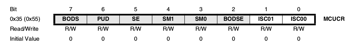
Bits 1:0 – ISC01, ISC00: Interrupt Sense Control 0 Bit 1 and Bit 0 The External Interrupt 0 is activated by the external pin INT0 if the SREG I-flag and the corre- sponding interrupt mask are set. The level and edges on the external INT0 pin that activate the interrupt are defined in Table given. The value on the INT0 pin is sampled before detecting edges. If edge or toggle interrupt is selected, pulses that last longer than one clock period will generate an interrupt. Shorter pulses are not guaranteed to generate an interrupt. If low level interrupt is selected, the low level must be held until the completion of the currently executing instruction to generate an interrupt.

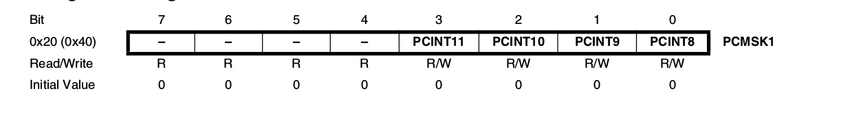
Bits 7:4 – Res: Reserved Bits and will always read as zero. Bits 3:0 – PCINT11:8: Pin Change Enable Mask 11:8 Each PCINT11:8 bit selects whether pin change interrupt is enabled on the corresponding I/O pin. If PCINT11:8 is set and the PCIE1 bit in GIMSK is set, pin change interrupt is enabled on the corresponding I/O pin. If PCINT11:8 is cleared, pin change interrupt on the corresponding I/O pin is disabled.
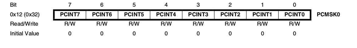
Bits 7:0 – PCINT7:0: Pin Change Enable Mask 7:0 Each PCINT7:0 bit selects whether pin change interrupt is enabled on the corresponding I/O pin. If PCINT7:0 is set and the PCIE0 bit in GIMSK is set, pin change interrupt is enabled on the cor- responding I/O pin. If PCINT7:0 is cleared, pin change interrupt on the corresponding I/O pin is disabled.
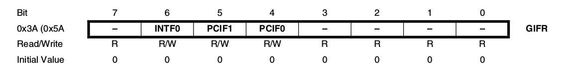
Bits 7, 3:0 – Res: Reserved Bits These bits are reserved in the ATtiny24/44/84 and will always read as zero. Bit 6 – INTF0: External Interrupt Flag 0 When an edge or logic change on the INT0 pin triggers an interrupt request, INTF0 becomes set (one). If the I-bit in SREG and the INT0 bit in GIMSK are set (one), the MCU will jump to the cor- responding Interrupt Vector. The flag is cleared when the interrupt routine is executed. Alternatively, the flag can be cleared by writing a logical one to it. This flag is always cleared when INT0 is configured as a level interrupt. Bit 5 – PCIF1: Pin Change Interrupt Flag 1 When a logic change on any PCINT11:8 pin triggers an interrupt request, PCIF1 becomes set (one). If the I-bit in SREG and the PCIE1 bit in GIMSK are set (one), the MCU will jump to the corresponding Interrupt Vector. The flag is cleared when the interrupt routine is executed. Alter- natively, the flag can be cleared by writing a logical one to it. Bit 4 – PCIF0: Pin Change Interrupt Flag 0 When a logic change on any PCINT7:0 pin triggers an interrupt request, PCIF becomes set (one). If the I-bit in SREG and the PCIE0 bit in GIMSK are set (one), the MCU will jump to the corresponding Interrupt Vector. The flag is cleared when the interrupt routine is executed. Alter- natively, the flag can be cleared by writing a logical one to it.
Here is the C code.
#include#define F_CPU 20000000 #include<util/delay.h> #include<avr/interrupt.h> ISR(INT0_vect) { //interept service routine while interept is made by int0 pin while (1) { if (!(PINB&(1<<PB2))) { // if PB2 is low PORTA|=(1<<PA7); // set PA2 High // set PA2 High } else // else break; // set PA2 Low } } main() { DDRA=0xff; // set PA0 to PA7 as output DDRB=0x0; // set PORTB as input PORTB|=(1<<PB2); // pullup PB2 MCUCR = 1<<ISC00 ; // Any logical change on INT0 generates an interrupt request. GIMSK|= (1<<INT0); // external pin interrupt is enabled om INT0 pin sei(); // set global interrupt flag while (1) { PORTA|=(1<<7); _delay_ms(500); PORTA&= (!(1<<7)); _delay_ms(500); } }
I used the interrupt function to jump from the main program to interrupt program when the button is pressed. The main program is a blinking LED program set to blink the LED, every 500ms and the Interrupt is to turn ON the led continuously.
Arduino is an open-source platform used for building electronics projects. Arduino consists of both a physical programmable circuit board (often referred to as a microcontroller) and a piece of software, or IDE (Integrated Development Environment) that runs on your computer, used to write and upload computer code to the physical board. There are a large collection of tutorials are available on Arduino, out of which ,I found the following tutorial is good to know more about Arduino.
Ardunio is basically AVR C with an extra layer on top of it. For beginners like me Arduino is relatively easier to learn than AVR C. This is because in the Arudino IDE most of the common tasks we have to do are written as functions and stored in the Arduino library. This makes it easier for beginners as all we have to is call the right functions and the program will work accordingly. But a downside of this is that, the chip will work much slower than if it was programmed with AVR C the reason is that Arduino loads a lot of unused libraries into the chip which will waste many clock cycles. Another problem is the size of the program itself, this will be much larger in comparison with AVR C program.
After Installing Arduino in Linux, I plan to program my board using Fab ISP through arduino IDE. Arduino IDE supports all default Arduino boards, but in order to work with external boards, we have to first add the boards through the board manager.
You can follow this tutorial to add the Attiny44 board to the Arduino IDE.
Here are the steps,
https://raw.githubusercontent.com/damellis/attiny/ide-1.6.x-boards-manager/package_damellis_attiny_index.json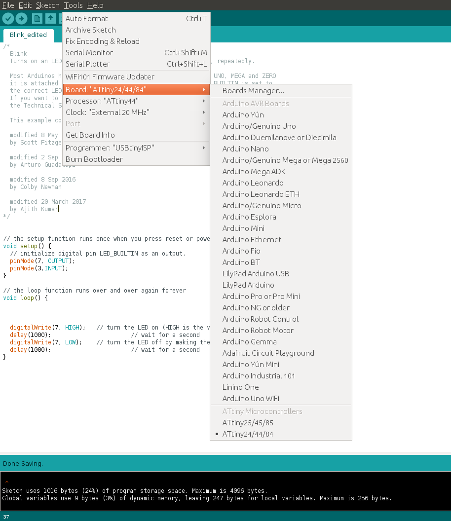
Now you have successfully added the board, you can begin programming.
Arduino has some example programs to get you started. I went through the LED blink program and edited the source code. I changed the pins of the program to correspond to the pins on my board after referring the Arduino pin out diagram of ATtiny. The program was flashed successfully after burning the Arduino bootloader.
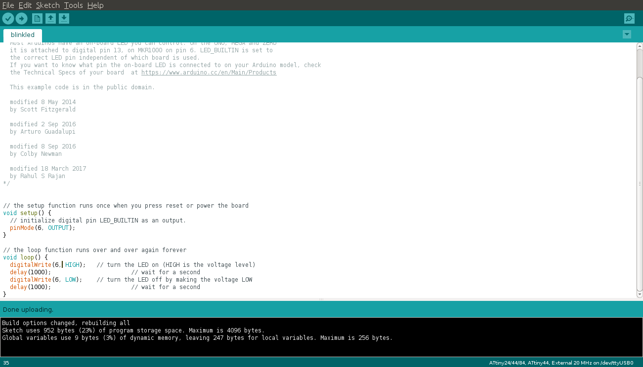
The program size was 952 bytes, When compared to the same program written in AVR C (457 bytes), is almost double. This is the extra overhead I talked about when using Arduino. Its useful for prototyping quick projects but not suitable for running finished products.
I learned a lot about programming Micro controllers this week, but I know there is still more I need to learn about. I'm familiar with C++, but still need more practice with C. In the future I want to learn more about using the in built hardware of the MCU, like timers, registers, ADC etc. This would be the next step, as I want to leverage the full capabilities of these Micro controllers.
rahulsrajan.com
rahulsrajan01@gmail.com
Trivandrum, Kerala ,
India.

Technopark, Kerala, India