Week 6 - PCB designing
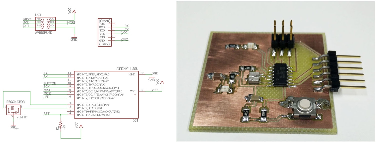
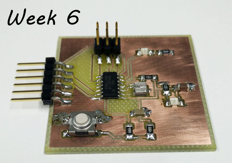
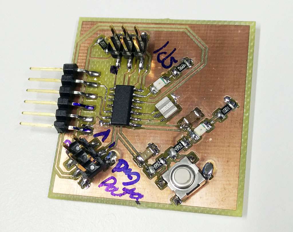
This week was circuit board designing week. To start with we had a ready made board with ATtiny44-prosessor and some supplementary components. To get familiar with the process we needed to add at least a led and a button to the design and make the board. Due to my winter holiday, I swiftly made a board with these specifications. But later on, I found out, I had some extra time so I made a little more complicated one, with power on -led and couple extra IO-pins to the connector.
To start I need to install the pcb design tool. I desided to use Eagle so first thing was to install Eagle software. Download Eagle from Autodesk www-page and install to directory suitable for you. Suggested place is C:/.
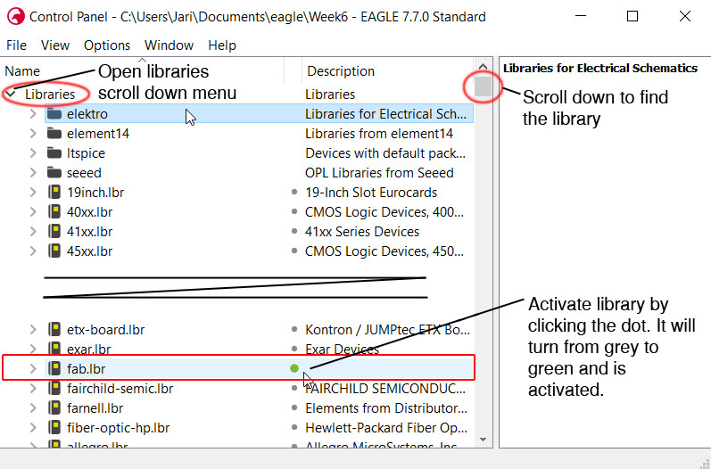
Next download the fab.lbr and activate it. Fab library hold most of the Fab Lab inventory componets.
To be able to make a pcb with Eagle, you need the component descriptions of components you are about to use. In Eagle the components come in sets that are called library. Eagle come with lot of different components already, but usually you still need some others that are not in library. You can design them on your own i.e. create you own library and components in it. For this course Fab Academy has made a library of components that are available at FabLab. To get these components you need to download the .lbr file and put it in right Eagle folder for the software to find it. At my computer Eagle library folder is in C:/Eagle-7.7.0/lbr where I added the downloaded library file fab.lbr.
Now that you have you library file in right location you need to activate it in Eagle. This is done in Eagle main screen. On the left side of the panel, click the Libraries. This will open a tree showing all available libraries. Scroll down until you find the fab.lbr and click the small grey dot on the right side of the library name, it will turn to green and the library is activated. On the picture, only the fab.lbr is active, all others have grey dot next to them meaning they are not activated and when you add components later in eagle, you will not see these component libraries and their components there.
Drawing the schematic
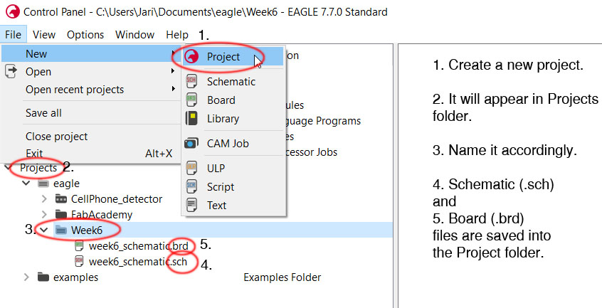
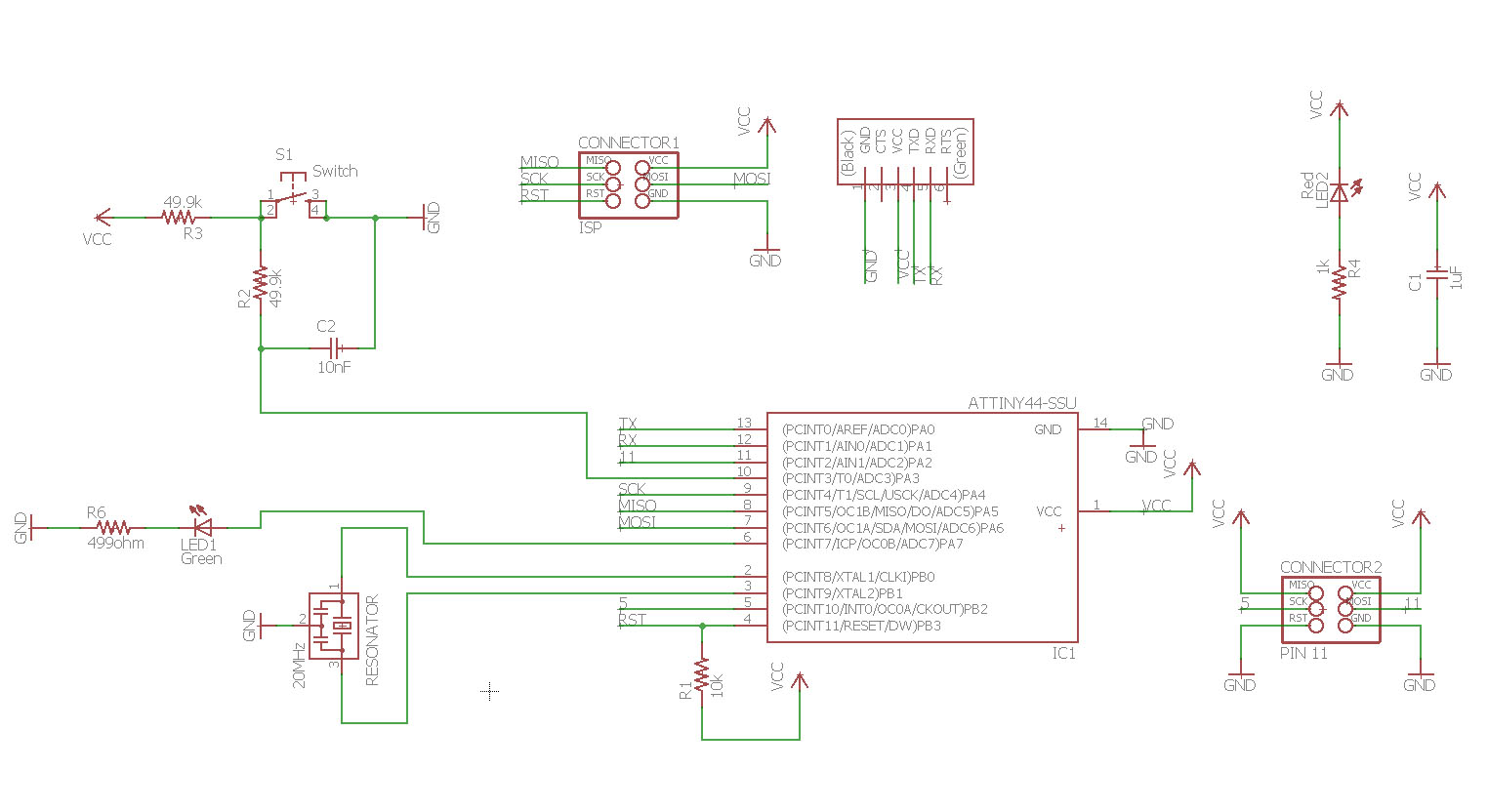
When designing the board, first we have to add the components to the schematic and connect them in right way. When starting new design go to eagle File -> New -> Project or you can start by creating a new Schematic. If you create a new project, then create a new schematic. It will be saved in th new project file. Later on when board file is created that will be in the same folder as well.
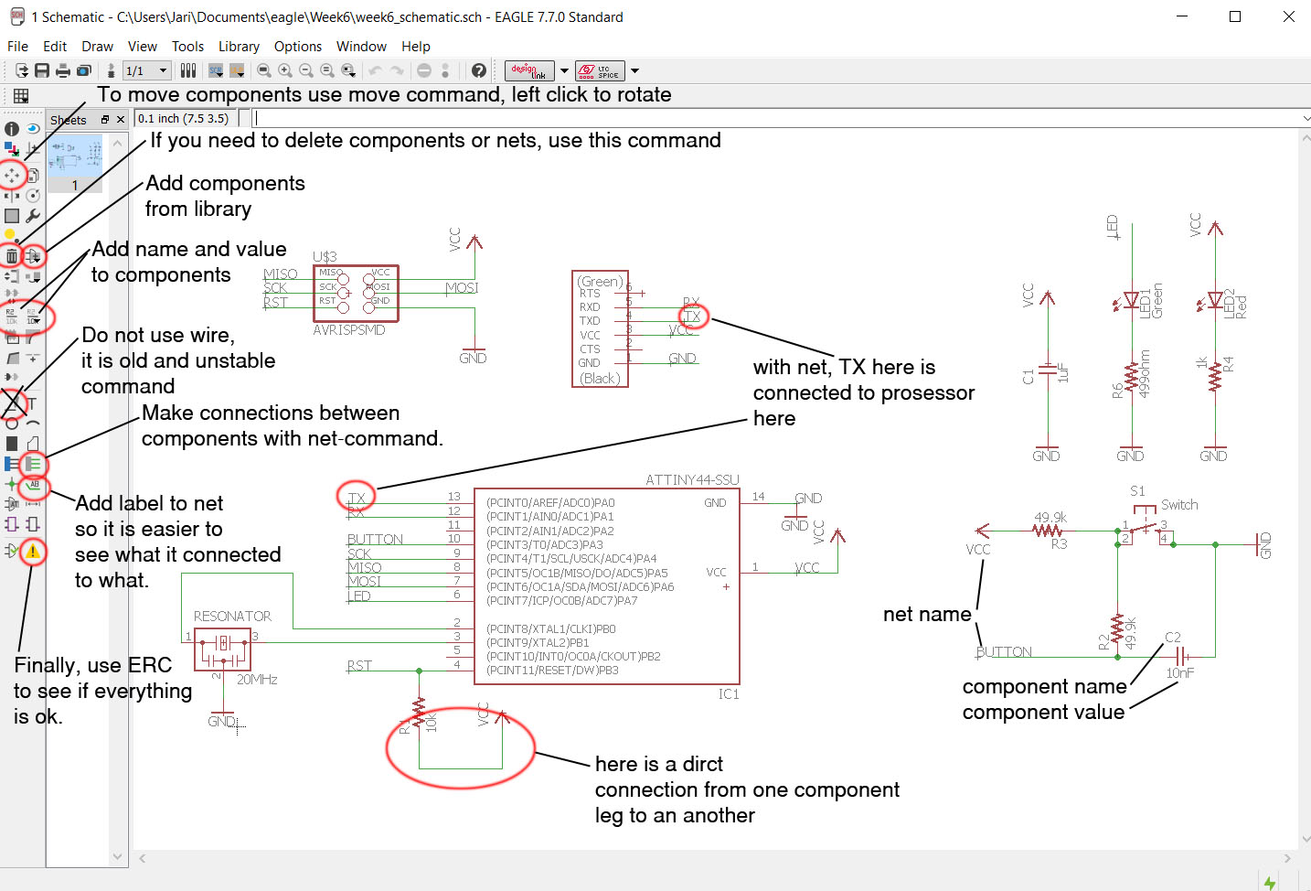
Now we are ready to draw the schematic. Add the components you are using by using add command. Use Net command to connect everything as they should be connected. You can use multible ground and positive power i.e. VCC points to make the schematic more clear. You can eather make direct connection from component to component by net or by naming the wire with same name, and they will be connected. Move components with move commmand and rotate them by left clicking when move command is selected. It is good to give name and value to components. When you name a net, you can connect other parts to it by naming them with same name. Value is at this point to clarify design visually. If simulation would be used, then values would be critical. Labeling the the nets will make reading the schematic more clear. DO NOT USE wire-command! It is old and unstable, always use net-command to connect legs of components.
Run Electric Rule Check (ERC) at the and to see if everything is connected.
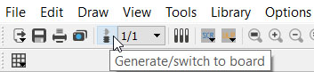
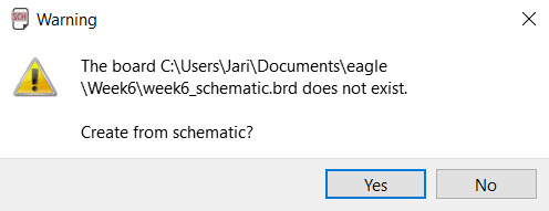
Next click the Generate/switch to Board button to start the board generation. Or later on you can go from schematic to board and back again while designing the board. Eagle will ask you if you want to generate the board from this schematic when doing this the first time. Just say yes and you will be taken to the board design window.
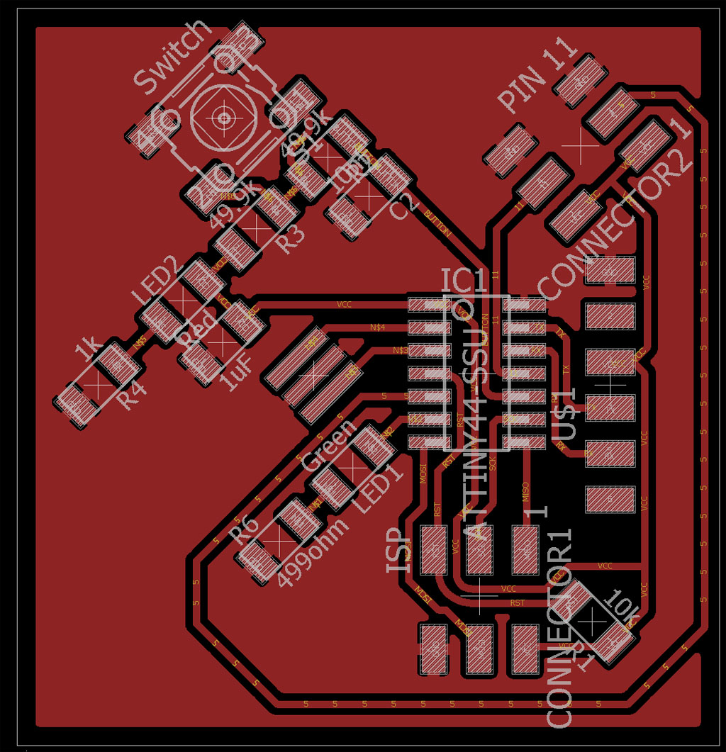
Drawing the board
All the components visualised on board designer as their footprint i.e. what kind of legs they have and what type of pad they need. And they will be connected by thin wire to show what leg should be connected to what on the board with actual wire. On free Eagle you can use only "positive quarter" of the design area, so you need to put all the components to right and up from origo point. If you are using paid version, this restriction is not valid.
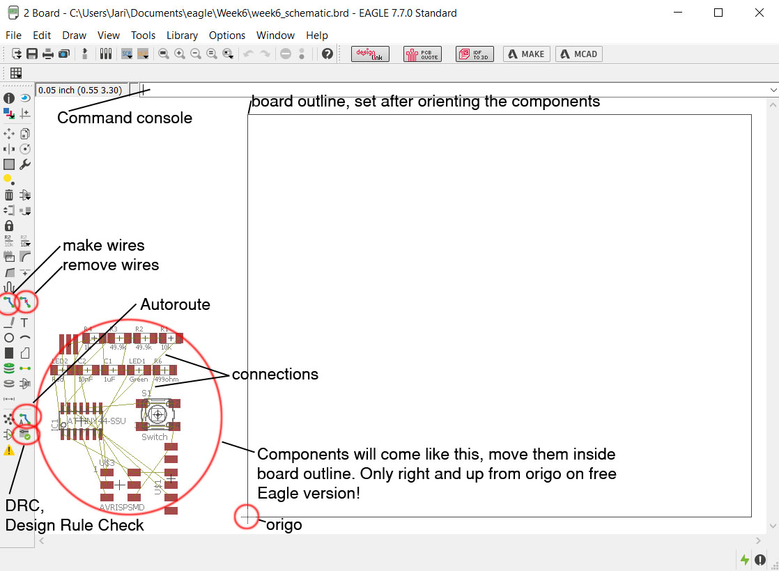
Move the components around and draw the wires, or use Autoroute after placing the components. After Autoroute there might be wire not connected. If this is the case, or you see that some component would be better located somewhere else, use Route and Ripup -commands (on the picture they are named Add wires/remove wires). You can route everything manually, try to make it with Autoroute command or as I did, I use both in combination. First I place the components, then I Autoroute, then I see if some components are better off somewhere else, move them and then Autoroute again. I keep doing this as long as needed. To remove wires Autoroute does or are done by hand, use the Ripup commmand. If all the wires have to be removed use commmand: ripup ; at the command console, this will remove all wires.
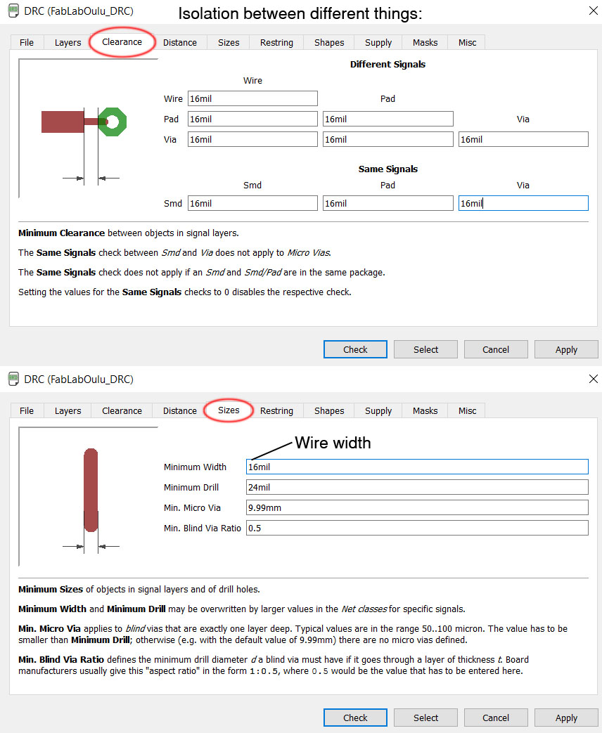
After finishing the board design, use Design Rule Check (DRC) to make sure that the isolations are ok. If you have not set the DRC-rules, you must do it after opening the DRC window.
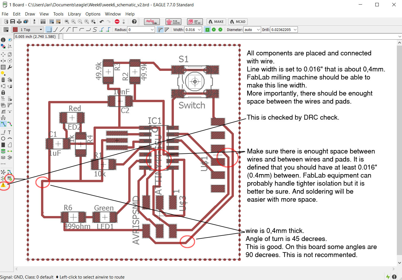
Now that the board is ready, make the Design Rule Check (DRC). I used 16 mils isolation as rule. DRC-file is shared at the end of the page.
When board passes DRC, it is time to make the image file for milling the pcb.
Exporting image-files
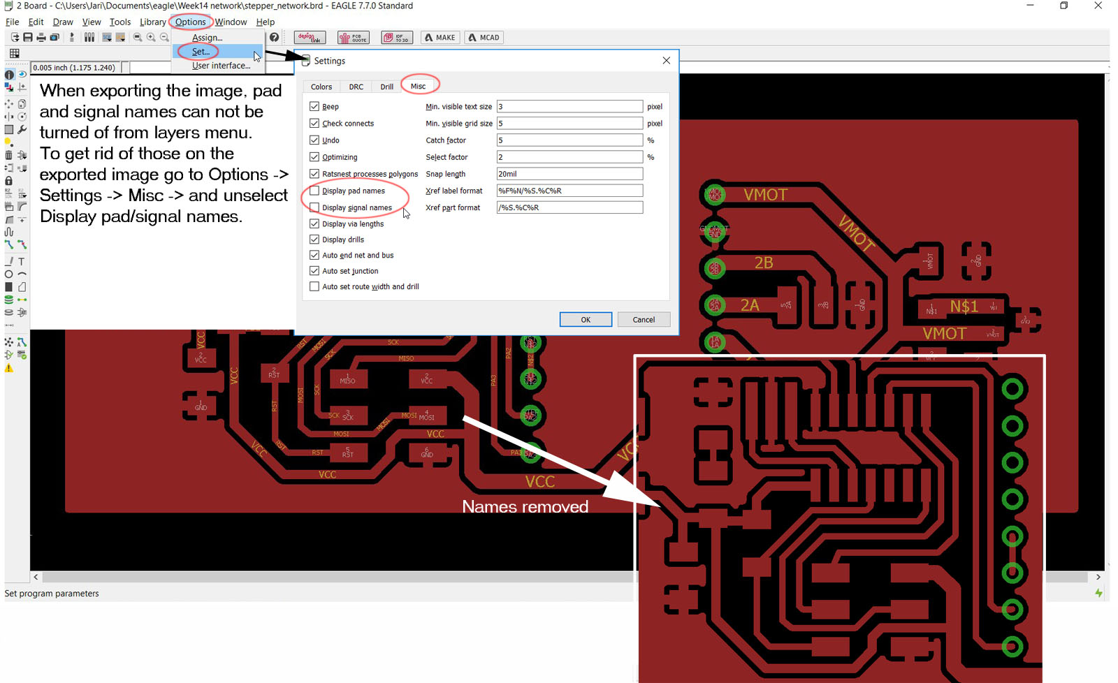
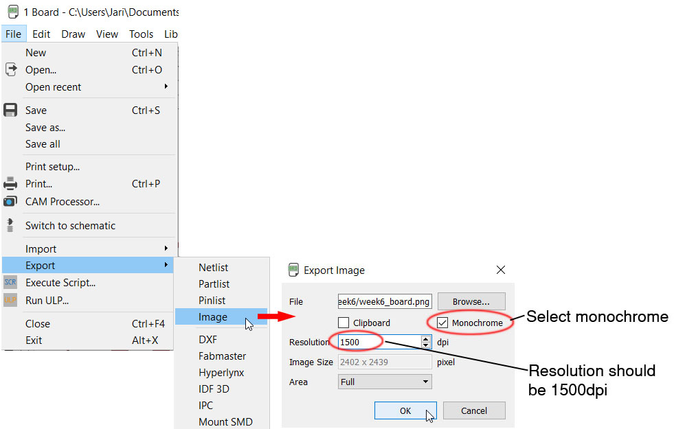
Before going into exporting image file, pad and signal names can be turned off from Options -> Settings (set) -> Misc. untab the "Display pad names" and "Display signal names". This will clear the names from export image.
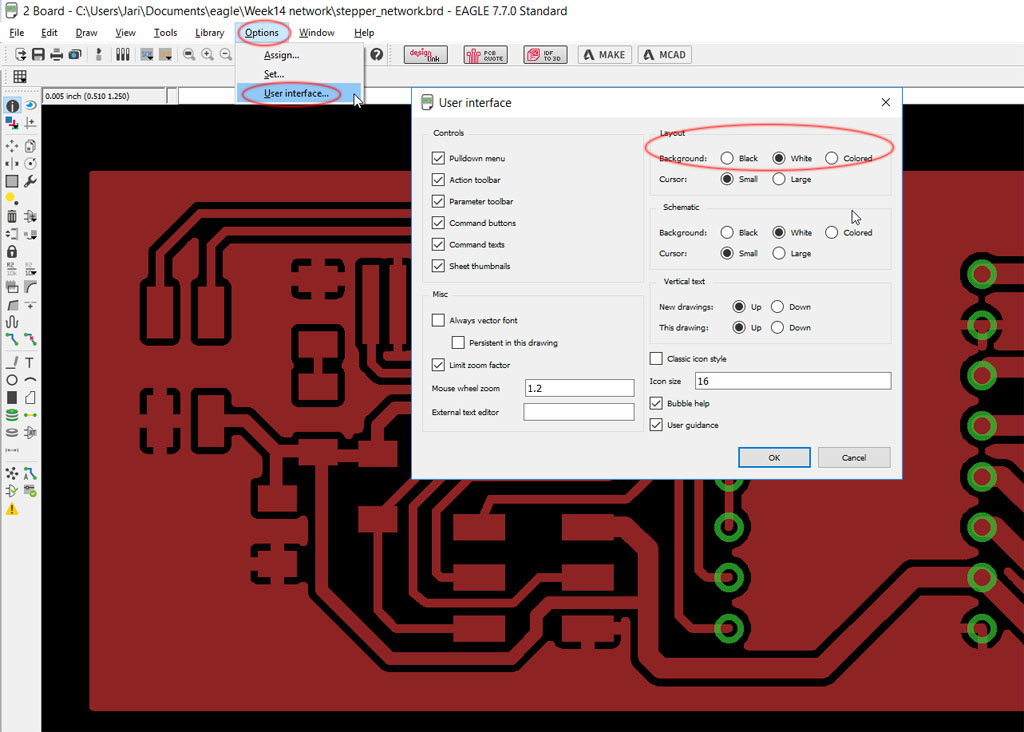
Also if you do not want to reverse colors later on in image prosessing software it can be done in Eagle. From Options -> User Interface select background color as white. Now wires and ground is automatically black and backgound white.
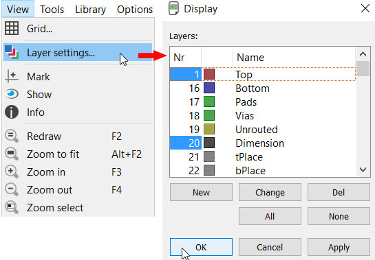
Then we have to make sure not extra data is on the picture that we are about to export. Go to View -> Layer Settings menu and select only top layer (nr. 1). To start with, all layers are active. Press the None-button and then select the ones you want. Then click OK. Go to File -> Export -> Image and select the place where to save the file. Use image settings 1500 dpi and monochrome. Click ok.
Creating images for fabmodules
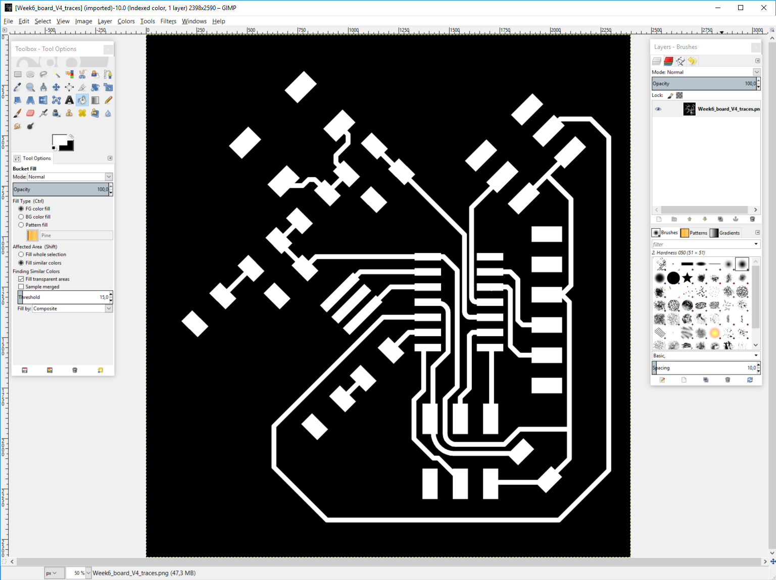
To be able to mill the boards using Fabmodules, we have to edit the exported .png images. I used the instructions given by the local instructors. With these the traces and cutout .png images are prepared using Gimp software. On this example I have used the second board I designed this week. So it will look different than on other example images used on this page.
- Open the image in Gimp.
- Create a new layer with foreground color as black.
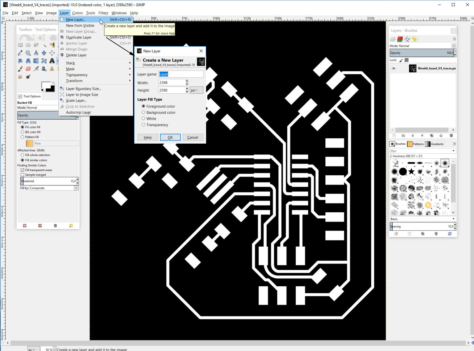
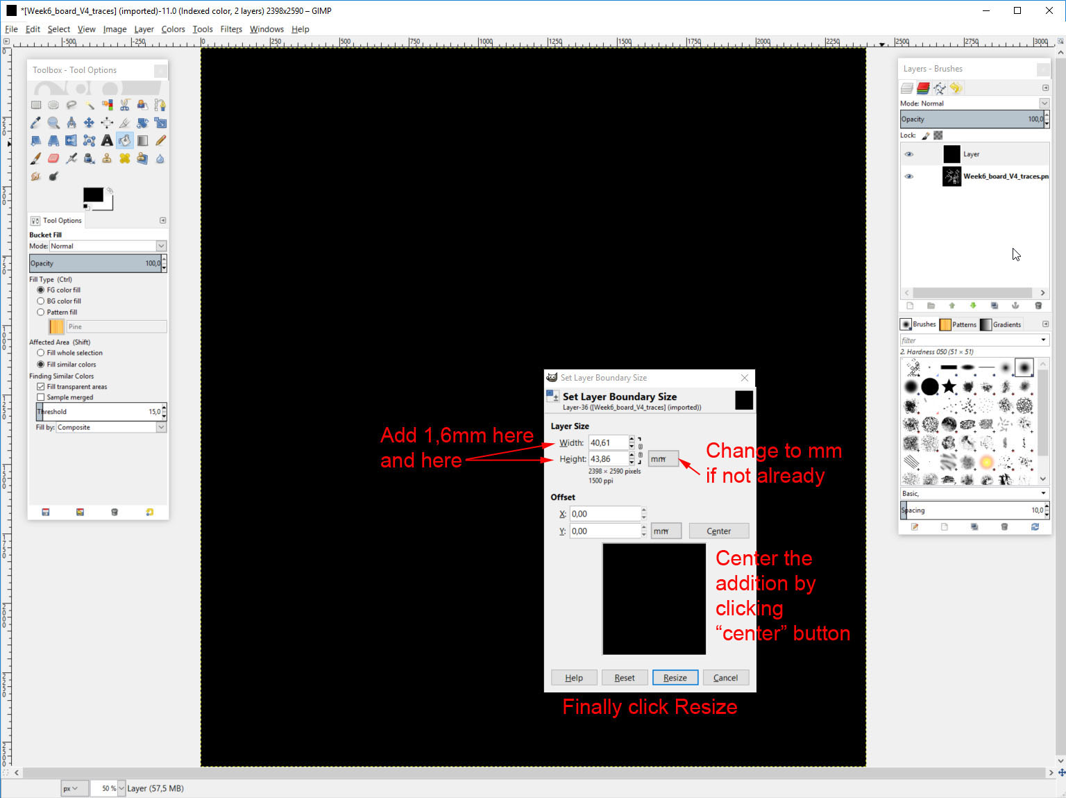
- Set Layer Boundary Size for the outline layer by adding 1.6 mm to width and height centered. This is the margin milled away by the machine with the 0.8mm or 1/32 inch milling bit.
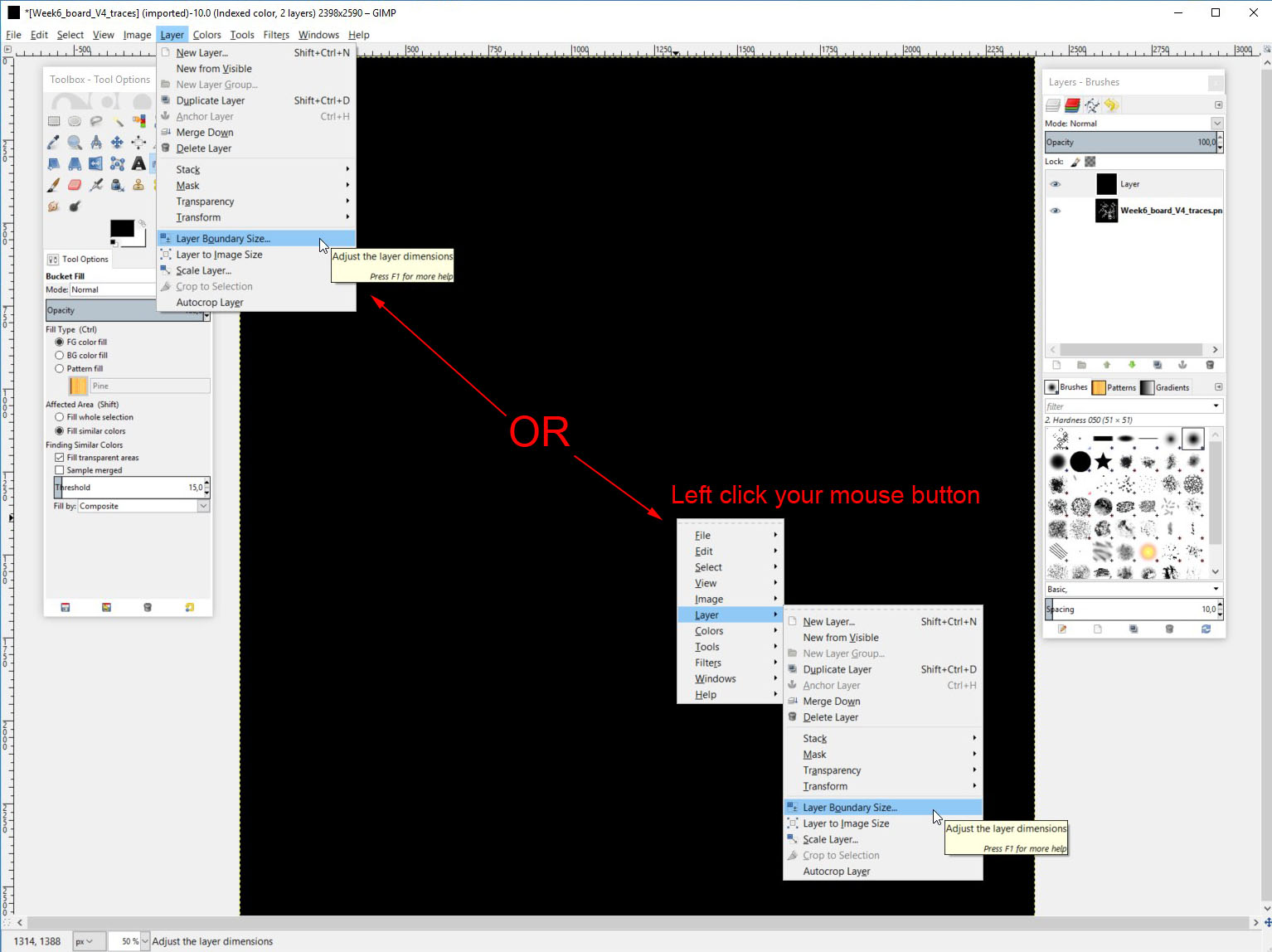
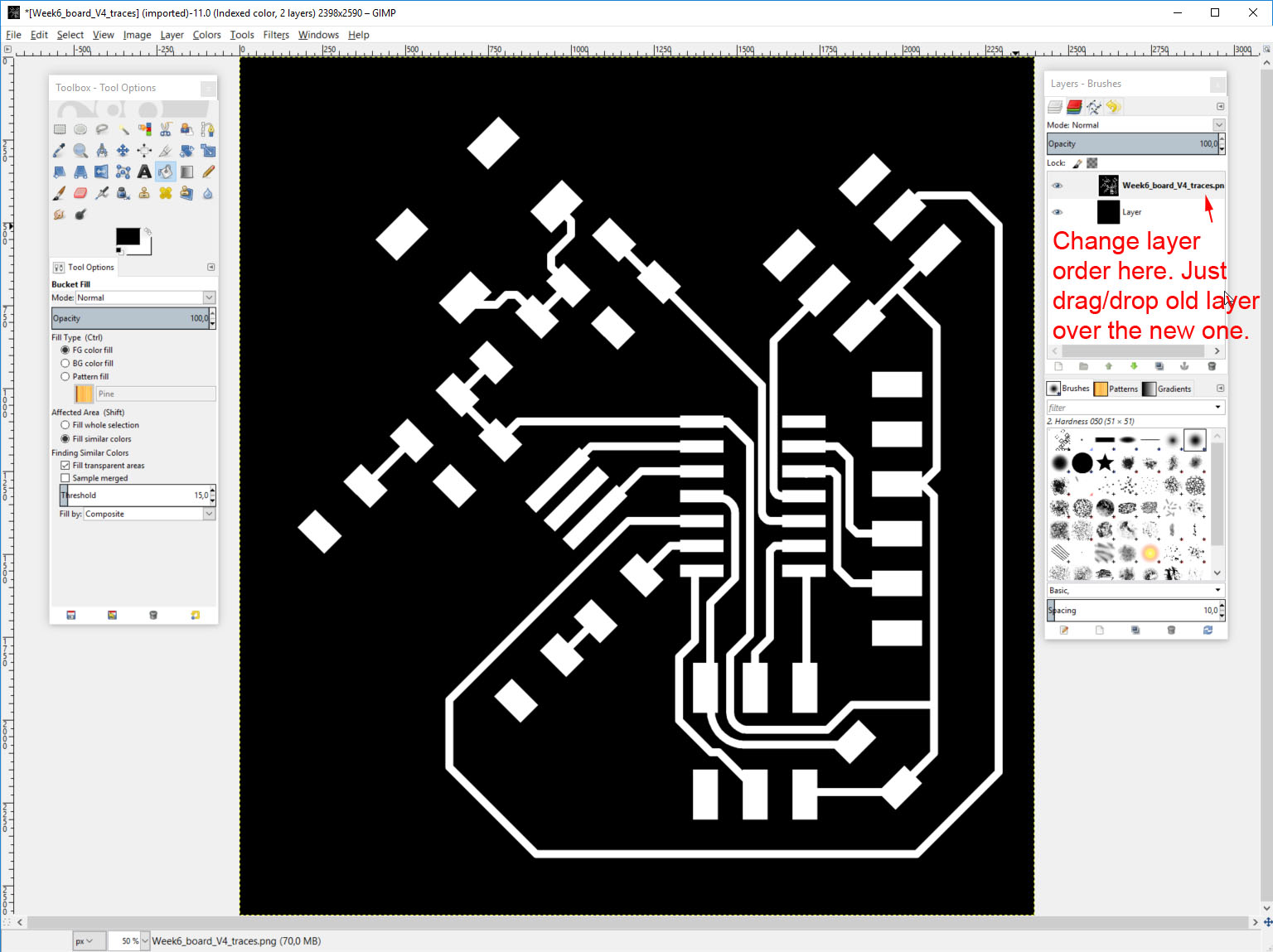
- Change the order of the layers in the Layers tab: on top the traces layer, and below the outline layer.
- Enlarge the image to fit all layers: Image - Fit canvas to layers. Then fill the empty area with black.
- To create the traces image file, export the image as .png.
- To create the cutout image file, fill the traces layer with white and export the obtained image as .png.
- These two files will be used in Fab modules (fabmodules.org) to create the .rml files used by the milling machine.
Let's go through this so it will be clear how it is done. Many of the examples seem to skip some details that are not clear.
First import the image you just created from Eagle. This is done in Gimp by first importing the image. I just used drag/drop method.
Then we need to make a new layer. This is done from layer -> New layer. In new layer properties window select "Layer Fill Type" as Foreground color or any layar that you have as black. The layer color must be black.
This will give us a new black layer on top of the earlier layer. Image will look like this.
Now we need to add some black "material" to the sides of the traces image. We need to do this so that we can create the cutout file. The cutout need 0.8mm or more depending the milling bit around the traces area. This is done by adding 1,6mm to the width and height of this layer. To add the dimensions, left click the image and select layer -> layer boundary size. You can also get here from layer menu.
Then add 1,6mm to both width and height. Then click the "Center" button so the addition will be evenly distributed around the original image.
Now change the order of layers as the traces layer is behind the all black new layer. Do this in layers window.
Finally enlarge the image to fit all layers as the newly done layer is bigger than the original one. And we want them to be same size. Go to Image -> Fit canvas to layers.
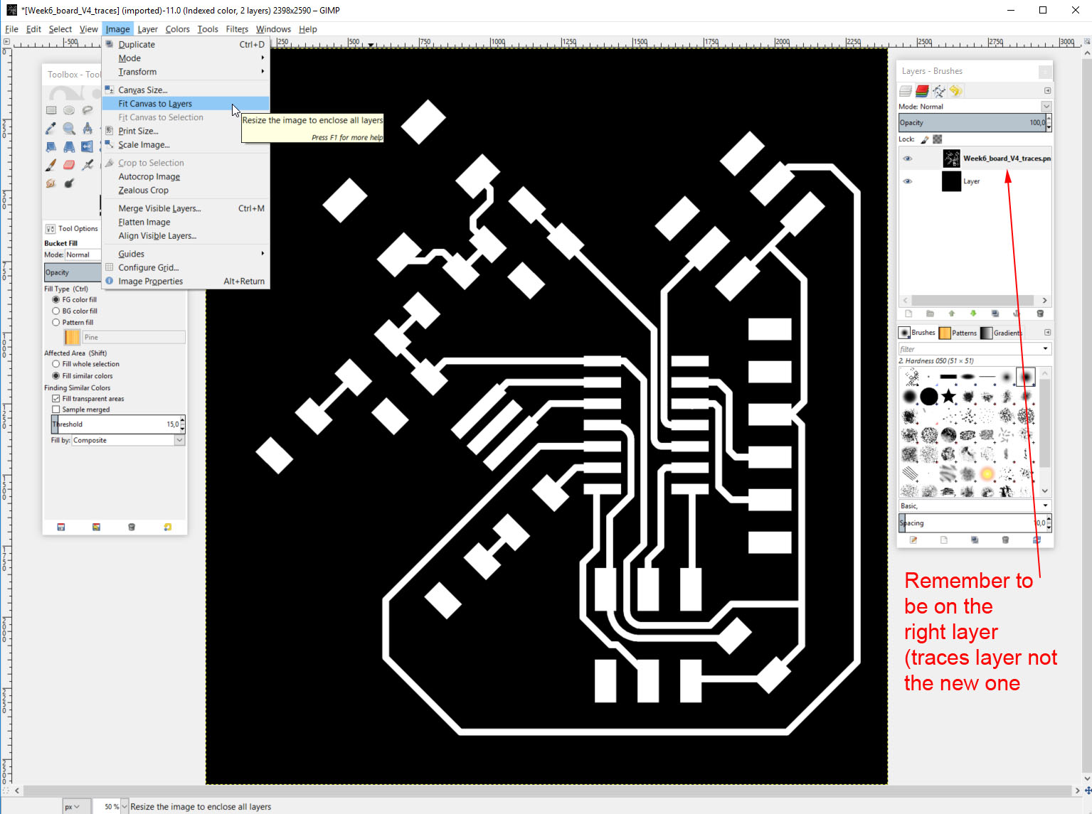
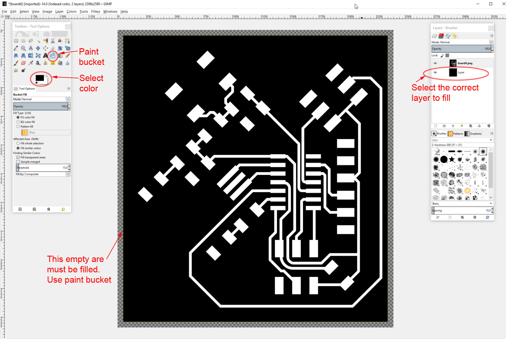
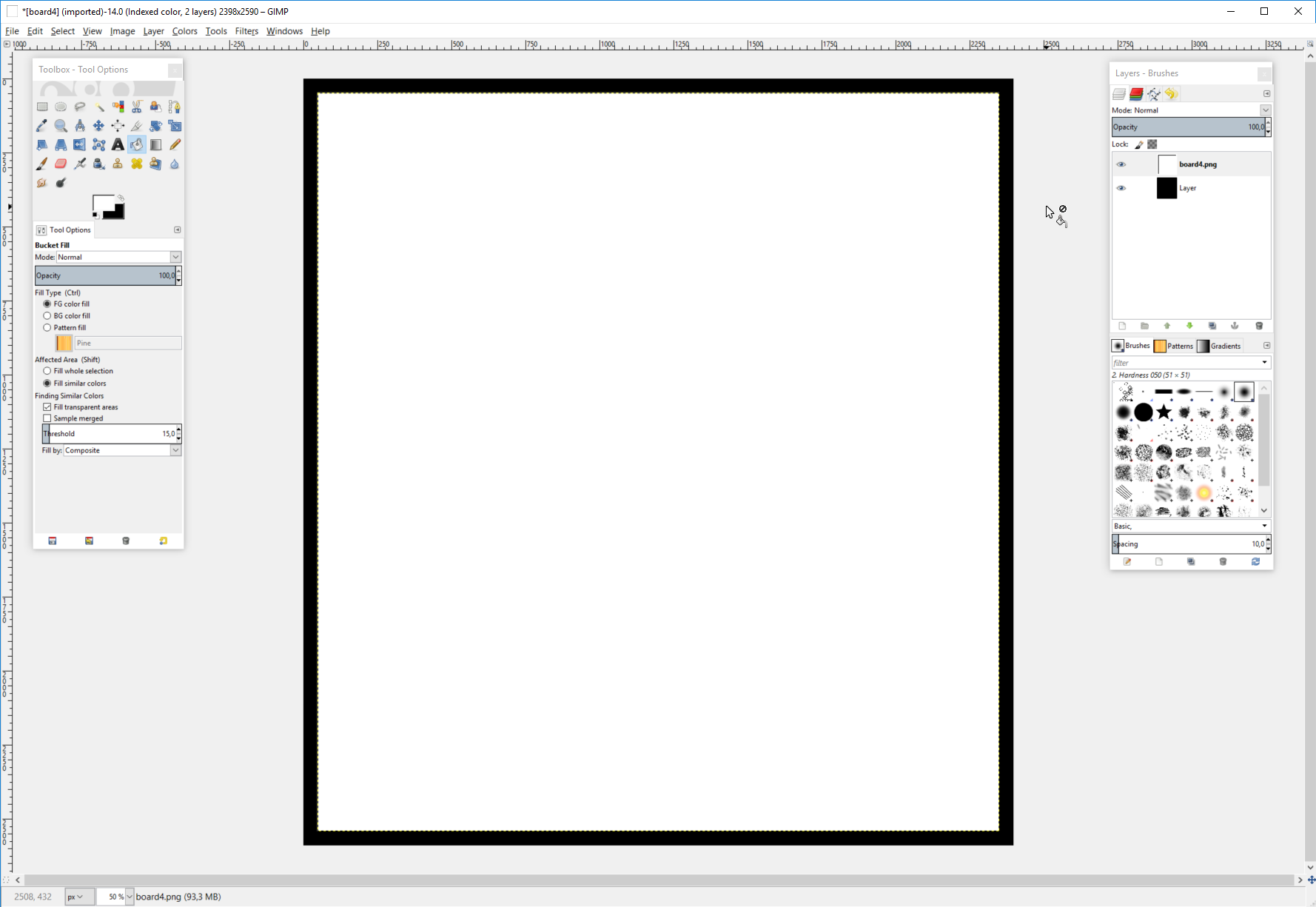
Finally the newly resized layer has some empty area that is the new area. We need to fill it with black. So make sure you are still at the same layer you resized and select paint bucket (or bucket fill tool as it is called in Gimp), color black and fill the empty space with color.
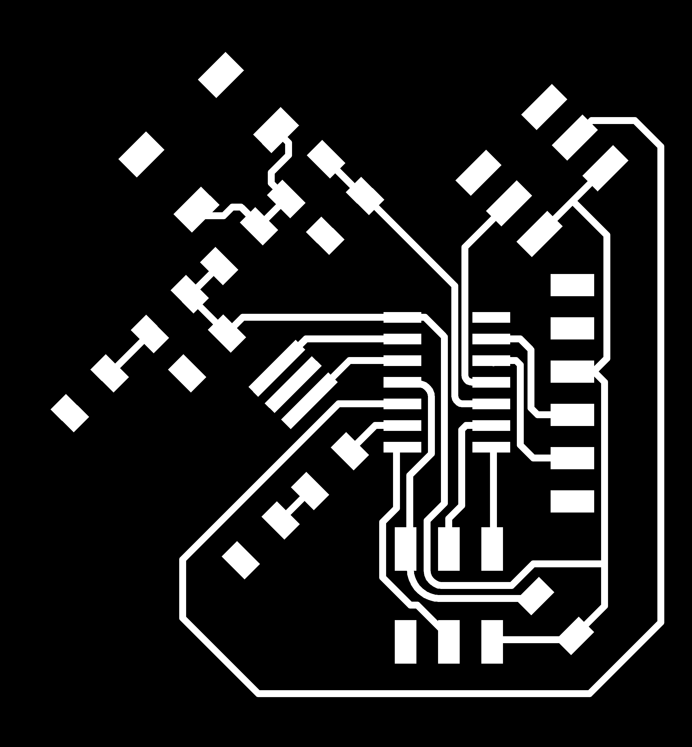
Now we have two layers. One has traces and other the outline. We need to export them as .pgn files. It is good to name them with traces and outline in the name to we recognize them later when milling the files.
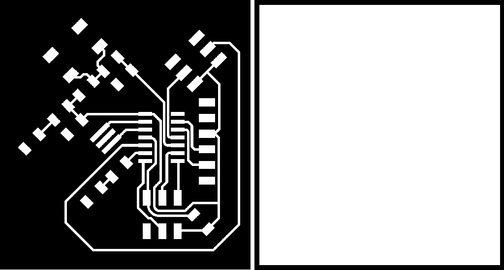
When you have two layers top of each other, traces will be visible as it is on top. Now we can export the traces .png image. To to File -> export and export file with suitable name.
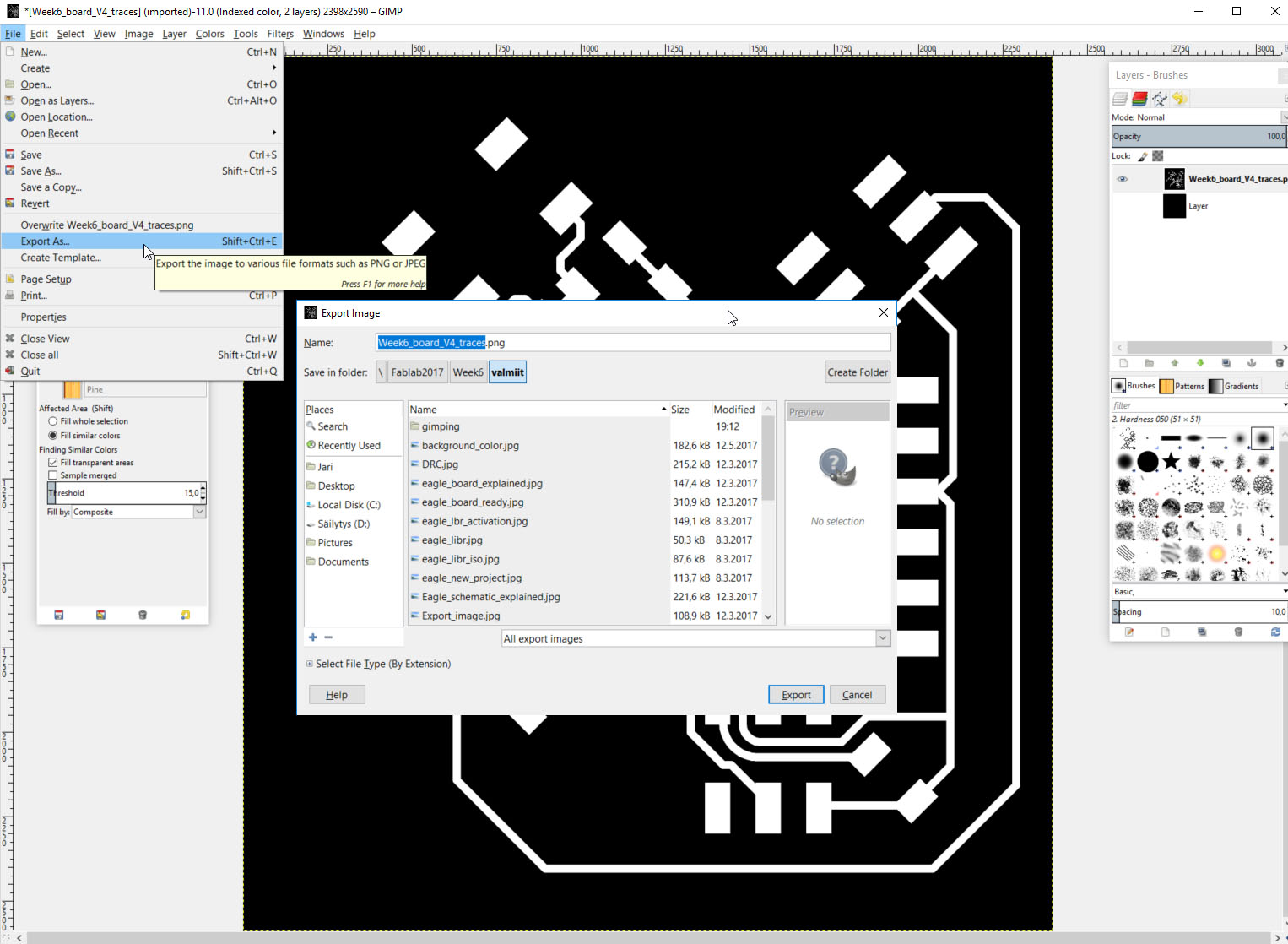
To export the outline. you must select the traces layer and fill it with white color. Filling is explained above. Here is the outline image.
Here is what we get.
Now we have the image to mill the board. This is done like in week 4. Follow the istructions as is explained there. Week 4
Here is the board I made first. The connector on the side should be a little bit too out, so too close to edge of the board.
Board with extra I/O-pins
Here is the other board I made this week just to get experience with Eagle pcb software.
Files used with this weeks assignment
Here are Eagle .sch and .brd files and gerber-files I generated. Also the DRC file used with design rule checks and .job file to make gerbers.
Schematic file for Eagle
Board file for Eagle
DRC file for Eagle
.JOB/.CAM file for Eagle
Top layer gerber file for manufacturing
Outline layer gerber file for manufacturing
Second board .brd file for eagle
Second board .sch file for eagle
Traces .png file for milling machine
Outline .png file for milling machine