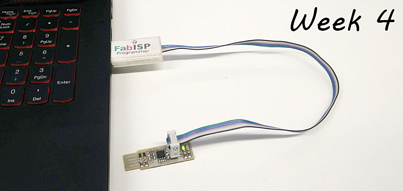
Week 4 - Making an in-circuit programmer
Tasks:
1. Mill in-circuit programmer PCB (printed circuit board)
2. Source the components from FabLab collection
3. Solder components to the PCB
4. Download and set up the programming environment for programming the new programmer.
5. Program the new programmer with some old programmer i.e. other FabISP or some commercial version like Dragon or Atmel-ICE
6. Test new programmer by using it to program something else.
Milling the PCB
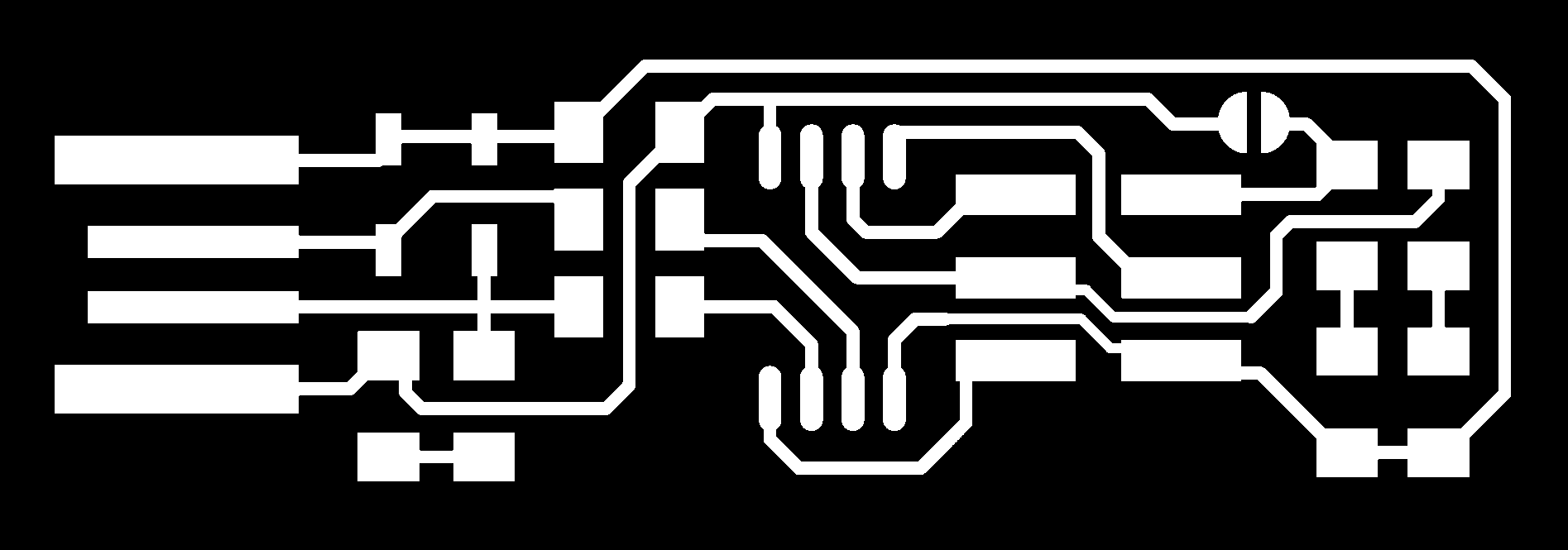
Fab community offered multiple designs from where to choose. I started with one made by Brian called FabTinyISP.
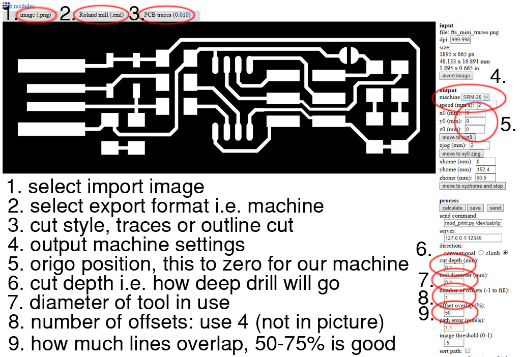
First I downloaded the files i.e. design that was available That included the traces and outline-files. Then I generated the milling files from .PNG pictures using Fab Modules. Software written by Neil. In Fab Modules, milling machine spesific settings must be selected. At our lab I used these setting: Number 6 must be deep enought to remove all copper but there is no point going too deep. Number 8 defines how much copper is removed next to a wire. If it is set to 1 the mill bit will do only one pass, if the setting is for example 4, the bit will run four paraller rounds and here the setting 9 comes in use. Setting number 9 defines how much these paraller runs go on top of each other. If you use a V-shaped drill as we do, Some good overlap like 50-75% in good, so that all the copper is removed. After defining all the settings press the "calculate"-button. After calculation, press the "save"-button to save generated milling file.
And for the outline: Image import and milling machine settings are as earlier. Number 3 defines how deep the mill bit will go at one run. This with the material thickness defines, how many rounds the milling bit has to do to go through the material. You can see each consecutive run at the picture (three in this case).
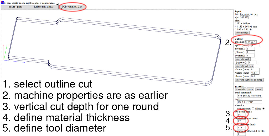
After setting the parameters press the "calculate"-button. And finally "save"-button. Files will be .rlm format. Now that we have files ready. It is time to set up the milling machine.
Setting up the milling machine for PCB manufacturing includes next phases:
1. Set up the blank pcb to the milling machine
2. define origo and drill bit depth
3. import the milling files (.rlm from fabmodules)
4. Milling and removing the ready made pcb
The biggest issue is to set the blank pcb to the milling machine so that it is even. First attach the pcb blank to the bottom support with 2-sided tape. Make sure that there isn't any air or small particles between. Then attach the bottom support to the milling machine bottom plate, if it is not attached already. Use 2-sided tape there as well.
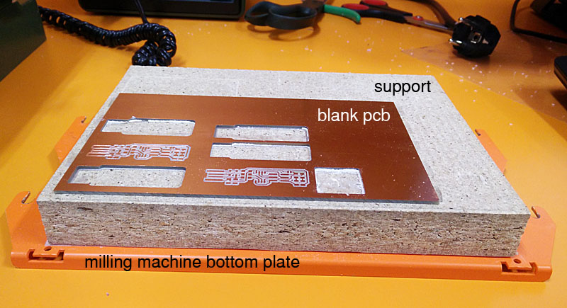
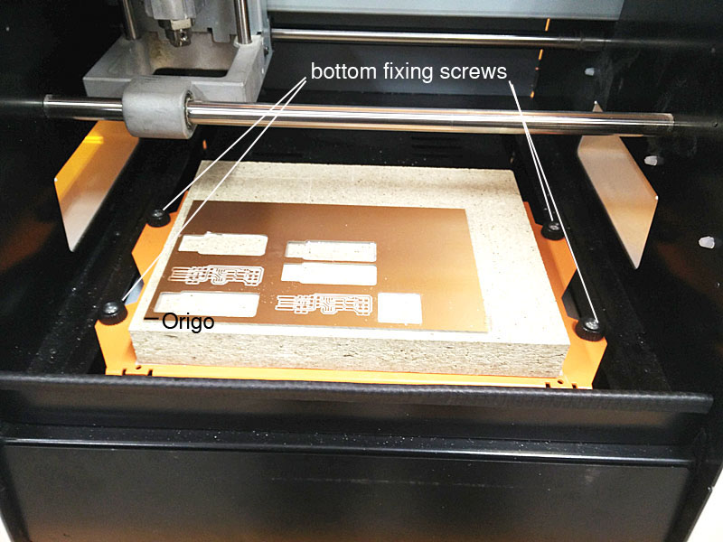
Next attach the whole package to the milling machine. There are 4 screws. Slide the bottom plane in place, press firmly towards back of the machine and tighten the screws. Now the machine is almost ready.
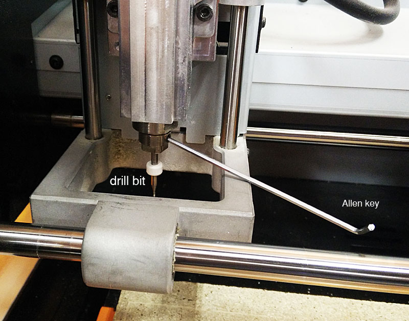
Next the correct milling bit must be but to the machine. This happens by removing the wrong one using allen key. One must take care not to drop the bit. It will break quite easily. Dont push the drill all the way in to the spindle so you have some free movement later when defining the milling depth.
After adding the right milling bit open Vpanel for SRM-20 that is the milling machine user interface software.
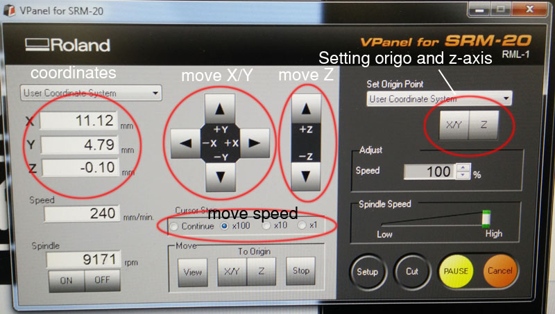
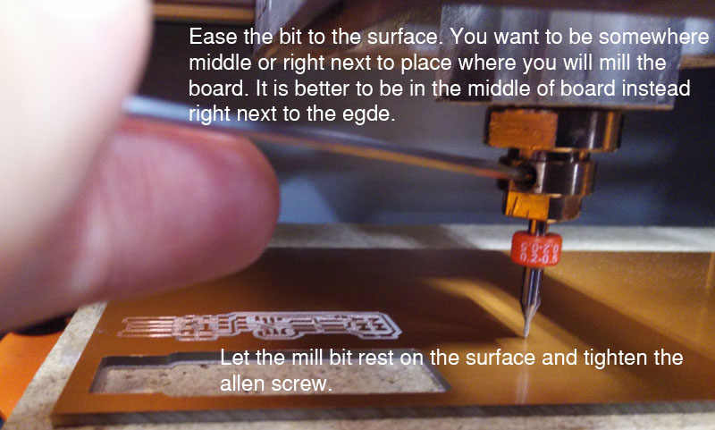
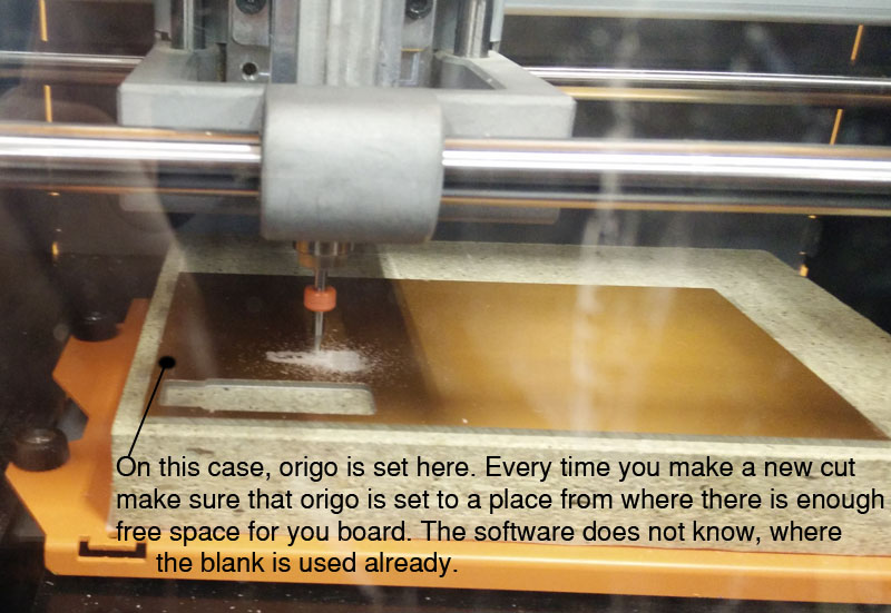
From move X/Y buttons at the middle of the screen move the drilling head to the origo i.e. left front corner of blank pcb. When happy with origo, press the Set Origin Point X/Y button on the right. This will set the origo. It is easier to set the origo when you move the milling bit closer to the surface. Take care not to hit it thought. Next move the z-axes, using z-button up/down, down close to pcb surface. Be carefull not to hit the sufrace. Use "cursor step" (move speed in picture there) options to control your movement. Stop the mill bit head close to the surface. Use Allen key to loosen the mill bit and ease it to the surface. This will be the depth setting. Tighten the Allen screw again and accept the new depth by pressing the Set origin Point Z-button at right top of the VPanel. This will set the new z-axis zero point. You can see the zero set on the left top side on the VPanel (Coordinates).
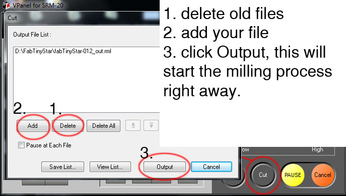
This will finnish the milling machine setup. Time to load the milling files and run them. This happens in VPanel. Push the Cut-button and an file selection window opens. Clear all old milling files by pushing the Delete/Delete all -button. Then use Add-button and find the file you want to mill. Pressing Output-button will start the selected milling so make sure that everything else is set and you have the right file selected.
Finally milling machine is doing it job and milling.
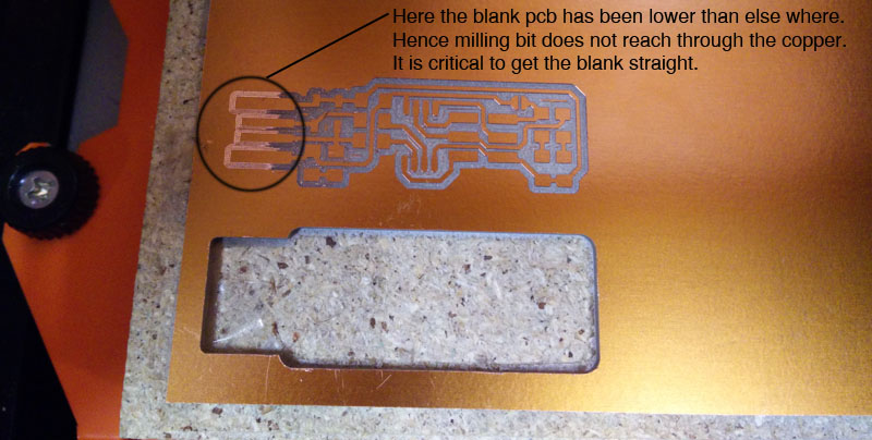
My first couple of millings did not go well but 3th time's the charm and I got one well milled pcb. On the first failed milling the blank pcb was not level, so part of the milling did not happen. See the picture.
Soldering the components on i.e. assembling the board
All the components were available FabLabs storage. It is time to do some soldering.
List of all components needed for this board. I used ATtiny45.
- 1x ATtiny45 or ATtiny85
- 2x 1kΩ resistors
- 2x 499Ω resistors
- 2x 49Ω resistors
- 2x 3.3v zener diodes
- 1x red LED
- 1x green LED
- 1x 100nF capacitor
- 1x 2x3 pin header
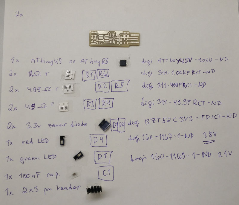
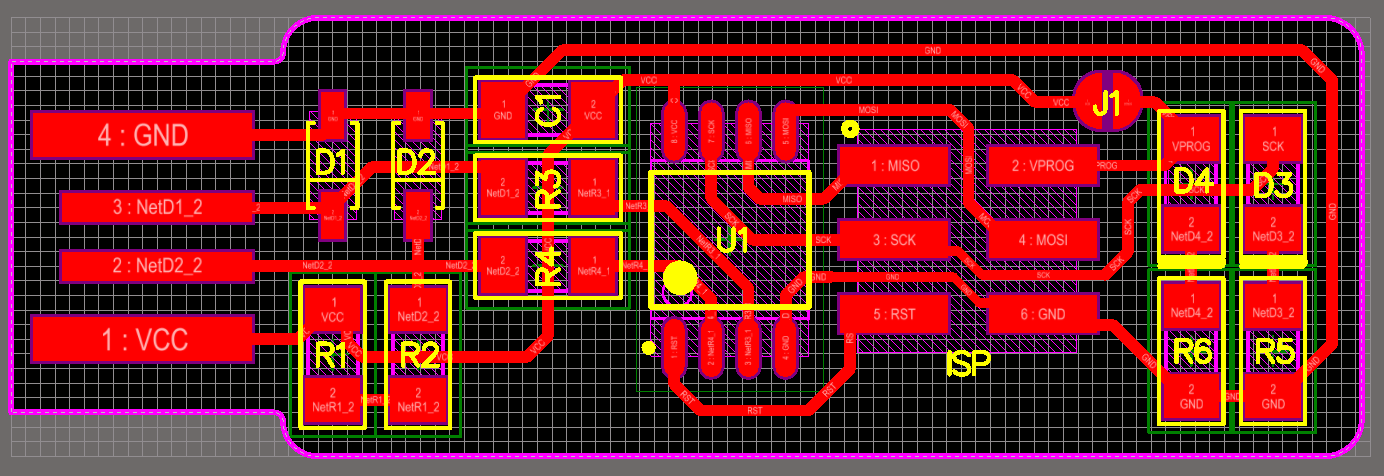
Picture of component placement here. Component designation is visible on the collected components picture.
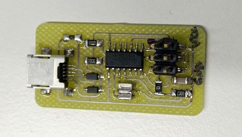
And here is the ready made board.
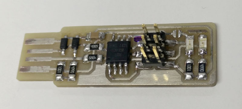
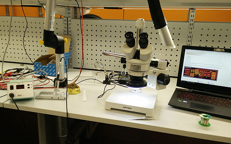
Soldering is familiar to me, so it did not take a lot of time to finish this. I love to see what happens when soldering so I use microscope and good fine tipped Weller soldering iron. Here is the setup while working on it.
After finishing the first board I wanted to make an other one to test my own programmer. I selected one called FabOptimus by Ali. I used my work place PCB milling process for that. The milling machine is LPKF S103 milling/drilling machine. I will not go into detail in that as it is not stantard FabLab process. After milling I but the components on and then it was time to start programming. Of course I programmed the first board with an another programmer from our FabLab. Here is a picture of FabOptimus. There is one annoying feature with FabOptimus. It is using mini-usb connector. It is really hard to find mini-usb nowadays as micro-usb is more of a standard everywhere.
Programming the programmer
After finishing the board, it was time to program it to be a programmer. This was done following the instructions made by Brian. I use windows OS so I had to install some programs from AVR. First it was installing a GIT but that I had already. Then I installed Atmel GNU Toolchain and GNU Make. Finally installing avrdude and then some paths had to be defined for the programs to find software tools installed.
Tasks to get the programming environment going in Windows 10 environment is installing:
1.1. Atmel GNU toolchain. From the selection of programs at the www-page, I got "Atmel AVR 8-bit Toolchain 3.5.4 - Windows" as ATtiny 45 is 8-bit prosessor.
1.2. GNU make. Just note where you install the program, as you will need to make the correct path change later.
1.3. avrdude does not need to install, just add the files to c:/Program files (for example, they can be anywhere).
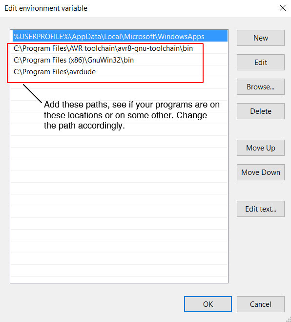
1.4. Adding paths to windows so avrdude will find installed software. Go to Control panel (fast way is to right click mouse button on start-icon) -> System -> Advanced System Settings (on left panel, this will open a new System Properties window) -> Advanced tab -> and click the Environment Variables button in User variables section. Select Path and click the Edit button. Add these three paths. If the path edit does not open new window, use semicolon between the "lines" when adding the paths to path variable. The paths here in this example window are the locations I have my programs. Make sure you select the paths where you added the new software.
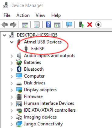
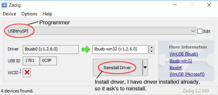
It seems that Windows 10 does not have the right USB-drivers for ISPtiny. I installed the driver using program called Zagid. Plug the programmer (working one, not the one you are about to program) to your usb-port. If windows does not recognize your programmer use zadig to define driver and install it. To see if Windows regognizes your programmer go to Cotrol panel -> System -> Device manager (again on the left). This will open Device Manager window. Your Programmer should be listed as Atmel USB Devise-FabISP (in my case).
If you do not find your programmer, run the Zadig.
Next you can test that the software work and the paths are correct. Please follow good instructions at Brians page here. Just go to the "Sanity Check" part at the end of the page.
Flashing the ATtiny... finally
Programming started with downloading the source code and compiling it to .hex file that will be programmed to the new boards atmega-chip. It was done by downloading the source from
here. Open your console (git bash or so) and go to the folder you downloaded the sofware files. Write make and the .hex file is generated.
Next was time to connect the hardware and program the new system. This was done by plugging the programmer to computer USB port. connecting the programming cable to the new board. On my case power for the new board was provided by the programmer hence there is no need to get any other power source to the new board. In case you need to add power to the new board, it can be given from other USB-port or separate power source.
Following the instrucions at Brians page I opened the git bash console and run the
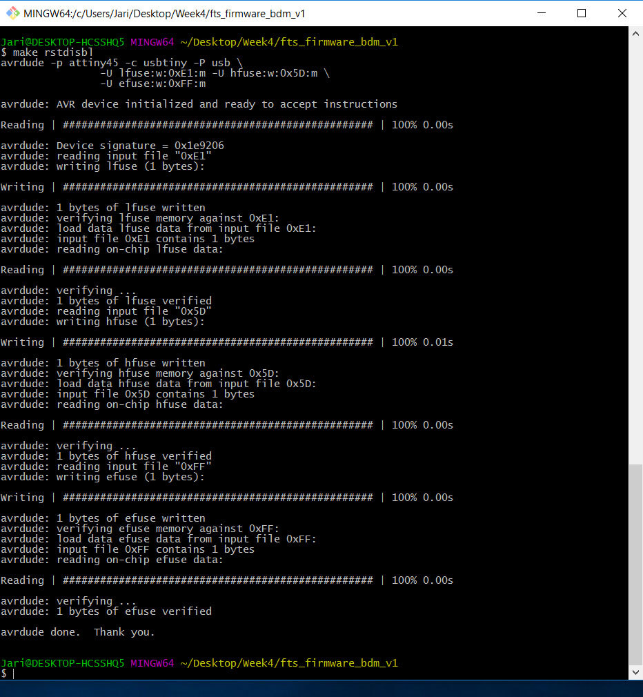
1. First we generate the program file (.hex) that can be loaded to the microcontroller using command Make.
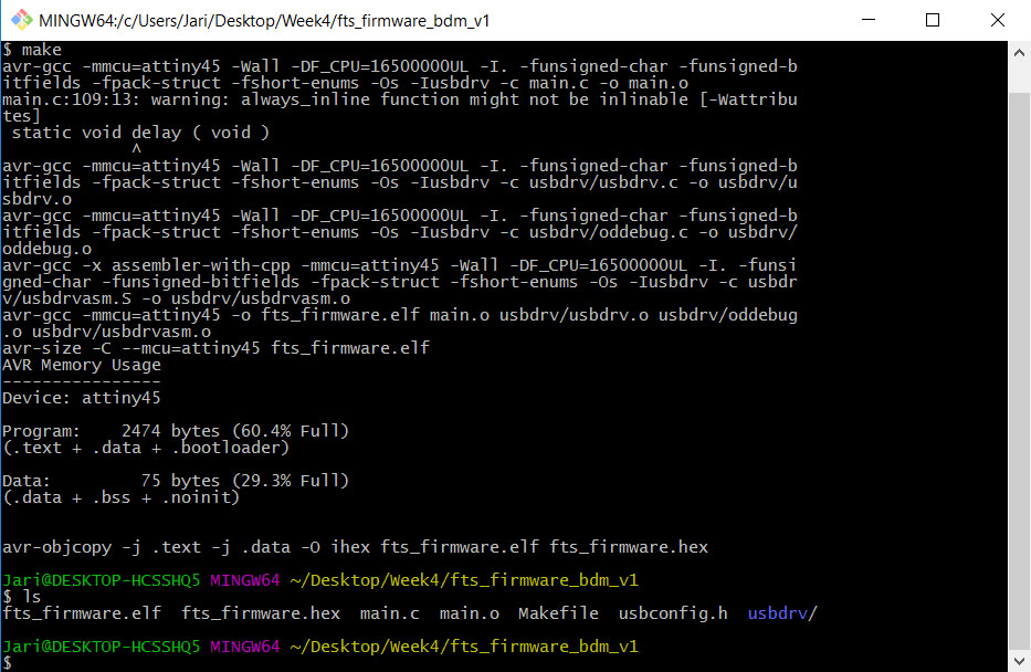
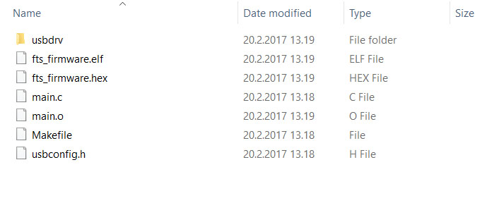
There is a better visualization of files generated.
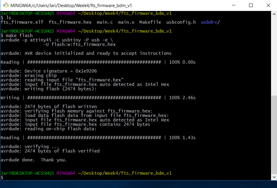
2. make flash; this will program the .hex file compiled earlier to the chip.
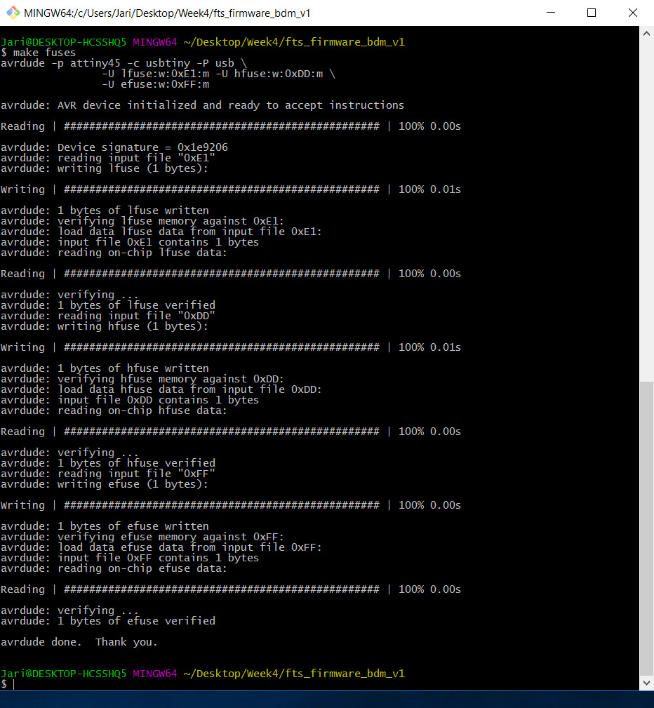
3. make fuses; Make the fuses except the one that makes chip not possible to program again. (Makes reset pin as normal IO-pin.)
4. Before blowing the reset fuse, its time to test if the new programmer works. Unplug programmers and plug the new one to your computers usb port, if it shows in windows as usb-devise (see instructions above to see if you board is recognised by the OS. If it does not show up, start debugging with Brians instructions. On my case it worked well, so I just went on blowing the reset fuse.
5. use command make rstdisbl and that will do it. Now the new board is ready to be used as a programmer.
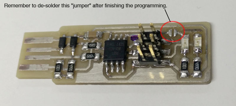
Oh and the last thing, remember to de-solder the bridge made to the board. See picture. It is de-soldered here already.
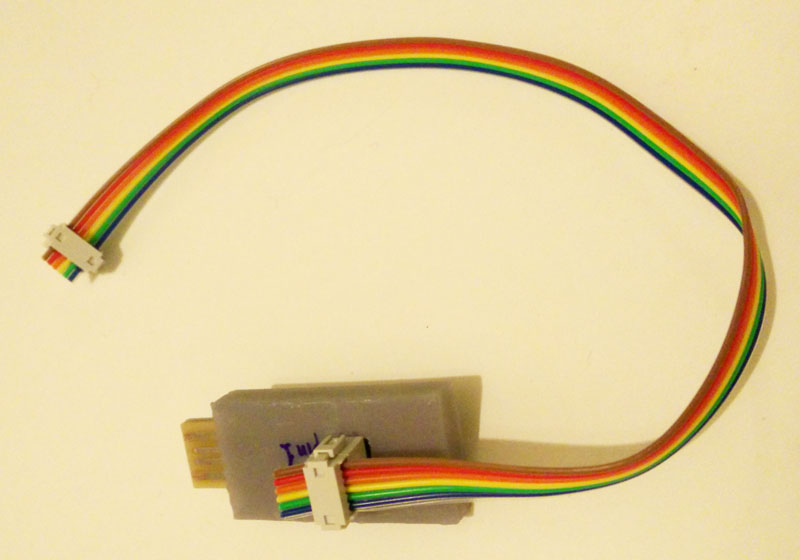
At the end I also made this cable and small case for the board with one of our 3D-printers. Links to the files are behind the i-symbol at the bottom of the page.
Tools, machines and software used during this weeks assingment:
1. FabLab milling machine: Roland SRM-20 and its software interface VPanel for SRM-20
2. Soldering iron. Weller WMRS (not FabLab stardard), but with a fine tip
3. Windows OS AVR programming environments:
3.1. Atmel GNU toolchain.
3.2. GNU make
3.3. avrdude
Files used with this weeks assignment
Here are the files. All of them this week are not done by me, but downloaded from others. Later in the text, when I talk about the process, the links to the source pages are given.
Traces.PNG file
Outline.PNG file
Test cut file made from outline-file
Traces milling file made with fabmodules
Outline milling file made with fabmodules
3D printed case bottom part for the programmer CAD-file
3D printed case bottom part for the programmer .STL-file
3D printed case top part for the programmer CAD-file
3D printed case top part for the programmer .STL-file