Assignment 13
26.4.2017
Topic: Input devices
Measure something: add a sensor to a microcontroller board that you
have designed and read it.
Learning outcomes:
Demonstrate workflows used in circuit board design and fabrication.
Implement and interpret programming protocols.
Have you:
Described your design and fabrication process using
words/images/screenshots.
Explained the programming process/es you used and how the
microcontroller datasheet helped you.
Explained problems and how you fixed them.
Included original design files and code.
A/D conversion (ADC)
Analog-to -digital conversion is totally new thing for me. I was
interested to study it and use it in my final project. For example,
Attiny44 has 10 bit resolution of ADC and 8 channels. As my final
project, I want measure two things, supply voltage (12 V) of my car
battery and temperature inside the car.
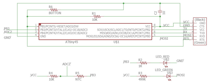
I designed a simple test board it include two voltage dividers: One
use 2x100k resistors to drop voltage from maximum 15 V to Attiny44's
measurable level 5 V on ADC pin and then 100k resistor from ADC pin
to ground. The second use 10k resistor from 5 V to ADC pin and from
there NTC thermistor to ground. NTC type is NAQ103B 375T10. Thus,
it's parameters are R25 10 kΩ and B (25/85) 3750. Bridge circuit
might be more accurate but voltage divider is enough in my use. I
detect only one limit temperature.
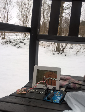
I milled this PCB board and put components and wires in place. I
measured some basic tests to test the board and understand it's
working. Voltage on ADC pin decreases when temperature increases.
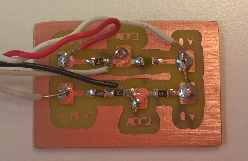 Wires in top side:
Red: +5 V
White: 0 V
Wires in bottom side:
White: +12 V
Black: ADC 2, voltage
White wire in middle: ADC 1, temperature
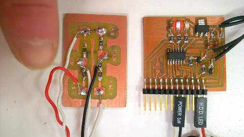
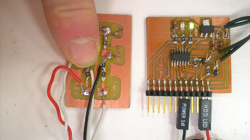
I designed the board so that I can connect it to the output board I
made as Assignment 10. Similarly
maybe, I need input device connected to main board in my final
project. I wrote some code for it. I got some help from page:
https://www.marcelpost.com/wiki/index.php/ATtiny85_ADC. ATTINY44
data sheet advices that by default, the successive approximation
circuitry requires an input clock frequency between 50 kHz and 200
kHz to get maximum resolution.
I can select ADC channel by MUX values. ADMUX = 000011b changes it
as pin PA3/ADC3.
Prescaler is here 64, therefore sample rate is about 15 kHz for 1
MHz clock. Prescaler should be 16 for 62.5 kHz
sample rate.
I used here 8 bit ADC, therefore the maximum ADC value was 255.
If the ADC value is less than 128, the green led lights and if it is
more the red led lights.
Then, I made a finger test. My finger warmed the NTC and led color
changes from red to green.
I tested my board with Arduino also. It has also 10 bit ADC. This
simple program reads ADC pin and print it out.
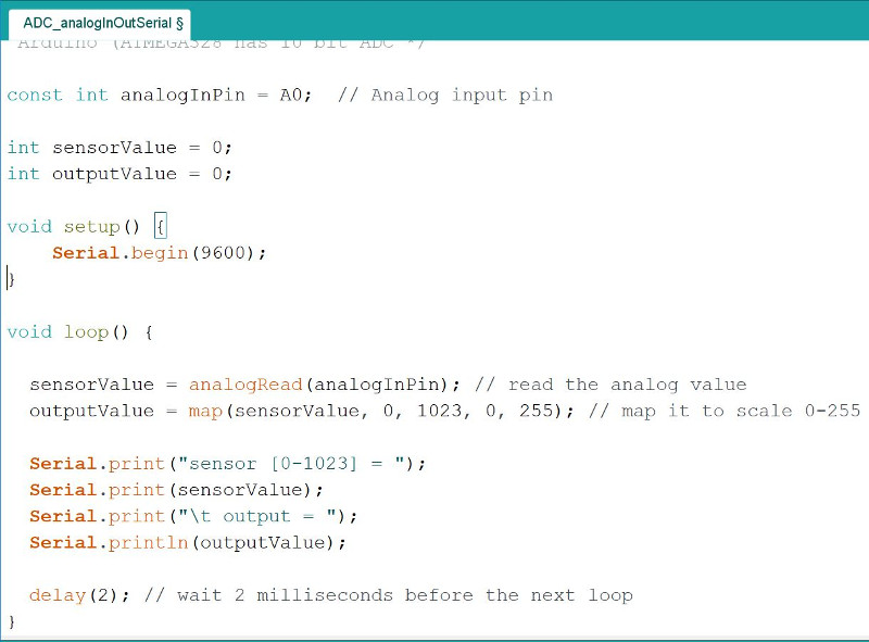
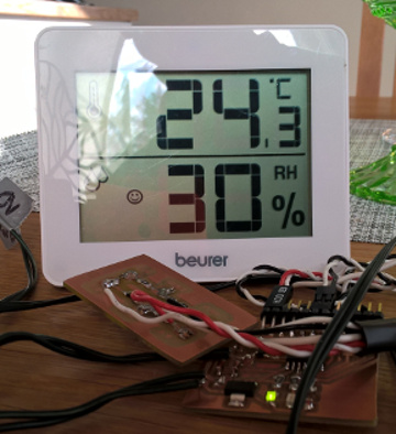
Room temperature at 24.3 °C gives ADC value 128 at scale 0-255.
Voltage level is 2.57 V. Outside temperature at 2.4 °C gives
ADC value 179 at scale 0-255. Voltage level is 3.54 V.
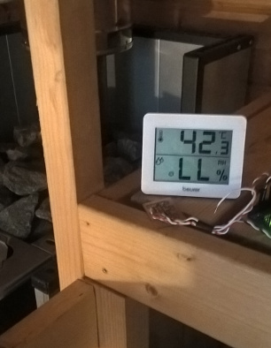
Warming sauna temperature at 42 °C gives ADC value 95 at scale
0-255. Voltage level is 1.88 V.
Further, I measured following data. Temperature (down) increased
from +8 °C to +42 °C. I documented Adc values (left) and voltages
(right). The reference voltage was set to VCC, 5.04 V.
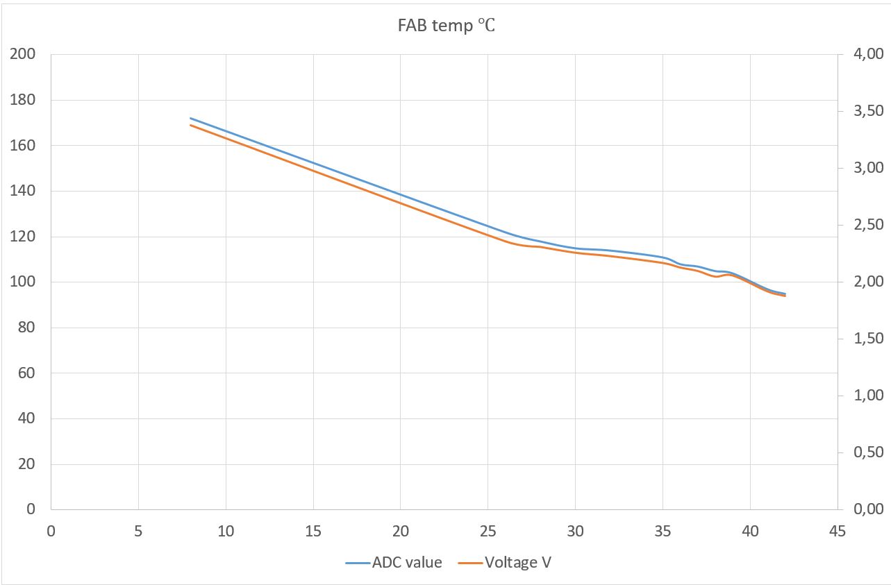
Thus, ADC value decreases when temperature increases as planned. The
curve is very linear from temperature 8 °C to 26 °C, because I
measured only two temperatures there. Between 26 and 42 °C I
measured values as 1 to 2 °C steps.
I want measure two channels as my final project and I wrote
following code for it.
// FAB_ADC02.c This code is edited by Yrjo L. for Attiny44 use
2.5.2017
// ====================================
//
ATtiny44
ISP
//
VCC--+ o
+--GND
MISO---+5V
// GREEN LED PB0
--+ +--PA0
M2 SCK
---MOSI
// RED LED PB1
--+ +--PA1
M1 RST
---GND
THIS IS
NOT THE FINAL CODE FOR FINAL PROJECT
//
RESET
--+ +--PA2 ADC2
//
INT0 PB2 --+ +--PA3 ADC3
TEMP
//
PA7 --+ +--SCK ADC4
V-MEA
//
MOSI --+--------+--MISO
// ====================================
#define F_CPU 1000000UL // 1 MHz (UL Unsigned
Long)
#include <avr/io.h>
#include <util/delay.h>
#define LED_RED PB1
// Define the I/O port to be
used for the RED LED.
#define LED_GREEN PB0 // Define the I/O port to
be used for the GREEN LED.
// #define MOTOR1 PA1 //
Define the I/O port to be used for the MOTOR 1.
// #define MOTOR2 PA0 //
Define the I/O port to be used for the MOTOR 2.
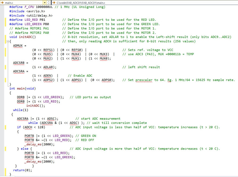
void initADC()
// 8-bit resolution, set ADLAR to 1 to enable the Left-shift
result (only bits ADC9..ADC2)
{
// then, only reading
ADCH is sufficient for 8-bit results (256 values)
ADCSRB = (1 <<
ADLAR);
// left
shift result
ADCSRA = (1 << ADEN)
| // Enable ADC
(1 << ADPS2);
// Set prescaler to 16. Eg. 1
MHz/16 = 62.5 Hz sample rate.
}
int main(void)
{
int Mtemp;
int Mvolt;
DDRB |= (1 << LED_GREEN);
// LED ports as output
DDRB |= (1 << LED_RED);
initADC();
while(1) {
ADMUX = (1 << MUX1) | (1
<< MUX0); // use ADC3 (PA3), MUX
=000011b = TEMP
ADMUX &= ~(1 <<
MUX2);
// not use ADC4 (PA4) MUX =000100b = VOLTAGE
ADCSRA |= (1 <<
ADSC);
// start
ADC measurement =TEMP
while (ADCSRA & (1
<< ADSC) );
// wait till conversion complete
Mtemp = ADCH;
_delay_ms(2000);
ADMUX &= ~(1 << MUX1) & ~(1
<< MUX0); // not use ADC3 (PA3), MUX =000011b = TEMP
ADMUX = (1 << MUX2);
// use ADC4 (PA4) MUX =000100b
= VOLTAGE
ADCSRA |= (1 <<
ADSC);
//
start ADC measurement =VOLTAGE
while (ADCSRA & (1
<< ADSC) );
// wait till conversion
complete
Mvolt = ADCH;
if (Mtemp < 128 || Mvolt < 200)
// if temperature > 20C or
voltage < 12V then pump and blower stop
{
PORTB |= (1 <<
LED_GREEN); // pump & blower stop
PORTB &= ~(1 << LED_RED);
_delay_ms(2000);
} else {
// if temperature < 20C and voltage >
12V then pump and blower work
PORTB |= (1 <<
LED_RED); // pump & blower
start
PORTB &= ~(1 <<
LED_GREEN);
_delay_ms(2000);
}
} return(0);
}
It works as expected. If temperature is more than 20 °C or battery
voltage is lower than 12 V, then the pump and blower stops and GREEN
led lights. Battery voltage level 11.8 V refers to ADC value >
200 and then ADC voltage level is 3.91 V. Voltage level 11.7 V
switches RED led on. It refers to to ADC value of < 200 and then
ADC voltage level is 3.88 V. Those limits are ideal, however. ADC
value of 138 might suit better for temperature limit 20 °C.
ADMUX = 000011b changes pin PA3/ADC3 and ADMUX = 00100b changes pin
PA4/ADC4 as the ADC channel.
Prescaler is here 16, therefore sample rate is 62.5 kHz for 1 MHz
clock as recommended in data sheet.
Motors 1 and 2 are not yet coded anymore here.
Design files: NTC+15V.sch and CTN+15V.brd.
Code: FAB_ADC02_main.c.
Board as png file: NTC+15VTRC.png.
As replacement of a output file I tested drive outlines by manual
control.
Post-registered note:
Later, I made similar voltage dividers for my final project use. Node_F1
board measures temperature and MainB_F1 voltage.
Node_F1
During assignment 15,
networking and communication, I made a board for communication but
also for testing of temperature measurement (ADC), user interface
and serial communication together. My original ADC code needed some
modifications to work also in Attiny45. One difference
exists as ADLAR set in ADMUX |register for attiny45 and ADCSRB
register for Attiny44.
Further, pin PB3 control both the RED led and ADC measurement
/ADC2). When it is 1, led lights, and when it is 0, temperature
measurement circuit grounds via PB3 and starts. Green led is
controlled by pin PB0. I added also a button to test RESET pin
feature.
This schematic is for Node_F1.
I must change pins TX and RX that I can use direct cable between
units.
MainB_F1
As well as during final project
I made MainB_F1 board as a evolution of boards made during
assignment 10 and 13. It is presented below and includes voltage
measurement by ADC (ADC7).
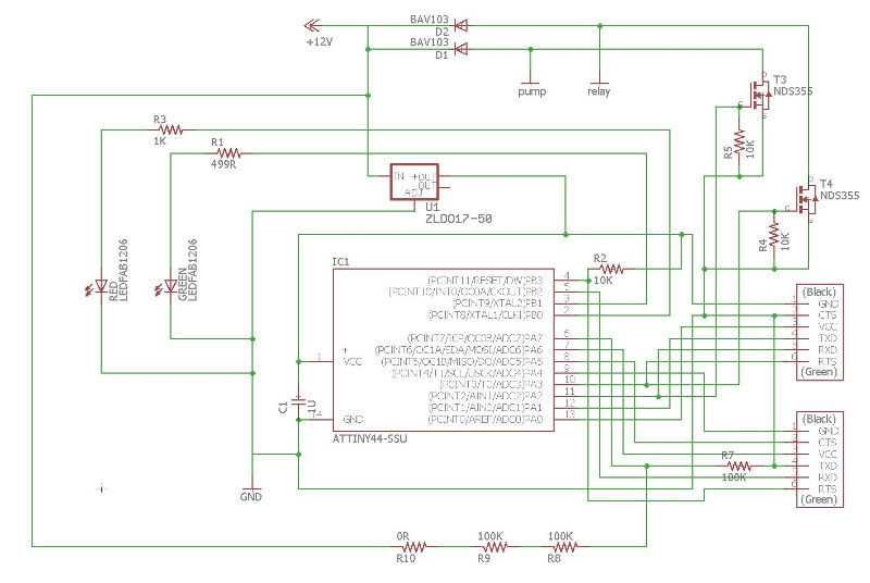
This schematic is for MainB_F1.
Boards as png files: fabnode_track02.png
and FABcamper21.png.