Embedded Programming
Introduction
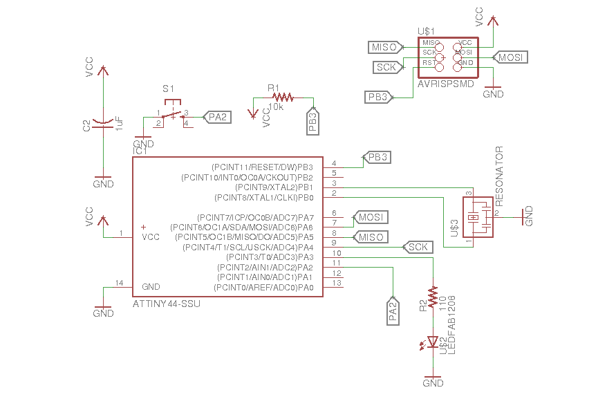
In the introduction section i will mention some information about the Micro controller ATTiny44 witch is the one we are using in the lab. ATTiny24/44/84 are all the same by having 14 pins with the difference in the memory. ATTiny45 have 8 pins, so basically we choose the type of the Micro controller based on the number of pins we are utilizing while we build our own circuit board.
Back to ATTiny44, ATTiny44 have 14 pins, some of the pins are control pins while others are free pins that for example can be connected to our input and output devices.
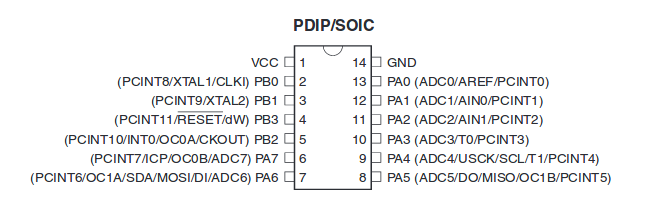
Now lets understand some of the control pins that we will be using in the lab. These pins are: Vcc, GND, MOSI, MISO, RST and SCK. I will briefly describe each of these pins. Vcc is providing voltage to the circuit from the Vcc pin in the controller and GND is grounding the circuit board or any other element connected to the ground. MOSI is master Data output, Slave Data input and MISO is master Data input, Slave Data output, But, they are just inputs/outputs and can be programmed to do almost anything. SCK is Universal Serial Interface Clock and RESET is External Reset input is active low and enabled by unprogramming (“1”) the RSTDISBL Fuse.
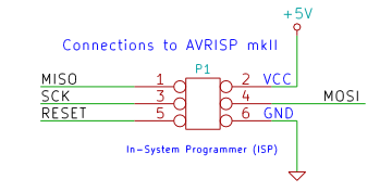
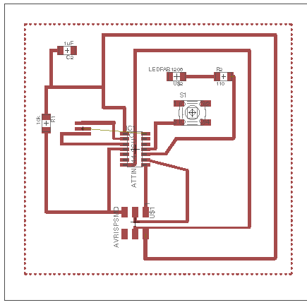
The mentioned above control pins are connected to an AVR 2x3 header as shown below. The 2x3 Header is connected to a programmer with the same control pins from the programmer side. The same pins supply the microcontroller with voltage and upload the program at the same time.
Moreover, ATTiny24/44/84 has 2/4/8 K Bytes of Programmable Program Memory Flash and requires a power of around 5 Volts. Below are the full features of ATTiny24/44/84:
• High Performance, Low Power AVR ® 8-Bit Microcontroller
• Advanced RISC Architecture
– 120 Powerful Instructions
– Most Single Clock Cycle Execution
– 32 x 8 General Purpose Working Registers
– Fully Static Operation
• Non-Volatile Program and Data Memories
– 2/4/8K Bytes of In-System Programmable Program Memory Flash
• Endurance: 10,000 Write/Erase Cycles
– 128/256/512 By tes of In-System Programmable EEPROM
• Endurance: 100,000 Write/Erase Cycles
– 128/256/512 Bytes of Internal SRAM
– Data Retention: 20 years at 85 ° C / 100 years at 25 ° C
– Programming Lock for Self-Programming Flash & EEPROM Data Security
• Peripheral Features
– One 8-Bit and One 16-Bit Timer/ Counter with Two PWM Channels, Each
– 10-bit ADC
• 8 Single-Ended Channels
• 12 Differential ADC Channel Pairs with Programmable Gain (1x / 20x)
– Programmable Watchdog Timer with Separate On-chip Oscillator
– On-chip Analog Comparator
– Universal Serial Interface
• Special Microcontroller Features
– debugWIRE On-chip Debug System
– In-System Programmable via SPI Port
– Internal and External Interrupt Sour ces: Pin Change In terrupt on 12 Pins
– Low Power Idle, ADC Noise Reductio n, Standby and Power-Down Modes
– Enhanced Power-on Reset Circuit
– Programmable Brown-out Detection Circuit
– Internal Calibrated Oscillator
– On-chip Temperature Sensor
• I/O and Packages
– Available in 20-Pin QFN/ MLF & 14-Pin SOIC and PDIP
– Twelve Programmable I/O Lines
• Operating Voltage:
– 1.8 – 5.5V for ATtiny24V/44V/84V
– 2.7 – 5.5V for ATtiny24/44/84
• Speed Grade
– ATtiny24V/44V/84V
• 0 – 4 MHz @ 1.8 – 5.5V
• 0 – 10 MHz @ 2.7 – 5.5V
– ATtiny24/44/84
• 0 – 10 MHz @ 2.7 – 5.5V
• 0 – 20 MHz @ 4.5 – 5.5V
• Industrial Temperature Range: -40 ° C to +85 ° C
• Low Power Consumption
– Active Mode (1 MHz System Clock): 300 μA @ 1.8V
– Power-Down Mode: 0.1 μA @ 1.8V"
This Week Work
In this week, the task is to install a program in our developed circuit board in week 6. The program should utilize the installed LED and Switch. In this regards, I went through and read about the programming codes from Arduino website and some web fourms. So I had a general understating as follows:
1- The code will consists of two main fuctions void setup() and void loop ().
2- in void setup() you define the input and output pins the will be read from the microcontroller. For example pinMode(0, OUTPUT); //LED & pinMode(1, INPUT); //Switch. Assuming in the previos example LED ais connected PA0 and Switch is connected PA1.
3- in the viod loop () you write the code related to the outputs elements behaiver. For example:
if(1,HIGH)// SWITCH PRESSED
{
int repeat_end = 4;
for (int count = 0; count < repeat_end; count++)
{
digitalWrite(0,HIGH);
delay (2*1000);
digitalWrite(0,LOW);
delay(2*1000);
}
}
}
"
The code means that if the switch is clicked, the LED will blink for 2 seconds and goes off for 2 seconds four times. DigitalWire n this case force to set the pin voltage to high or zero.
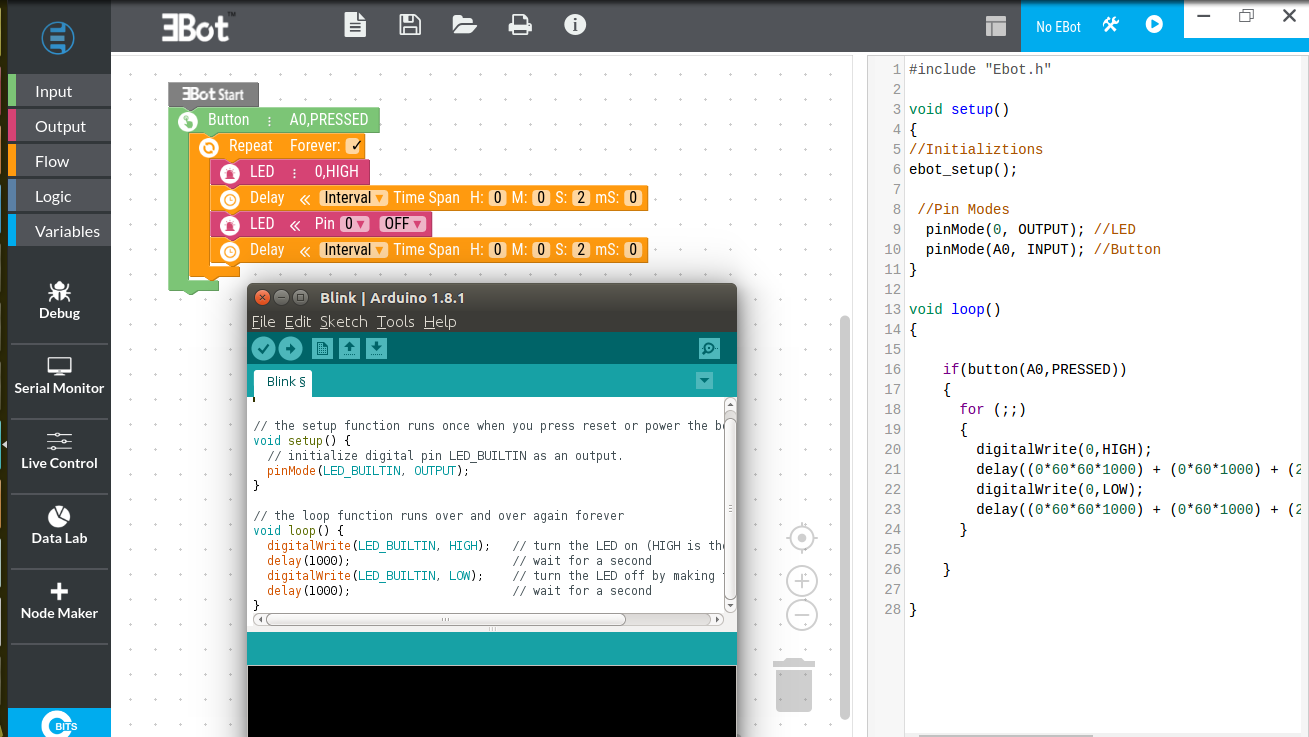
our instructor had also introduced a built in application known as Ebot or as known earlier snow ball. This application translate a GUI design into a code understandable by Arduino. Example shown below.
Programming The Board
I had printed 2 circuit boards with the same schematic design but defferent BRD traceses. when I connected the first board to the programmer. I tested the blinking LED Code which is on and off for 1 second each. and it worked.
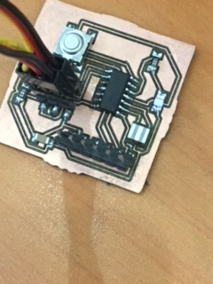
I tried again after 30 minuts to document but i had an RC-1 ERROR "check your connection". I went and tested the second Circuit board but it was not working "same connection error". I thought instead of debugging the second board i will make new circuit board with defferent schematic design. I created my third borad, soldered all the elements -> connected it to the programmer -> upload the programm -> and blinking worked. Changed the programm and included the switch without moving the board -> RC-1 error "check your connection". that was depressing. I spoked to Mr. Francisco and he advised to create a debugging table. so, i chose the second board and made a debugging list.
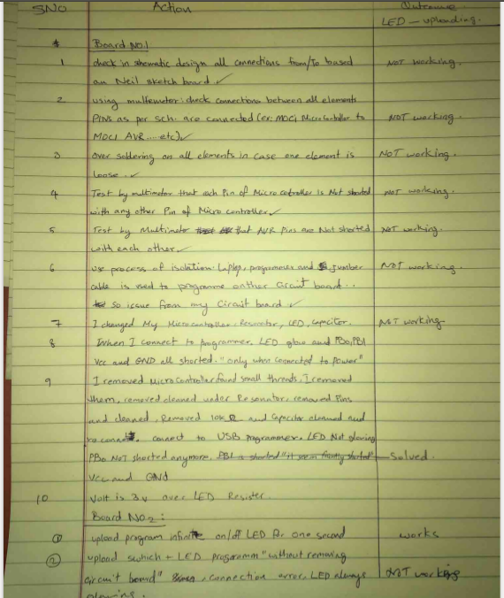
During testing i connected by mistake the GND cable jumber to VCC and burned the microcontroller. i replaced the Microcontroller and upluaded the programm and it worked. but, if I use the intenal crystal of the microcontroller the blinking timing is done correctly based on the code. but if i use the 20 MHz resonator the timing increase. Therefore, I went to http://www.engbedded.com/fusecalc/ and tried to change the microcontroller fuses to fix the timing. but, unfourchantly i missed up the controller. I changed the microcontroller again but i had RC-1 error. I plan to do further check on this issue.
Making It Work
Now in order to make it work. I decided to carefully do each step perfectly to avoid the undesirable situation. So I made sure to do the following:
1- Redo the schematic Design and make sure its correct.
2- Do manual routing instead of auto routing.
3- Reduce number of cables and traces by making the ground on the board surface.
4- During soldering test each element after its soldered.
And it finally work.
int ledPin = 3;
int buttonState = 0;
void setup() {
pinMode(ledPin, OUTPUT);
pinMode(buttonPin, INPUT);
}
void loop() {
buttonState = digitalRead(buttonPin);
if (buttonState == HIGH) {
digitalWrite(ledPin, HIGH); // turn LED on:
} else {
digitalWrite(ledPin, LOW); // turn LED off:
}
}
"
New Board, More Tests
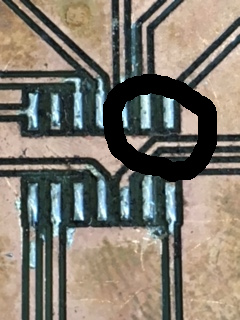
In my design, The plate surface is the GND. For the area surrounding the switch, the only path connecting it to the rest of the GND is underneath the ATTiny 44.
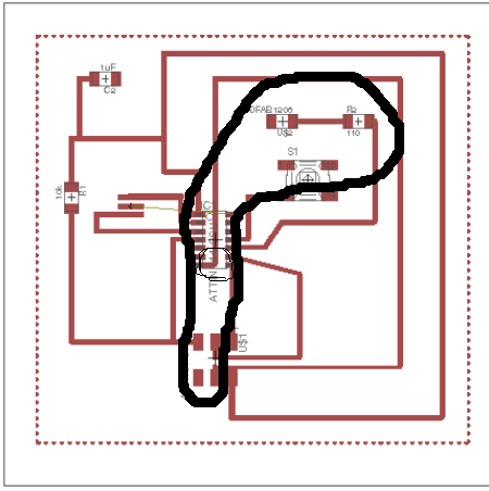
I made a new board and to avoid have very thin routes, I increased the width of the routes. Unfortunately, that caused the only route connecting the ground as shown above to be disconnected.
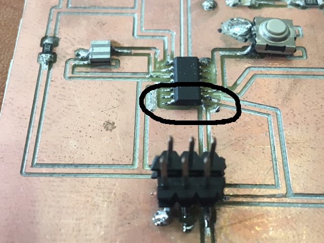
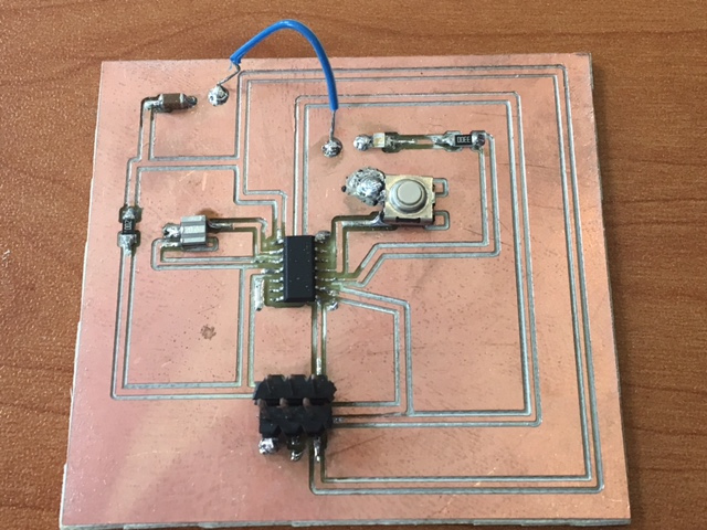
I Joined both the areas with a wire. Soldered the board and tested the Burn BootLoader. Everything was set and ready for programming.
The Code
I tested two different codes to ensure that the board is working, Hereunder are the codes:
Code 1:
the first code works as follows, while the switch is clicked, the LED will blink 4 times even if you keep it pressed.
Code 2:
the second code works as follows, on click the LED will blink 5 times.
Download Files
Debugging List
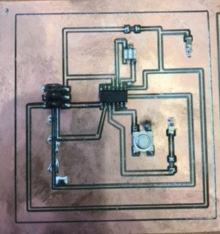
Schematic Design
BRD Design
ATtiny24/44/84 - Atmel Corporation