Embedded Networking and Communications
Introduction
The Inter-integrated Circuit (I2C) Protocol is a protocol intended to allow multiple “slave” digital integrated circuits (“chips”) to communicate with one or more “master” chips. Like the Serial Peripheral Interface (SPI), it is only intended for short distance communications within a single device.
Networking and Communication
Data communications refers to the transmission of this digital data between two or more computers and a computer network or data network is a telecommunications network that allows computers to exchange data. The physical connection between networked computing devices is established using either cable media or wireless media. The best-known computer network is the Internet.
SPI
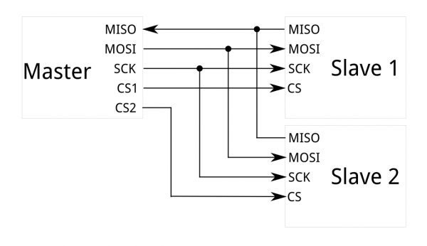
Connecting a single master to a single slave with an SPI bus requires four lines; each additional slave requires one additional chip select I/O pin on the master. The rapid proliferation of pin connections makes it undesirable in situations where lots of devices must be slaved to one master. Also, the large number of connections for each device can make routing signals more difficult in tight PCB layout situations. SPI only allows one master on the bus, but it does support an arbitrary number of slaves
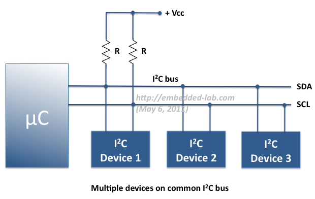
I2C
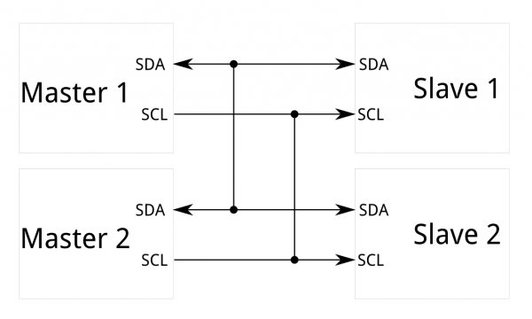
I2C requires only two wires, like asynchronous serial, but those two wires can support up to 1008 slave devices. Also, unlike SPI, I2C can support a multi-master system, allowing more than one master to communicate with all devices on the bus.
I2C History
I2C was originally developed in 1982 by Philips for various Philips chips. The original spec allowed for only 100kHz communications, and provided only for 7-bit addresses, limiting the number of devices on the bus to 112 (there are several reserved addresses, which will never be used for valid I2C addresses). In 1992, the first public specification was published, adding a 400kHz fast-mode as well as an expanded 10-bit address space. Much of the time (for instance, in the ATMega328 device on many Arduino-compatible boards) , device support for I2C ends at this point. There are three additional modes specified: fast-mode plus, at 1MHz; high-speed mode, at 3.4MHz; and ultra-fast mode, at 5MHz. In addition to “vanilla” I2C, Intel introduced a variant in 1995 call “System Management Bus” (SMBus). SMBus is a more tightly controlled format, intended to maximize predictability of communications between support ICs on PC motherboards. The most significant difference between SMBus is that it limits speeds from 10kHz to 100kHz, while I2C can support devices from 0kHz to 5MHz. SMBus includes a clock timeout mode which makes low-speed operations illegal, although many SMBus devices will support it anyway to maximize interoperability with embedded I2C systems.
My Work for this Week
I plan to use a master Micro processor and two slave Micro processors installed each with LED. I have create the schematic files for the three boards (Attached in footer), generated the BRD file and printed the boards.
after Soldering all the three boards, I connected all the circuit boards with a bread board in order to link TX and RX interfaces.
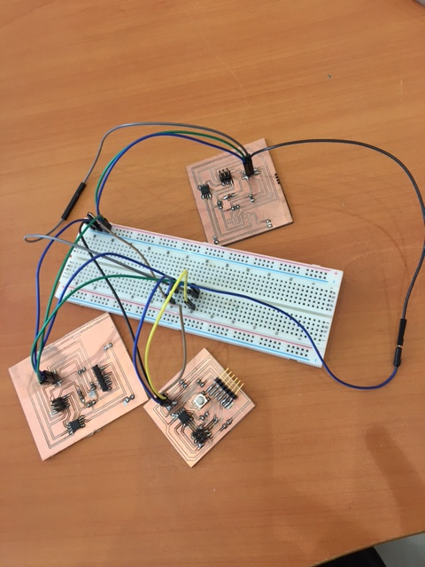
In order to set the master and slaves it is required to set manually the address of the slaves. Therefore, I set manually the address of both boards to 0x1 and 0x2. Then the master board starts the transmission by calling both mentioned addresses.
I used the following code:
For Master Circuit Board:
void setup()
{
TinyWireM.begin(); // join i2c bus (address optional for master)
}
byte x = 0;
byte x1 = 0;
void loop() {
TinyWireM.beginTransmission(0x1);
TinyWireM.write(++x % 2);
TinyWireM.endTransmission();
delay(1000);
TinyWireM.beginTransmission(0x2);
TinyWireM.write(++x1 % 2);
TinyWireM.endTransmission();
delay(1000);
}"
For Slave Circuit Board:
#define input(directions, pin) (directions &= (~(1 << pin))) // set port direction for input
#define set(port, pin) (port |= (1 << pin)) // set port pin
#define clear(port, pin) (port &= (~(1 << pin))) // clear port pin
#define LED_PIN PB4
#define I2C_SLAVE_ADDRESS 0x1 // Address of the slave 1
#include
void setup()
{
output(DDRB, LED_PIN);
clear(PORTB, LED_PIN);
TinyWireS.begin(I2C_SLAVE_ADDRESS); // join i2c network
}
void loop()
{
byte recd = 1;
if(TinyWireS.available()) {
recd = TinyWireS.receive();
if(recd == 1) {
clear(PORTB, LED_PIN);
} else {
set(PORTB, LED_PIN);
}
}
}"
Issues Faced
1) I thought "Wire" would work on ATTiny but it didnot after some research on the internet i knew about TinyWire Library.
2) The first Two slaves i made had a design flow. I did connect TX and RX pins to 10K resister each but i did not connect each to VCC. unfortunately i noticed this after soldering the two boards.
3) In order to experiment a lot of componants, I planned to user Ultrasonic in the Master Board and Buzzer + LED in the save Boards. After Soldering, Ultrasonic and Buzzer Boards had connection error during burning the bootloader. debugging would be a time consuming "You may refer to my week 8 for more details". So, I changed the Ultrasonic for Switch button and Buzzer to LED.
4) After Testing the Master Board without Switch, I was already Late for the Interface and Application Programming. Therefore, I concluded this week with the video above. If i have time later i will do further testing and update this page.
Downloaded files
Master Board Schematic
Master Board BRD
Slave One Board Schematic
Slave One Board BRD
Slave Two Board Schematic
Slave Two Board BRD