Week 06
Electronics Design

The sixth lecture on Wednesday March the 1st was about Electronics Design: from components to circuits: it was also the first time official introduction to EDA software through the presentation of different tools. Assignment given by Neil for this sixth week was about selecting and using software for circuit board design and demonstrating workflows used in circuit board design itself:
- Redraw the echo hello-world board adding (at least) a button and LED (with current-limiting resistor)
- Check the design rules, make it and test it
Redrawing the echo hello-world board
Being at my very first electronic-design experience, after a deep websearch about some of the different EDA software tools presented by Neil during his lecture I was initially attracted by Eagle, one of the industry standards recently acquired by Autodesk, but I ended choosing KiCAD. KiCAD was originally developed in 1992 by Jean-Pierre Charras, and now has notable contributors such as CERN; it features an integrated environment for schematic PCB layout design. Despite the fact that KiCAD is not yet considered on par with commercial EDA tools and sometimes not suggested for absolute-beginner experiences cause the lack of documentation, I found very simple to learn and on the official website there's also a dedicated sections with links to some good tutorials. What made me go for KiCAD is mainly being distributed with under the terms of the GNU/GPLv3+ license: as far as I can, I prefer using a Free Software and a GNU/Linux system.
KiCAD software can be downloaded from official website or from the online software repositories of the main GNU/Linux distributions; in a Debian or derivatives (e.g. popular Ubuntu and Mint distributions), it's easy as opening a terminal and using apt-get package manager:
~ $ apt-get install kicad
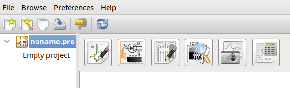
KiCAD has different software modules. Basic workflow in KiCAD is:
- Create a project
- Create a schematic with Eeschema
- Assign footprints to symbols and generate the netlist
- Create a board with PcbNew, importing the netlist from 'eeschema'
- Test the board using the DRC
- Generate production files
Let's start opening KiCAD main interface
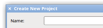
Creating a New Project
brings to Eeschema module
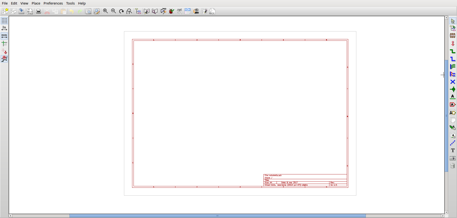
and to the main Eeschema workspace
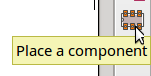
First of all I tried to design simple circuits placing a New Component
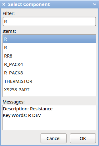
Selecting from a list, in this case a resistor (R)
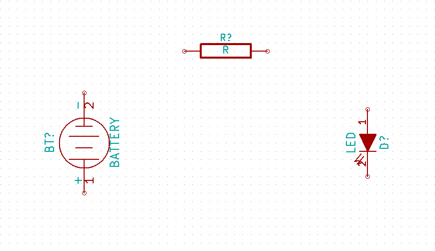
Once all the components are on the workspace
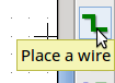
it's possibile to place wires to create links between them (wires then become tracks on PCBs)
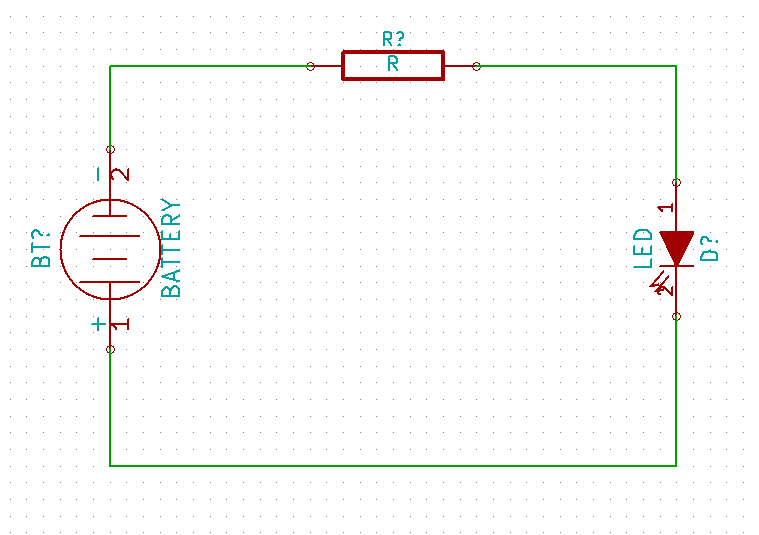
(...wiring in progress...) / 1 -battery-to-resistor
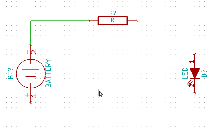
(...wiring in progress...) / 2 -resistor-to-LED and LED-to-battery
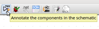
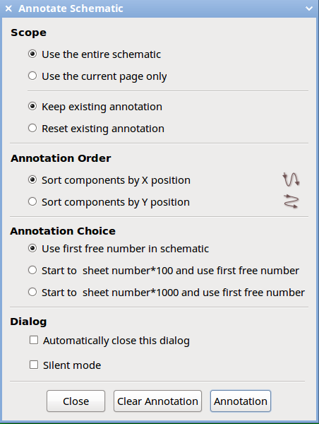
in order make easier wiring connections, it's possible to annotate the component in the schematics
between the options, it's possible to select annotation order and choice
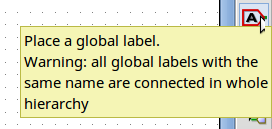
then it's possibile to place Labels (small note-to-self about "style": as pointed out by guru instructor Bas Withagen during global review process, it´s ok to use labels for longer lines, but maybe not for every signal, as it will make a schematic harder to read; also VCC and GND have special symbols in the component libraries that are preferred to be used over labels or direct connections)
for instance, placing "LED" at the end of two wires, makes KiCAD refer to them as the same wire
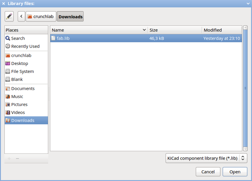
Fab Inventory parts can be found loading the external "fab.lib" electronic component library
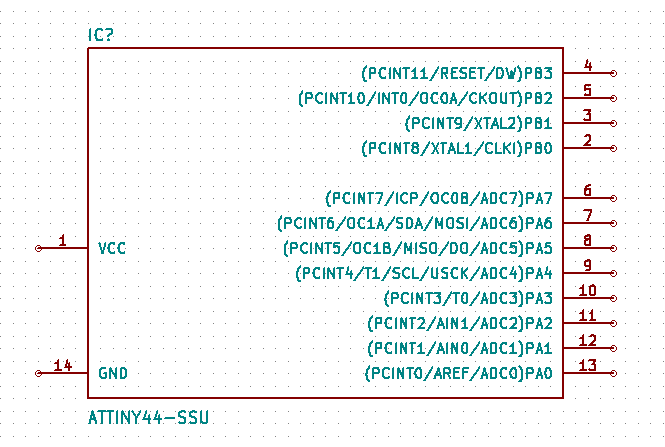
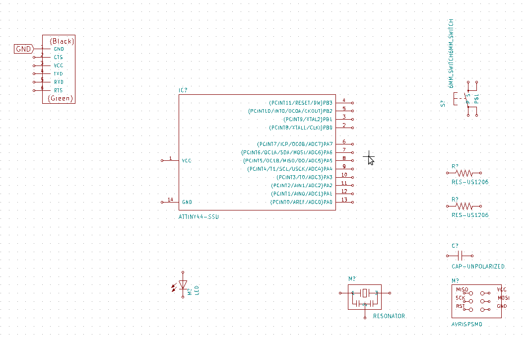
here's schema for ATTiny 84-SSU microcontroller (with all his pins and ports)
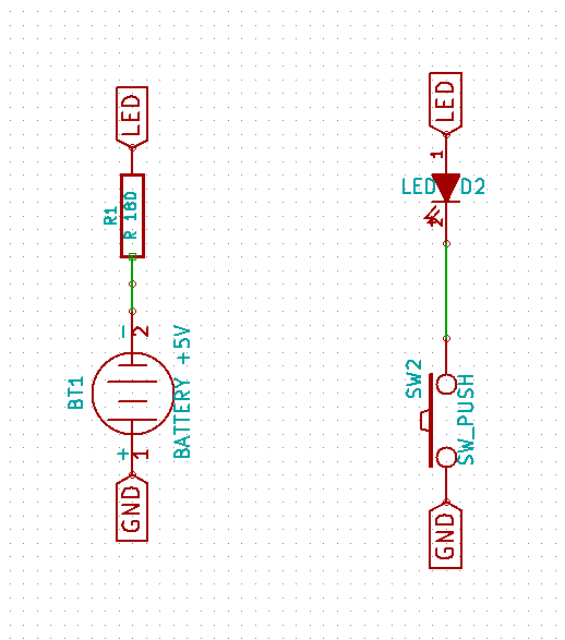
Time to go to echo-hello board re-design! Placing all the needed electronic components on the schema (ATTiny 84-SSU, resonator, LED, switch, resistors, capacitor, pin-headers)
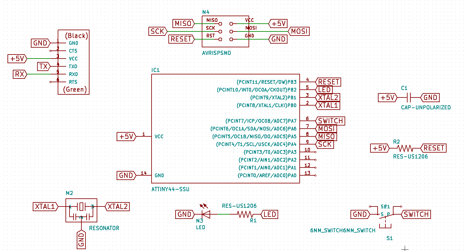
Organizing electronic components and placing wires and labels, including a button switch and a LED with current-limiting resitor.
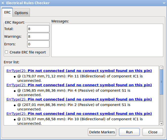
Clicking the ladybug icon to perform Electrical Rules Check
(...no relevant errors found...) / 1 -schema
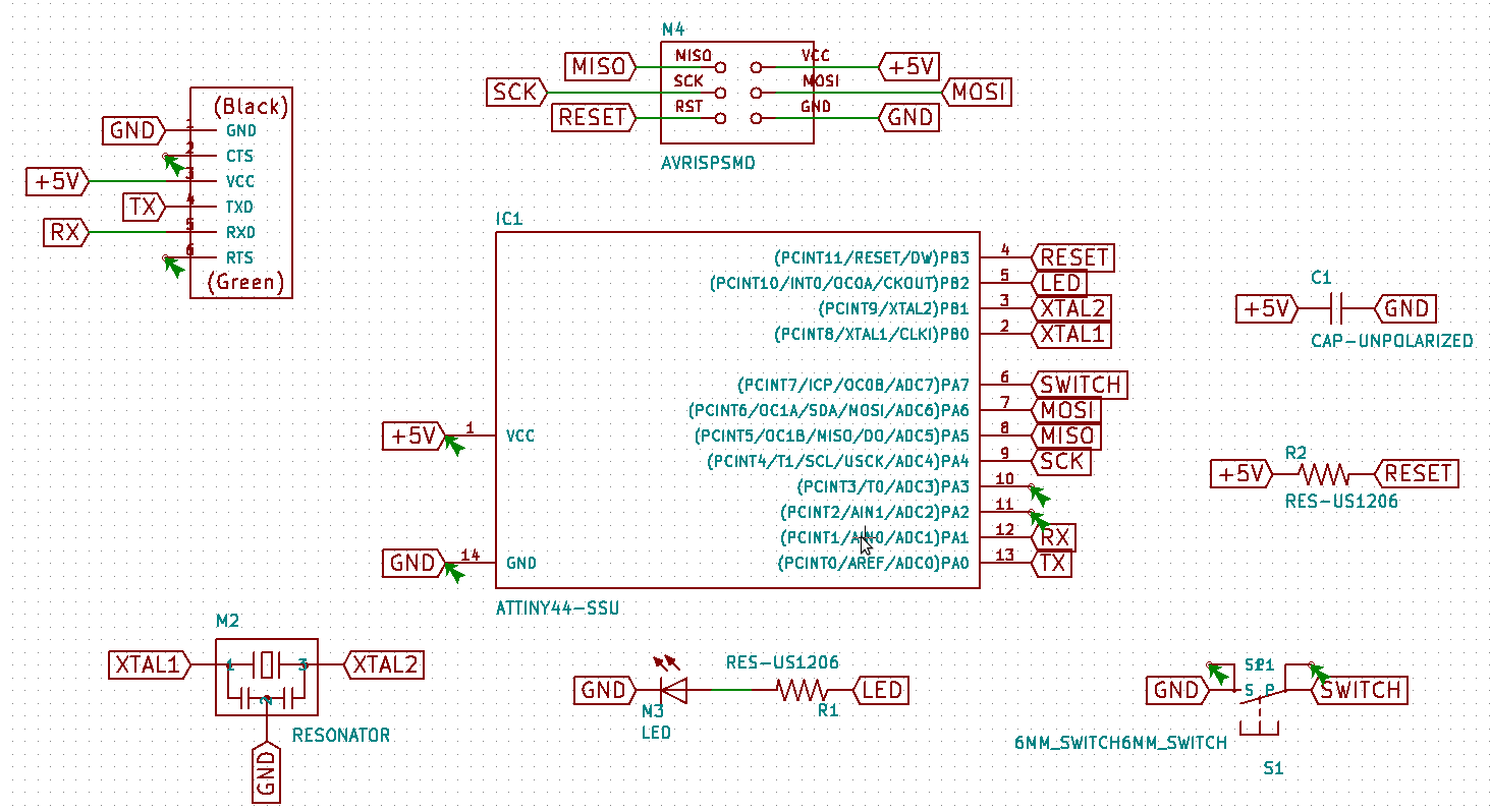
(...no relevant errors found...) / 2 -dialog
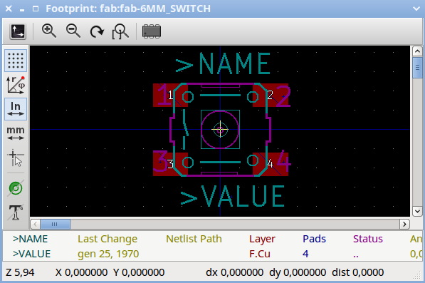
Next step is associating components with footprint through CvPCB tool
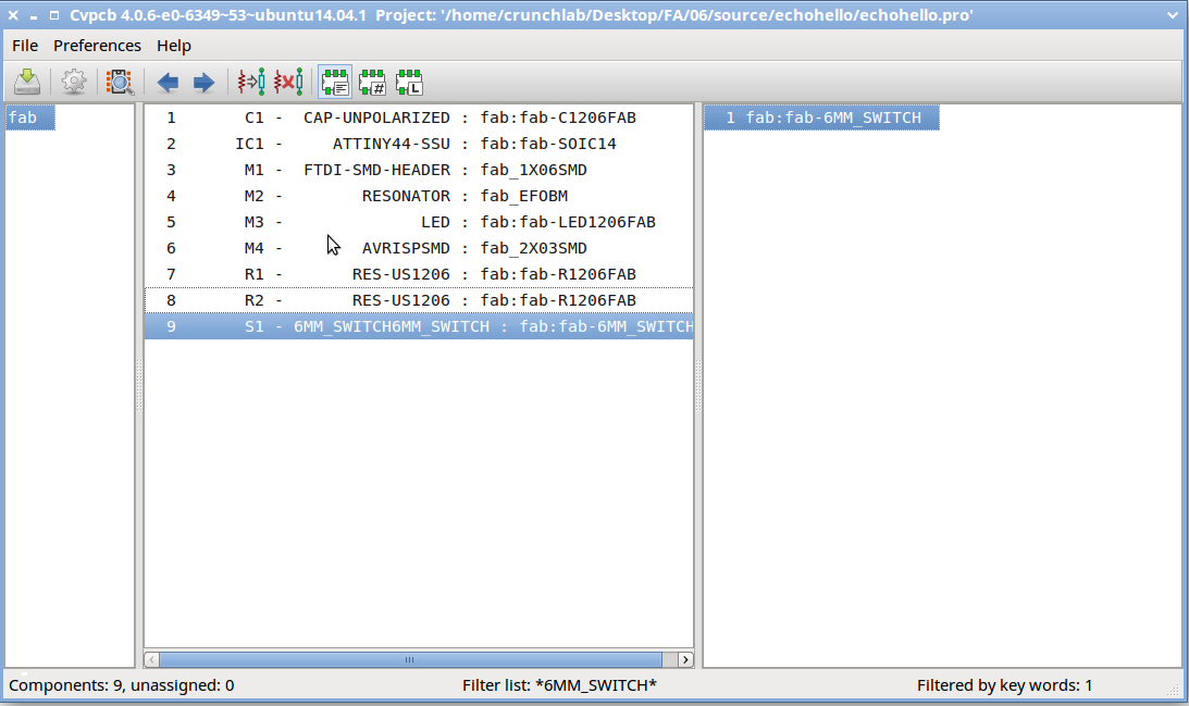
then exporting the "Netlist" to be then imported in PcbNew module
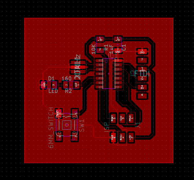
At this point components can be routed and rendered on the real PCB
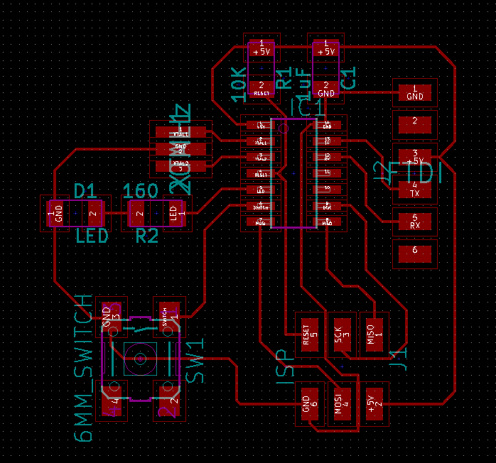
then prepared to export traces and edge cuts
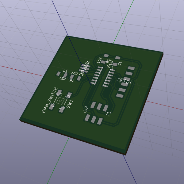
and rendered for visualization in a 3D image
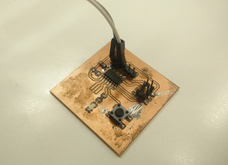
Here's the "Hero Shot" of the actual final echo-hello board result: milled, stuffed with components (for details see Week 04) and programmed with Neil's firmware, not before setting ATtiny84A-SSU microcontroller lfuse value to "0xE2" to make it working with internal clock
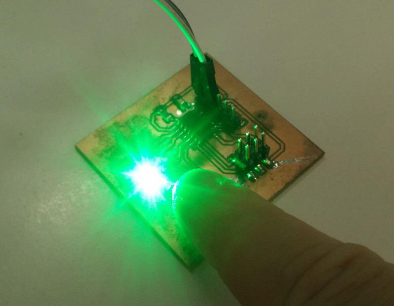
Testing it -working fine!
Source files
- hello.sch -KiCAD Eeschema output SCH File
- hello.net -KiCAD Eeschema output NET File (Netlist)
- hello.kicad_pcb -KiCAD PcbNew output KICAD_PCB File
- hello-F.Cu.svg -KiCAD PcbNew output SVG File (Traces)
- hello-F.Cu.png -Inkscape output PNG File (Traces)
- hello-F.Cu.rml -Fabmodules output RML File (Traces)
- hello-Edge.Cuts.svg -KiCAD PcbNew output SVG File (Edge)
- hello-Edge.Cuts.png -Inkscape output PNG File (Edge)
- hello-Edge.Cuts.rml -Fabmodules output RML File (Edge)