Electronics Production
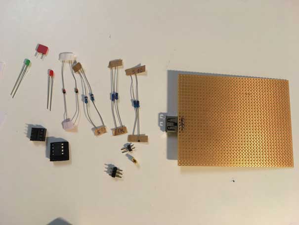
Soldering your own ISP is a quiet good way to get in touch with circuit boards. But before starting so I wanted to understand how this small programming board works. How is it wired and why some pins need resistors in advance and some not. I´d tried to understand the wiring in schematic files, and I draw a lot of small wiring plans of parts of it. For learning I took Zaerc`s FabTinyStar page And I think it was very helpful. Then I went to an electronic chain store: Conrad Electronics and bought all the elements I needed. I couldn´t get the same resistors like the one on the FabTinyStar page but similar ones. Anyway the resistors have a toleranz, so I hoped it would fit.My shopping List was as follows:
- 1x ATtiny 45
- 2x 1kΩ resistors
- 2x 510Ω resistors
- 2x 51Ω resistors
- 2x 3.3v zener diodes
- 1x red LED
- 1x green LED
- 1x 100nF capacitor
- 1x 2x3 pin header
- 1x USB female connector
- 1x perforated board
- 1x thin wires
- 1x tin-solder
- You also need a soldering iron and some holding, and enough light.
Learning about the board
I looked up in internet for the meanings of several pins and elements. I found out that SCK on pin 7 is importend for synchronisation given by master. Mos pin 5 : Master output Slave input; Miso pin 6: Master input Slave output; pin2 and pin3 are for data transfer. Furthermmore, I learned about zener Diodes: they are like a security mat, up til 3.3V nothing happens, but if the voltage gets higher they suddenly opens the passage to the ground. By the way GND is Ground and VCC is electr. supply. You have to take care how to intall them. They have are ringmark or black end or an arrow showing the direction opposite to GND. Alike, the red and green diode have a short leg showing the source. This has to be connected in direction to the ground.
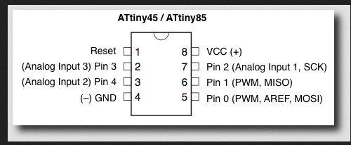
It is quite helpfull to know that there is a small dot in one corner showing the Reset pin1.
Drawings:
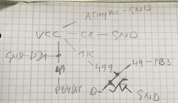
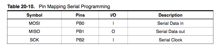
First, I´d analyzed all VCC connections I found on FabTinyStars schematic drawing.
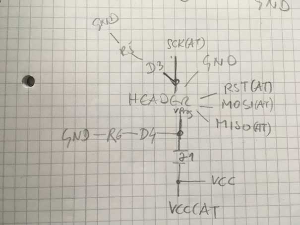
Then I analyzed the wiring from the perspective of the header.
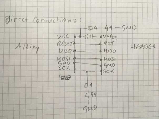
After that I recognized 4 direct connections without any branches. Miso/Mosi/Reset and GND. Miso and Mosi and Reset seemed ot me like the core of communication between header/.. and processor.
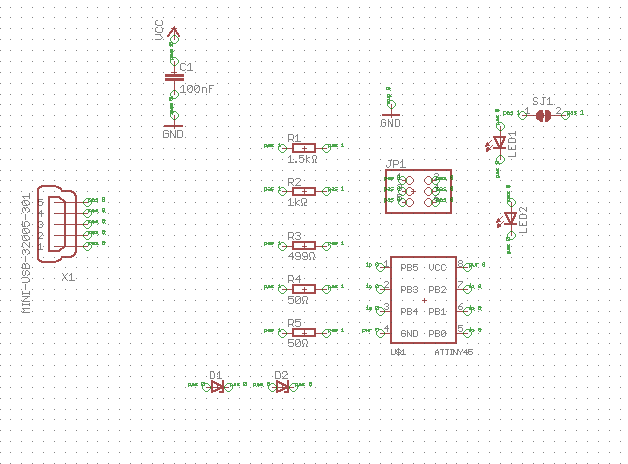
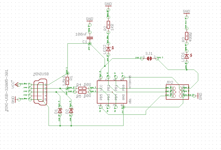
These drawings are just the final ones of a longer process of understanding. Below you will find the schematic drawing of the circuit board.
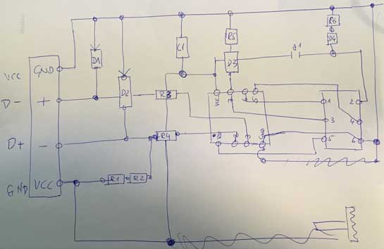
As you can see there is a turn-over entrance. The drawing was originally aimed for a male usb connector like the FabTinyStar, but then I desided to use a female one and had to cross. You will see later on.
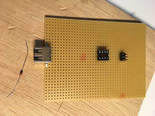
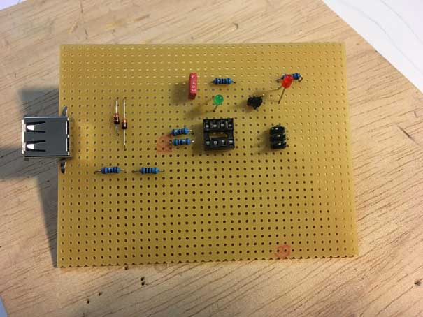
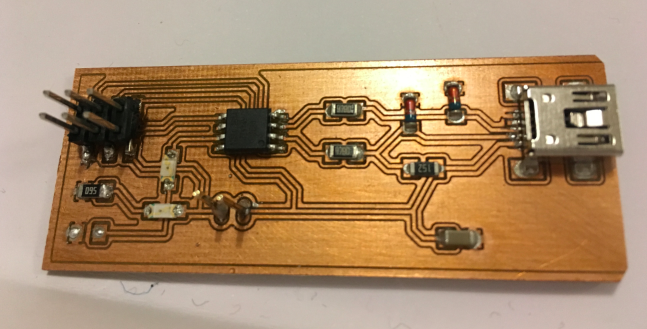
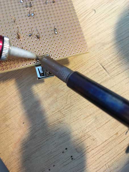
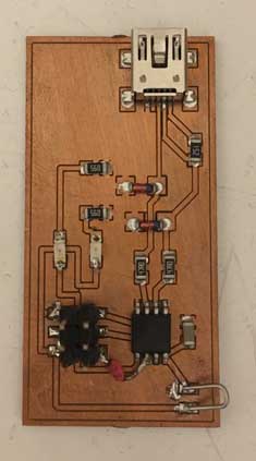
I started to solder the main parts first, sticking the legs through the holes and soldering them from backside. For ATtiny I desided to use an adaptor for not beeing too much afraid of soldering a processor.
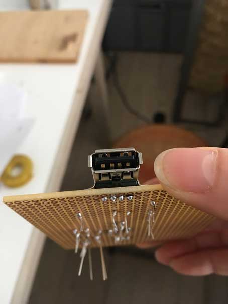
Now, I had to switch the connector from top to bottom to be able to use it in the right way shown in the above schematic drawing.
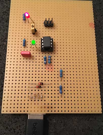
Here, you can see all parts solderd on the board.
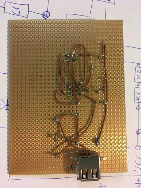
After soldering quiet a while I finished everything.
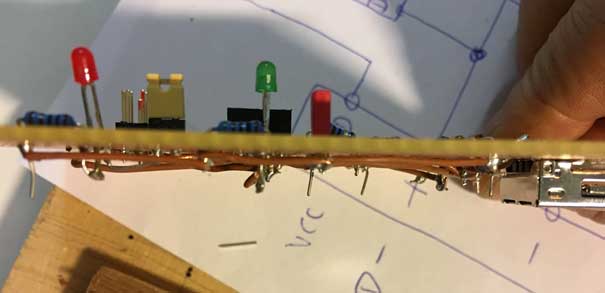
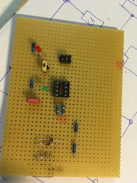
Function Test
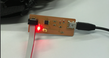
Finally, it was very interesting to see if the circuits will work, if the diodes will flash. It was a very fancywork and I had to look very accurate where to put my soldering iron. But relievingly it worked out:
My Eagle designed Board
designed with Eagle from Autodesk
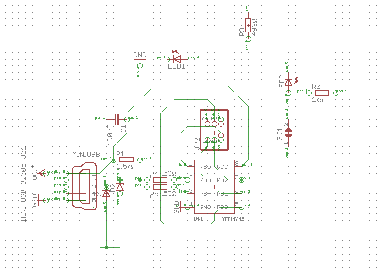
I took the wiring scheme I have drawn by myself (see above) and opend a new file in eagle: my personel pragrammer.I worked with Eagle 7.
A short introduction into Eagle:
I used the video tutorial created by 'Technical University Berlin'. For german speeking people I can recommend it highly.
Start Eagle and a control panel will pop up and amongst others you will find in this panel the library and projects folder. Eagle works a bit different from user interfaces. You click a tool e.g. Delete and afterwards you select objects you want to delete. In the library you will find components you need, I will explain this later. In the folder Projects you will find your schemes and board designs. But now, you create a new file. Do not close the panel. It will close the whole program. In Menue/File selekt new/scheme and an empty page with toolbars will appear. Now I will explain the most importent tools and workflow.
 Add from library. With this tool you pick all components you need to build a circuit scheme. With the add tool you can place as many elements e.g. resistors as you need and with esc-button on your keyboard you finish this command.
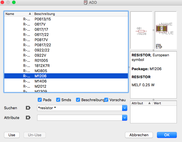 The library will pop up. You can look up in the list or write in search the name of the component if you don´t know the exact name you can write a partial name framed with *...*. After selecting your component the librariy window will close and the component will stick to your crosshairs. With left click on your mouse you place it.
After adding your components you can edit or move a component by clicking on or near its cross.
 Now, you can change the name of your component to be able to recognize it later on your board.
 With change value you can set the right value for each component, this is very important, because if you want to read your scheme years later or somebody else wants to read it and build it, you should know which components you used.
 If you need more then one component of one type e.g. resistors, then you don´t need to add all of them from library. You can just copy the first one and adabt the values and names.
 If any component or wire is wrong you select delete from toolbar and with clicking on wires or elements they vanish.
 Move is a very important tool, too. You select move, click on a component you want to move. It will stick immediatly to your cross hairs and you place it somewhere else. If it has the wrong direction, you can rotate it with the right click on your mouse or two fingers click on your trackpad.
 But you can also rotate with the rotate tool.
 First you have to select the command you want to do e.g. Delete. Afterwards, you select group tool and draw a frame around a set of elements you want to delete. They will change their colour and with the right click on your mouse you can choose delete: group. To finsh the command delete you press esc.
 Before you start to wire them click on grid to set the grid dimensions. I like to use mm and first I took the preset size 2.5 mm.
Later on in board file, I switched to finest grid to be able to wire them more accurate.
Before you start to wire them click on grid to set the grid dimensions. I like to use mm and first I took the preset size 2.5 mm.
Later on in board file, I switched to finest grid to be able to wire them more accurate. With layer you can make layers visible or invisible.
  With Net tool you can wire all components.In the above command line beside the grid icon you will see all designs of wiring.
 After wiring it is possible that you can´t read the names and values of your component anymore, too many overlapping labels. With smash you can uncouple them from the components and set them in a readable way.
  But you can also make the informations about values and names invisible see them only with the icon Show. With this icon you get all informations about this element.
 Now, switch to board layout. You will find this icon in the above command line where the magnifiers are.
All elements will be set beside your outlined platform with the wirings . You have to drag them inside this outline. Keep your scheme open to be able to check the wiring. I didn´t use autoroute you will find at the bottom of the toolbar. I set all wirings by my own, it took a while. Again, you place all components with the icon move. And start routing on top layer with red lines on bottom layer with blue lines. You can see all layers by clicking on layer icon.
 With Ratsnest you set automatically the shortes ways between the conected components. It is helpfull to do it frequently to organise the board.
  Routing demands a carefull settling to receive a connection between two components. It is easy to recognize if it didn´t work out, the routing line doesn´t stop to route, furthermore it sticks to your curser. Also you will hear a sound when routing works out. For this part of work it is good to adjust the grid.
You can´t delete the red lines anymore you just can change them into bee lines again through clicking the Ripup icon.
Routing demands a carefull settling to receive a connection between two components. It is easy to recognize if it didn´t work out, the routing line doesn´t stop to route, furthermore it sticks to your curser. Also you will hear a sound when routing works out. For this part of work it is good to adjust the grid.
You can´t delete the red lines anymore you just can change them into bee lines again through clicking the Ripup icon. If you click on change tool in the toolbar you will get a list of possibilities like diameters, Font, Layers..
 Finally, you should do an electrical wiring check.
 Finally, you build a polygon around your board, to be able to use your board as GND. In the top symbolbar you can choose the width of your polygon, if it as filled up, hatched or cut out and you can choose Isolation size of your vias. Click again on Ratsnest and you will see that the board will filled up with red colour.
 After finishing the board design you can send it to LPKFCircuit Pro for milling. Choose Cam icon in the top Symbolline. A window will pop up and asks for executing the job. Select in Menue/File/Open/Job/LPKF_Export.CAM. Then click Execute Job. LPKF Circuit Pro is a milling software for our LPKF millin machine. Now, you can follow the above instructions.
My Scheme Design
start adding
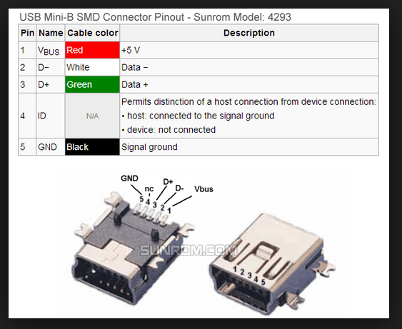
After adding the sign for mini-usb I was a bit unsure about the orientation. I looked up for mor information as in the following screenshot:
start wiring
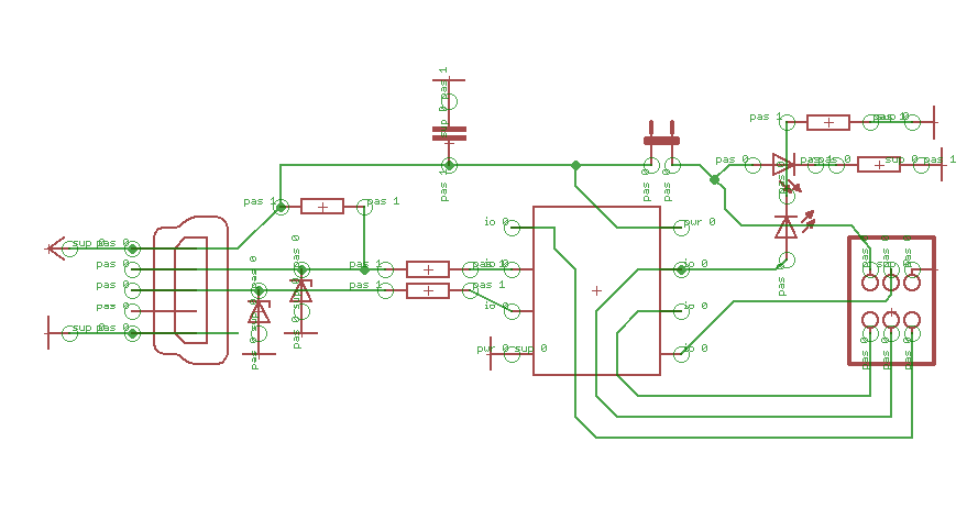
scheme changes
more scheme changes
spiral connection
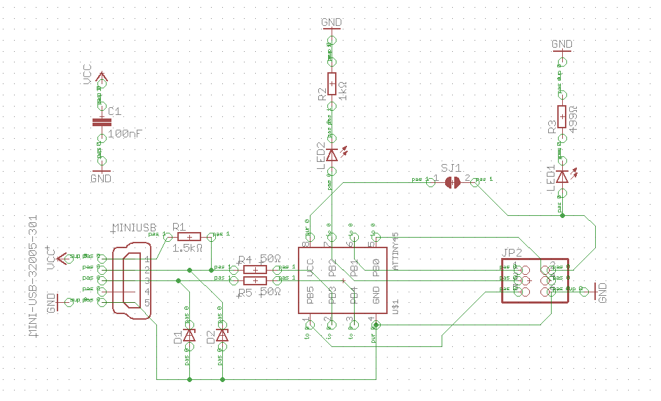
finished scheme
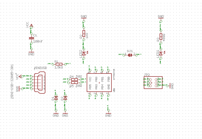
My Board Design
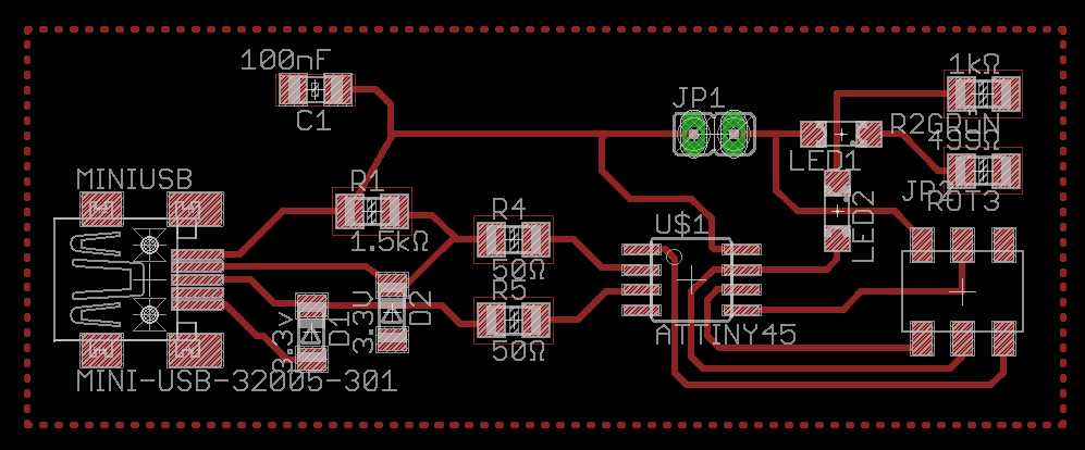
board before rastnest
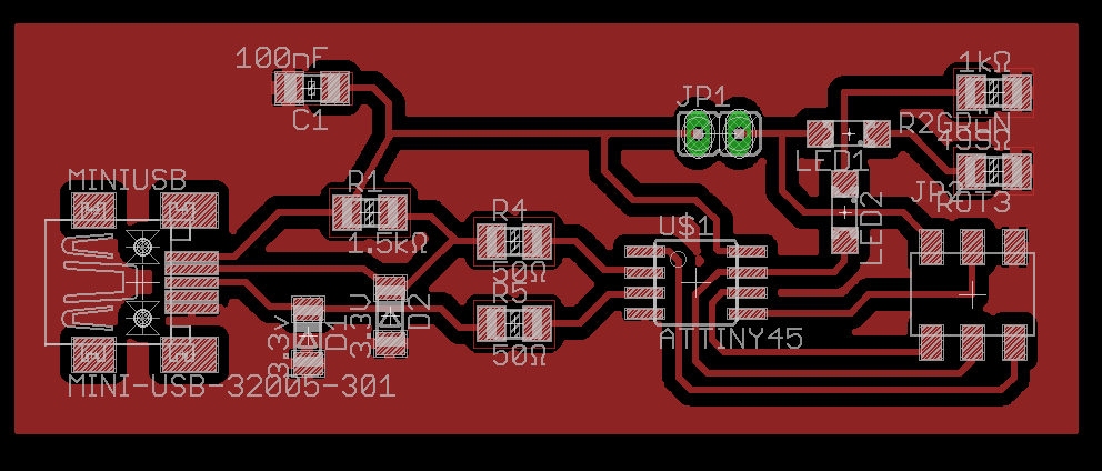
board after rastnest
Both files for download:
Aleks' Programmer Scheme
Aleks' Programmer Board
Milling a circuit board
After soldering my own board, we got the chance to mill one. As I had to decide, either drawing a board in Eagle with no understanding how it works or analyzing first I didn´t finish my eagle design board. Marcel offered me to mill his design for our milling exercise. Thanks a lot, Marcel. The following part is about cnc-milling with LPKF Laser and Electronics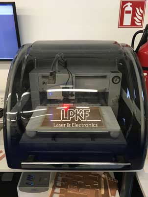
First of all turn on the machine and your connected computer.
 Start Eagle und open your file under CAM/Job/Export LPKF-File.
Select Process Job.
 Start Circuit Pro (milling program) ,
click The way of processing and choose under File/Templates the Single Sided Top.
 Then choose Prozess Planning Assistent and select Edit Circuit Board:
Choose:
1.One-Sided Top2. Substrate: FR4/FR5
3.click : ready
 Choose: Datas from Free Format and select all Files with Upper Case endings
click Open. The board will load.
Optional: if you want to mill both sides you can set center holes with Fiducials.
 Choose: Cutting Generator and
select: Isolation Method: Single, Pads double
Choose: Cutting Generator and
select: Isolation Method: Single, Pads double  and choose your desired contour.
  and look for the milling depth: e.g. 18µm
Start and Close.
 Choose: Circuit Board Fabrication Assistant if all settings are correct press Start
Choose: Material Setting check the settings and press Proceed. Then, the window for Positioning will pop up.
 Select: Positioning by Mouse Control and after clicking in an area where you want to mill your board you deselect Mouse Positioning and drag your board to this position. If you select MP again you can verify remaining edges of the board. Don´t forget to deselect afterwards.
Save as *cbf
Select: Positioning by Mouse Control and after clicking in an area where you want to mill your board you deselect Mouse Positioning and drag your board to this position. If you select MP again you can verify remaining edges of the board. Don´t forget to deselect afterwards.
Save as *cbfAfter saving machine starts by itself.
Milling Process:
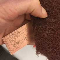
- emergency stop: For preventing a crash just open the lid, the machine will stop immediately showing -Error- you have to remove again. We used a 0,2mm moulding cutter by 18µm cutting depth. After milling finish and close the program. It will ask, if the milling head has to go back in rest position: just affirm Allways vacuum the table afterwards. Check the board under microscope:
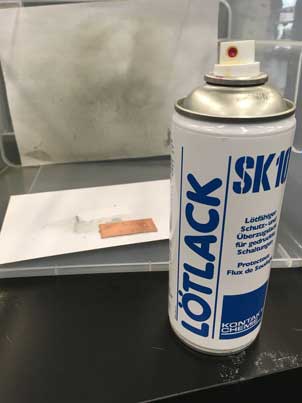
Sand and varnish your board
Assembly with insertion machine
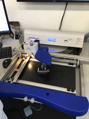
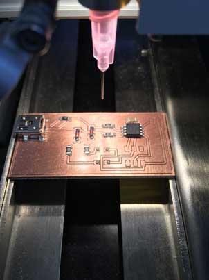
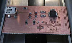
It is better to assemble very small components with the help of an insertion machine, like the one we have: ProtoPlaceS - Manual Pick and Place Turntable . Using a mountable injection first you put some soldering paste on every spot you want to solder with an element.
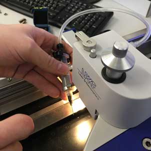
For bigger spots you can place a bigger drop for very thin spots a smaller drop. It is very helpful to regulate the amount of paste by the control keys. For bigger spots 0,5 sec for tiny spots 0,3 sec. You just press the foot pedal and wait till it stops. Always clean the needle with blast you finished your work. For placing the components you need to dismount the injection and use air draft needle to pick them up and place them. Every time you tip a component air draft will start or stop.
Soldering furnace
For soldering the components on the board, the board assembly can be heated up in the soldering furnace until the soldering paste turns into clear silver colored tin-solder.
Preheat temperature 170° Celsius Reflow temperaturs 250° Celsius Cool down Take out the board and solder the header and all LED left over . Solder the Jumper.
Problem with programming
After finishing the board we found out that some tracks were missing and hat to solder some additional wires. But still programming didn´t work out. Tobias, our Instructor,inquired problem we all had and finally he got it: the resistence connecting to the serial clock wire disturbs the connection during programming. So we hadt to unsolder this resistence with intent to solder it later, again. Meanwhile I decided to design my own board.Also, Marcel redesigned his board.
Programming my Programmer
After soldering all elements onto the board,I closed the Jumper with a removeble bridge and opened Brian's programming tutorial and with Tobias' back up I started programming as follows:
- Download and install CrossPack AVR. CrossPack AVR is a Toolchain for Mac mainly for programming Atmel's AVR microcontrollers. You will not find a software icon in Applications, because it is running background. You can test if you have installed CrossPack by writing avrdude in your terminal. Then you will get at least a response telling you avrdude' e.g. version number
- In Terminal Change directory (cd). Go into Downloads, where your downloaded Crosspack and look for fts_firmware_bdm_v1. Change directory again into fts_firmware_bdm_v1 and writemake. Make is not only limited on beeing a compiler. You can use make following by a target like prog: Create a file named prog. Using make without any argument it will try to create a workable program. You just write make and it will create fts_firmware.hexfile. If something went wrong consult the errow messages for more information about debugging.You can check the existence of the hex-file by writing ls in your fts_firmware_bdm_v1folder and look for it in the list.
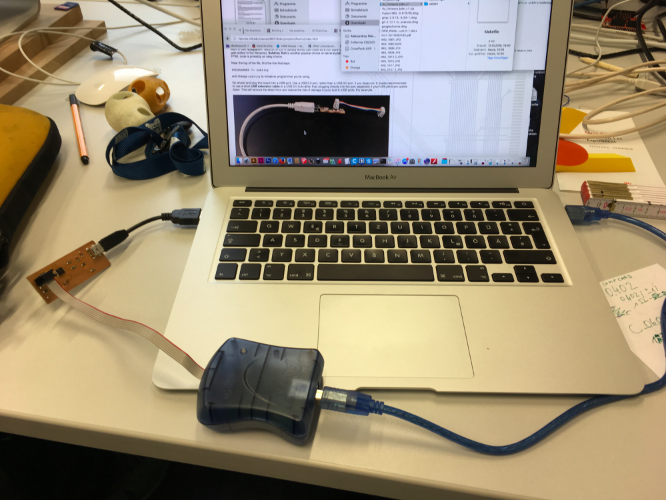
- Now, plug your board into an USB port, via USB extension cable. Take care which type of USB you are using: mini-USB (B) or normal (A)? Your red LED should light up.If not check jumper if it is brighed. If something wrong with the USB device check unplug your board and check for shorts.
- After your board is checked connect the programmer via your soldered ISP header between your board and your computer. You get a circuit. For connecting programmer and board you use a ribbon cable with special connector your have to take care about orientation: The cable or connector has a sign for marking Pin 1 the Miso line, place this onto the header in same orientation: Pin 1 Miso line. (See also ATtiny pin content above)
- Afterwards write make flash in Terminal. It will erase the target chip and program its own flah memory with contents of .hex file you allready created in yourfts_firmware_bdm_v1folder. You will recognizing the programming process though the following command line:
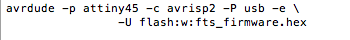
This above command line shows the prgramming command avrdude in dependence of your attiny45, avrisp2 and usb. In this dependence it will program your hex-file new. You will see the workflow: Reading, Writing, Reading and Verifying and Avrdude Done. If something went wrong you have to check all connections again, be sure their are no shortcuts. - Now it is time to set the configuration fuses with make fuses.It will set up all fuses exept the one for reset pin. You will see again a process with reading, writing,veryfying.If something went wrong but the above step was o.k. then you have definitly an intermittence somewhere.
- Before disabling your reset pin fuse to be able to program with your programmer it is recommendable to test the usb functionality. Unplug your board from your computer and disconnect the programmer completely. Plug your board again into your computer.Click on the Apple symbol above in the left corner, then About this Mac, in General (Uebrsicht) you will find below the Report (Systembericht) button. Click on this and if everthing went well you will find under Hardware/USB your connected ISP: USBtinyISP.
- At least, blow the Reset Fuse. Write make rstdisbl when your ISP programmer is one more time connected to your board (make a circuit again). It is the same workflow like bevore with the difference that your fuse on reset pin will be disabled. This command will turn your reset pin into a GPIO pin. From this point you can not reprogram your ATtiny45 anymore.
- Remove the bridge from jumper to disconnect Vcc form Vprog pin.