Week6 : Electronic design
This was the first time I used Eagle software so I started with the tutorial forby Anna Kaziunas I used the version of Eagle before it was incorporated into Autodesk packages. I started with the helloEcho circuit file as a base and started adding my components.
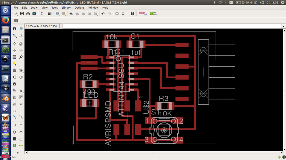
Circuit Schematic view
But before that I had to install all the necessary component library, I added both the ng.lbr and fab.lbr. So first start is the schematic which I found to be very intuative, simply to add components I click on the add icon just right to the trash can icon. The menu to select from is on the left of the schematic window and by hovering on any icon the describtion will appear on the lower left corener of the screen. I first tried to explore what each icon do by chosing it and trying to do some changes.
I added first one LED from the ng.lbr keeping in mind those remarks in Anna's tutorial.
(always choose the 1206 components) (these are the ones that have 12mm x 6mm packages)
Placed it in an empty space on the workspace and clicked then pressed ESC button. Where it took me back to the componenets list, so then I added a resistor and a OMRON switch. At this point I had my compoenets lying down on the schematic workspace not connected. I just didn't start connecting them yet.
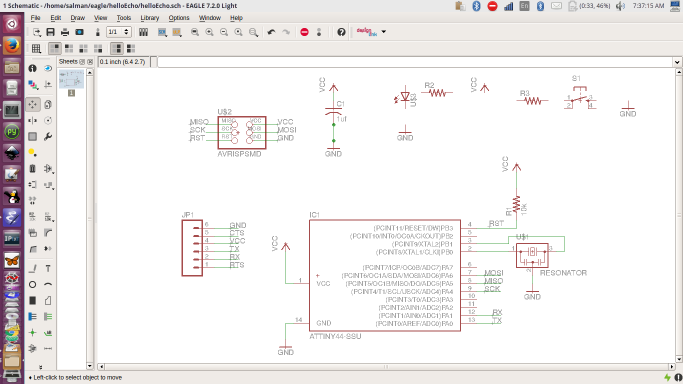
Then I statred connecting the wire, I chose the right angle bend style for the wire. Again wiring is simply clicking while selecting the wiring tool between the points. Now I have a single LED and a Button in the Schematic, with both a current limiting resistor and a pull up resistor respectively.
Resistors function
F the necessary value for the resistor i need to add. Which can be calculated by the following formula :
R = ( Vs - V led ) / I led

Voltahge Source (Vs)
Voltage forward voltage (V led) 2.2 typ. 2.6 max V from DataSheet
Current through the LED (I led) 20mA from DataSheet
Resistance (R) this is the value we are looking for
the current limiting resistor value needed is 120-140 Ohm or greater.
The calculation is also explained in the illustration below.
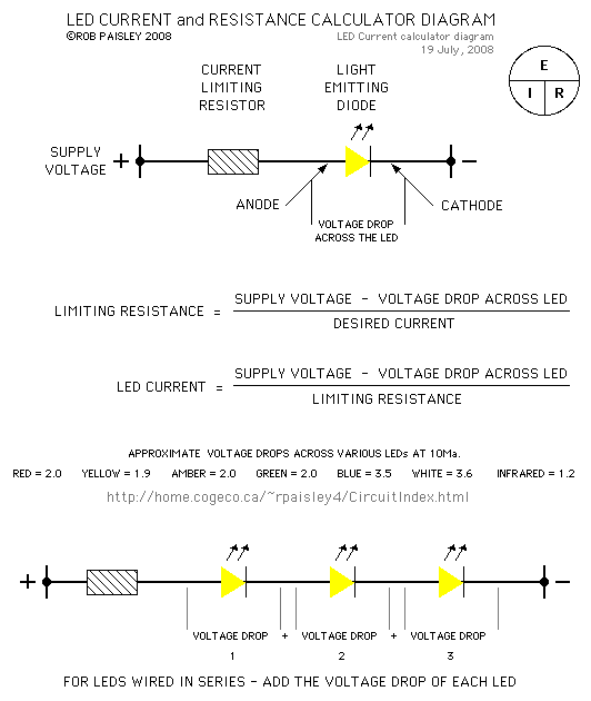
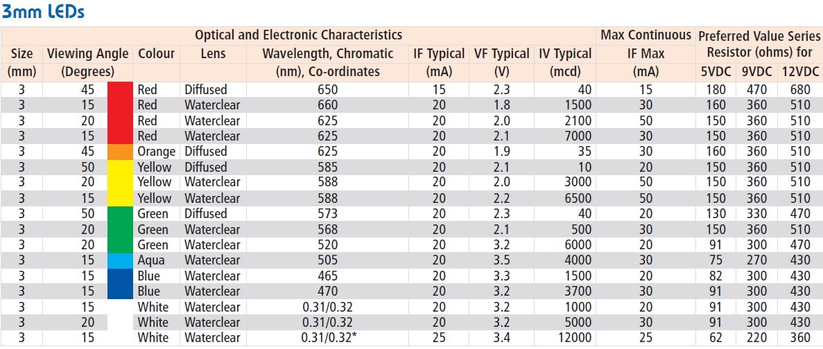
While the current limitng is meant to protect the LED from damage by a higer current as the name implies. According to the LED DATASHEET there is two forward voltages a typical forward voltage and a maximum forward volatge. I did my calculation based on both those value. For the Max it's 120 Omh and The typ. it's 140. In The following table a guide to different 3mm LED, it is also relevent as I noticed to values of the OMRON LED I used.
The external pull up on the other hand resistor is used to prevent floating or unknown state ( is the pin pulled high if connected to VCC or low as if connected to ground) this specially if the button is closed. The resistor when the button is not connected allows a small amount of current to run between vcc and the pin hence pull up. while if the button is connected it will prevent the flow of current between vcc and ground (short).
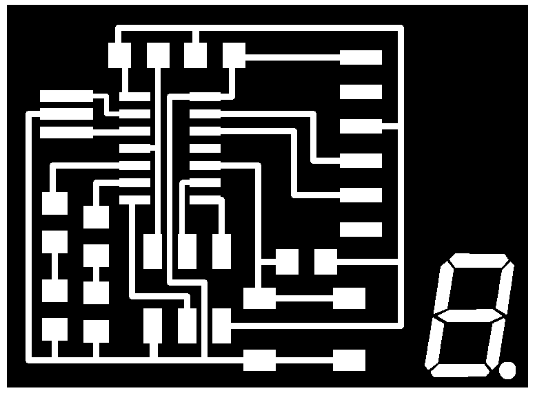
In the schematic adding name tags to wire ends and pins on the microcontroller will result in having traces connecing those ends in the Board layout. Then one has to do routing of those connections to get to something like the following. First step is to add a label to the end of the wire and microcontroller pin. And makin sure they are both named the same.
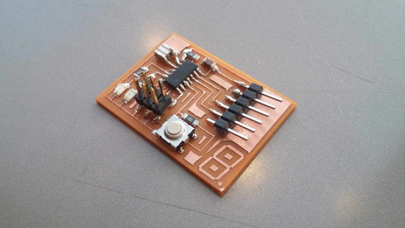
The Board View
Then on the board window I had to position the LED, resistors and button within the boundaries of the circuit rectagle. Wich i had to exband to accomodate for all the components added. Then using the route icon I would run over the thin traces to create the final traces. After that I used the moving tool to move traces around to have a uiform shape.
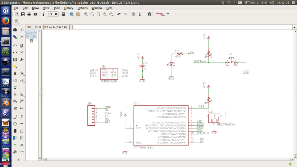
Then I added another LED. In the following image the traces prior to routing are shown for the new LED and resistor.
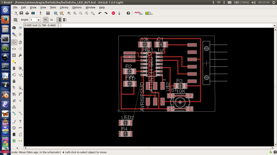
Followed the same steps as previuosly mentioned when adding first LED, but I had to do more adjustments. I had to rotate some components and align them vertically to have some space.
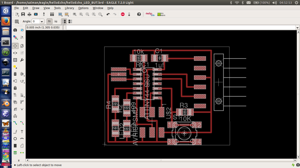
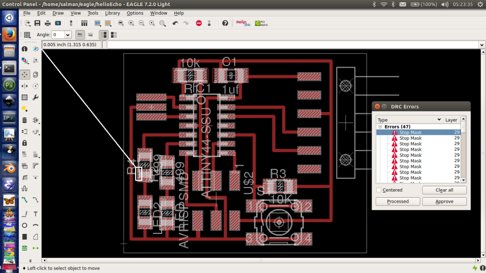
I didn't face any problems designing, but when I tried auto routing or circuit analysis then I realized that how little I knew, I started getting may errors related to mismatch between pads size and components.
Exporting Traces
Before exporting the traces to a photo editing software, I had to hide all unwanted layers. So in the view menu I selected Layer setting then I chose none to deselect all, and I just chose the top layer in the Board view from the layers pull down menu. Then in the File menu I chose export->image. I changed the resolution to 500dpi, and ticked the monochromic box.
The Image Editing
I opended the exported png file from previouse step in GIMP and added modified the canvas size by adding 20px boarder all around the canvas. make sure the width and height are linked and to press center before pressing resize. I added our Fab Lab logo to the right corner and then i flattened the image and saved it as my traces.png.

Then I filled with a bucket-fill the traces with black color and only left the white borders. I exported this image as the interior.
Milling the Board
Placing the stock on the Milling Bed
Switched on the milling machine I pressed the view button to bring the bed forward. Unscrewed the bed from the machine I fixed the copper on the milling bed with double sided sticky tabe and screwed it back. And I fixed the 1/64 milling bit.
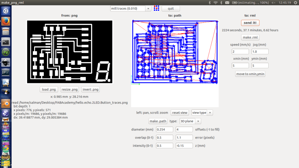
Starting Fab Modules
I used Fab Modules to mill the board, i used the png to .rml.process so I started with loading the png file.Chose mill traces and Chose 2 as the speed and set the Z min to -0.15. Then used the jog, I changed the values of X and Y just to jog it slightly away from the edge of the pcb board. I used 5 for both the X and y.And pressed move to xmin ymin.
Zeroing the Z axis
I zeroed my Z axis by manually lowering the mill ( pressing arrow down on the milling machine buttons) then I lossened the lock on the milling bit to have it tip just touching the copper and then I tightened the lock again.
Creating the GCode and sending it
Pressed make .rml and then send it and when I got to the next window I started milling.
Milling the interior
When milling was done for the traces I pressed view button on the milling machine changes the bit to 1/32 tightened the screw on the drill bit then lowered it manually again using the down arrow, open the lock screw and made sure it touches the copper board. Then locked the screw again and made sure to use the same X min and Y min as previously to be 5.After loading the interior png I Chose the relevant milling option and pressed again make .rml and sent it. And started milling.
There is a hack that I learned which i guess is not safe but without it zeroing the Z axis is not so easy, The plastic cover of the MDX15 has a safty metal piece that would cause the machine to halt and change to view mode once the front cover is opened. I had to unscrew this metal safty piece from the plastic cover and keep it in place in order to get the manual process of zeroing the z axis done without interuption.
The milling was uneventfull, luckly this was a fresh drill bit that I just got. I tried to time myself and keep things within a target time, if I removed all the interuptions i had between the stuffing and milling the circuit the whole assignment took just slightly over 8 hours to design, mill, stuff and program ( With Arduino IDE).
I also managed to sulvaged the Attiny 44 from another isbtiny circuit that had failed in week4. Using a heat reflow I went over the soldered pads of the attiny several time while holding it with a tweezer and after several runs with the heat gun the attiny was easly removed.
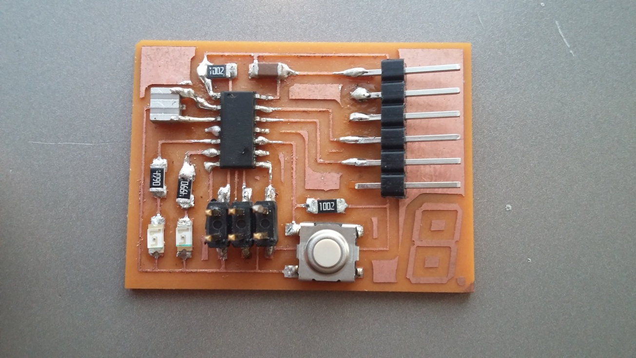
I did incorporate two LEDs and a button to be able to test different programs later. The first idea was to have the button switch between the two LEDs when pressed.
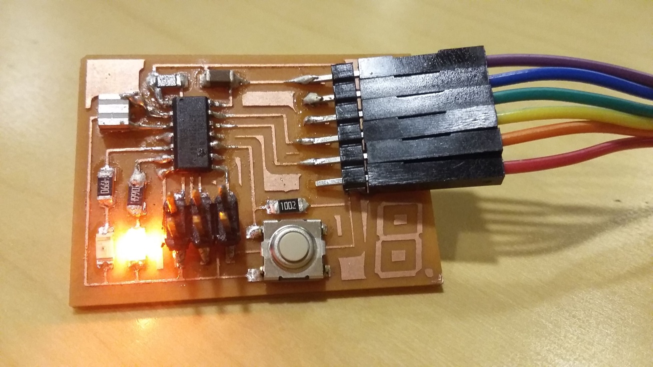
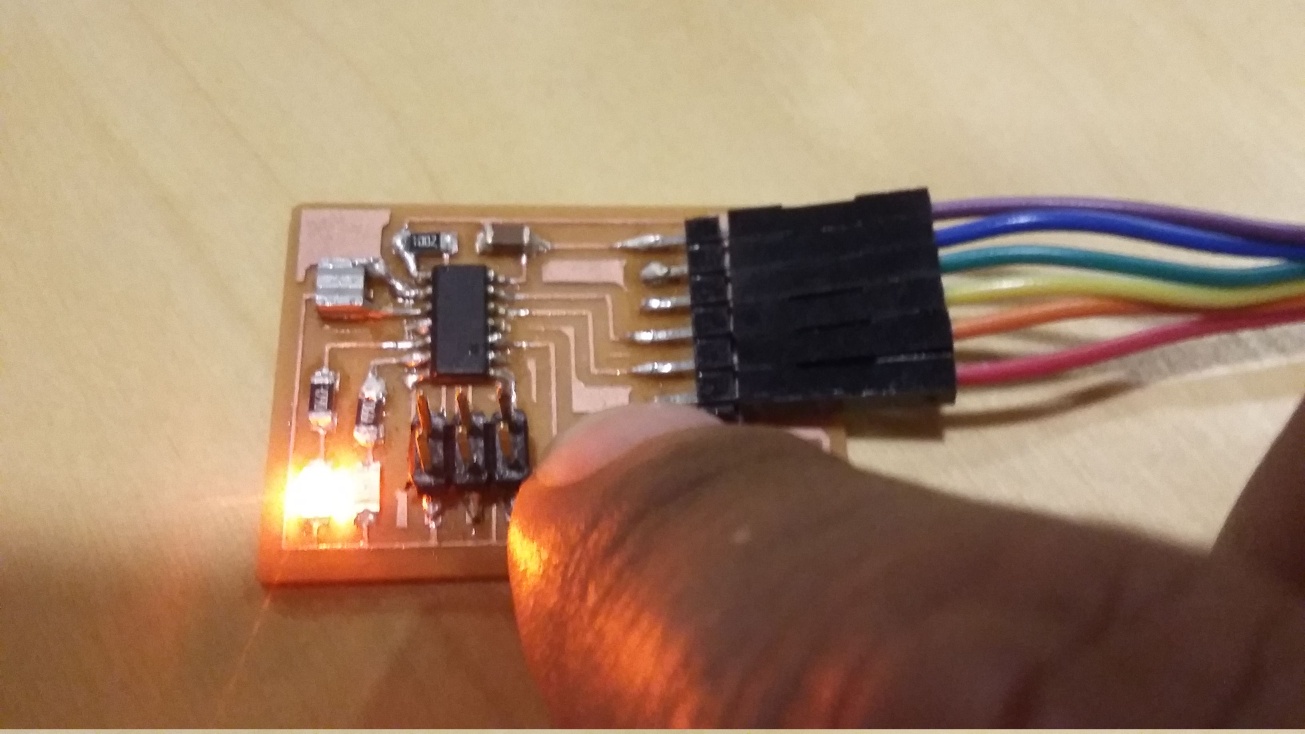
The program was a modification of the a button sample script, I used Arduino IDE to write the program, but usbtiny as my programmer.