2016
Electronics Production Mar 2. 2016
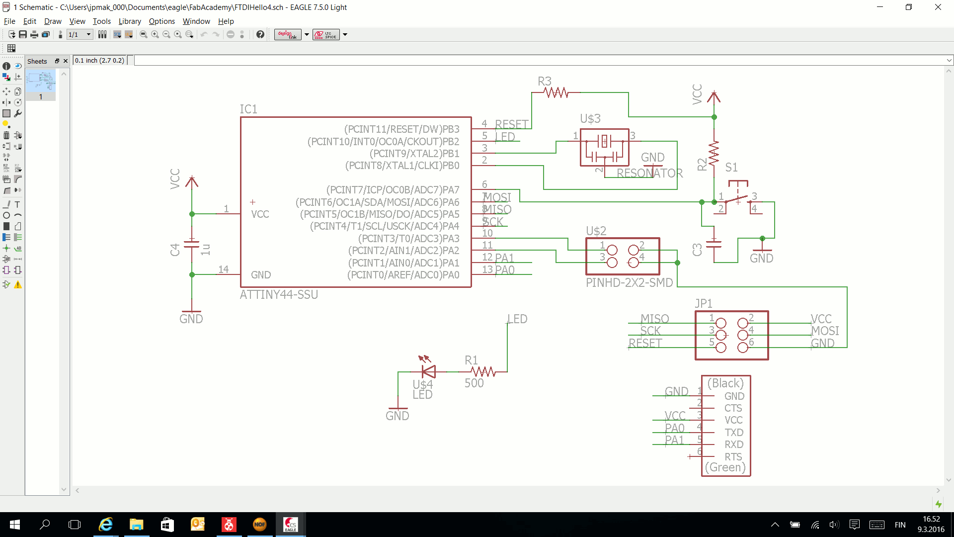
This week we continued with printed circuit board design and fabrication. The assignment was to reproduce echo hello-world board with additional LED and push button.
I started the work by downloading the latest version of Cadsoft Eagle and installing the fab.lib components library. These components are in the Fab Lab inventory and therefore readily available for later designs as well.
Create new project-Right click on the created project and create new schematic. Adding the components from the fab library is straight forward process.
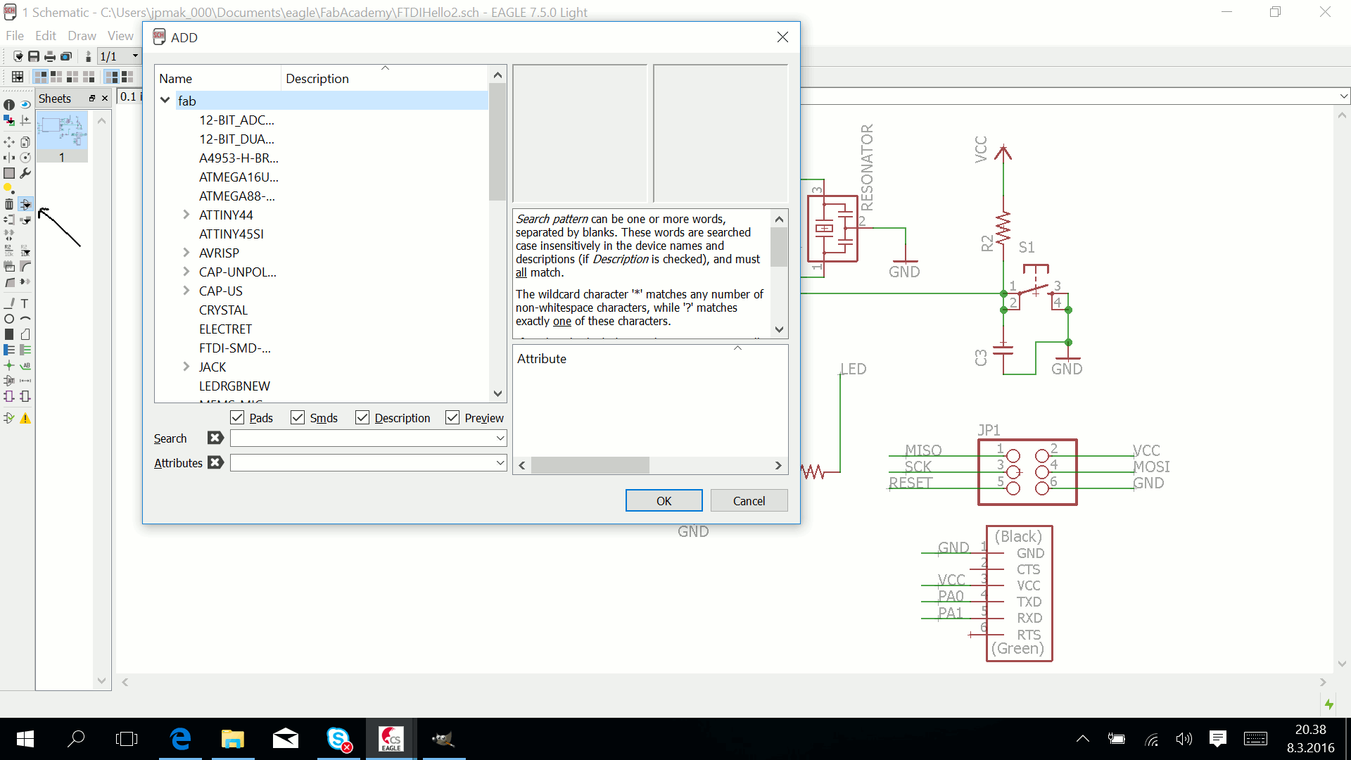
Once the components are placed on the schematic, we can start to connect them by using the Net tool. Do Not Use Wire tool. It has much less automated functionality. The wire tool can be used for drawing outline in the board view later etc.
If the wiring becomes too crowded, you can use name tool to label the wires and connect them that way. Similarly named wires are connected in the board layout.
Once the layout is ready, switch to the board view (File-switch to board). If the background is white, you can switch it black from Options-User interface.

Next, we need to design the wiring on the board. First, you need to place the components inside the defined board area. Otherwise the free version of Eagle won’t let you do the wire traces. After this, I used Autoroute. First, I selected the bottom layer as N/A to make only one-sided board.

First attempt of Autoroute was not successful. There were several un-routed connections as seen in the picture bellow.

After several trials of moving and rotating the the components as well as increasing the board size I managed to autoroute a board with only one missing connection.
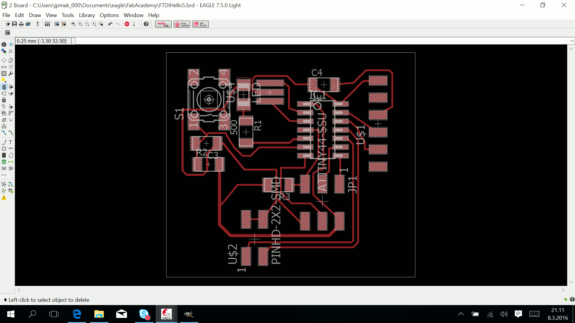
That was easy to connect by hand by using Route tool.
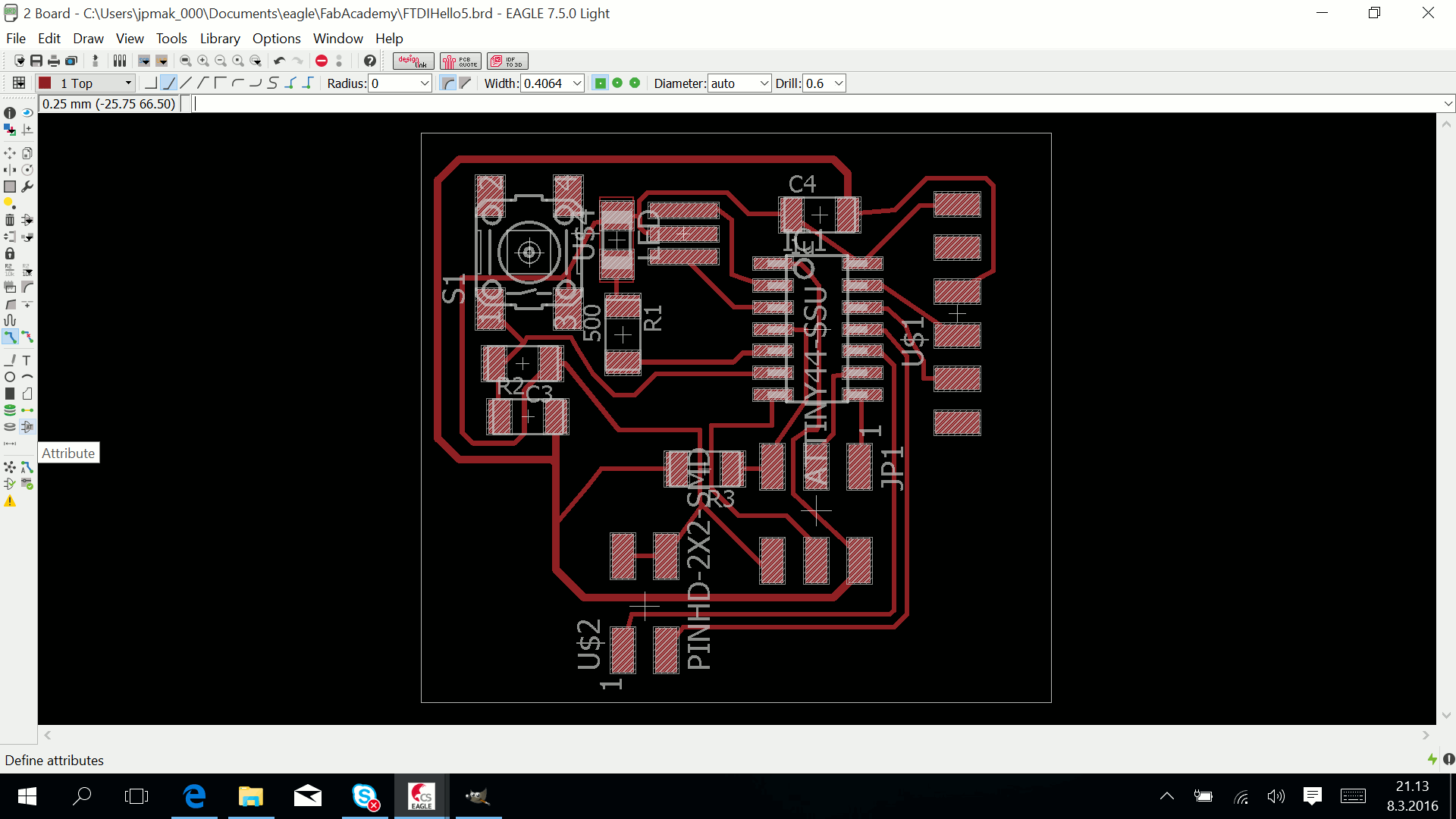
After that, I did the DRC check by using the values shown bellow. That way it is possible to mill the board with Fab Lab bits.
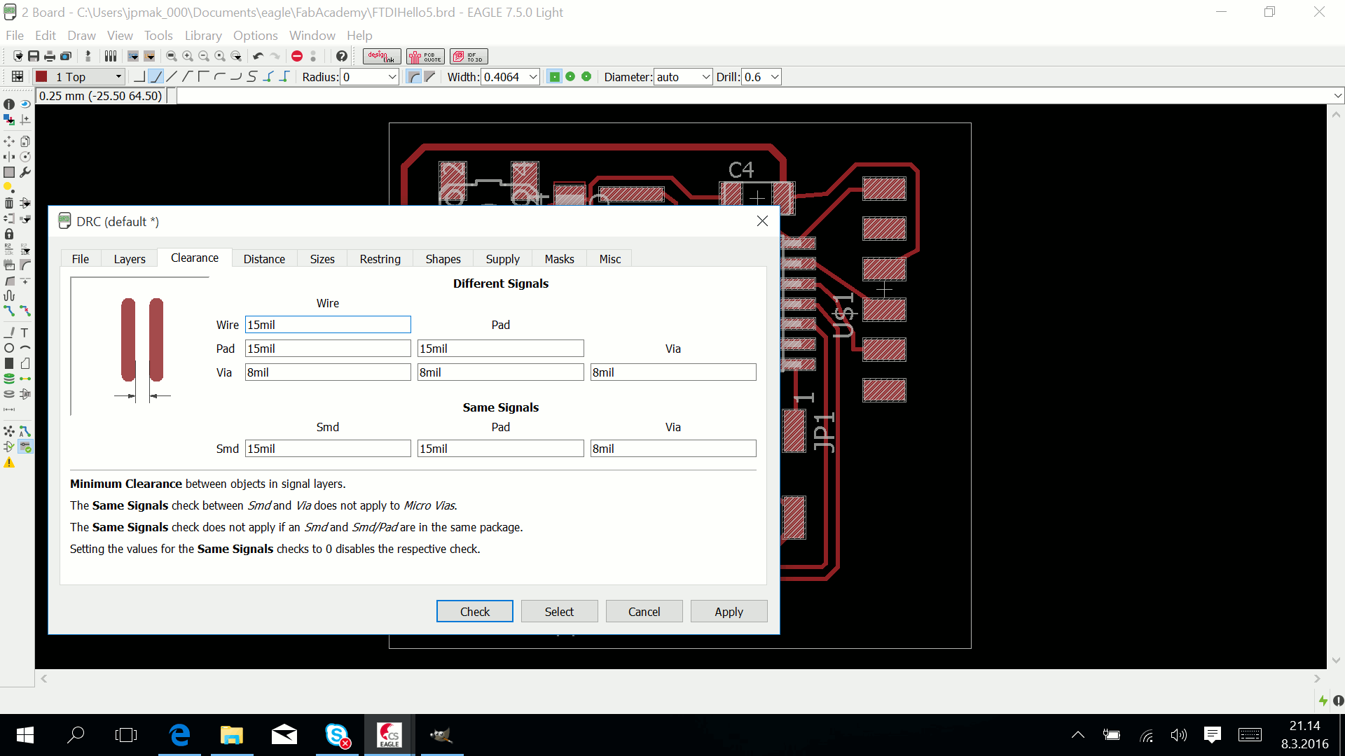
If there are errors in DRC, the origin of the error can be detected by clicking the error line.

Next we can do so called copper pour, which can increase our ground plane as well as speed up the milling time since we do not have to clean the board from copper but do only isolation milling. This is done by drawing a polygon around the board and pressing Ratsnest button.
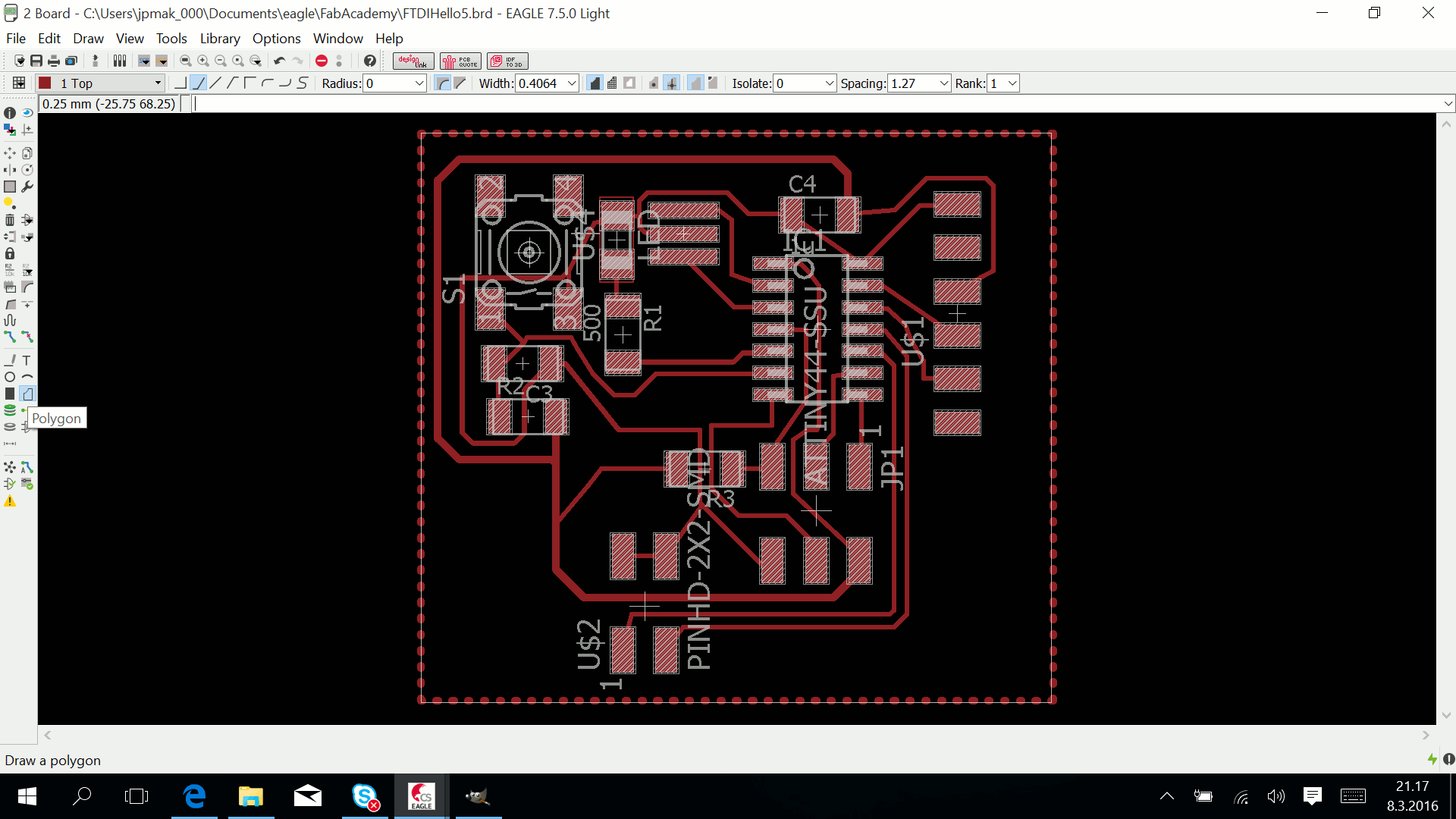

In order to make the board a bit more milling friendly, we can increase the clearance between the traces and copper by selecting the wrench tool and adjusting the isolation parameter.

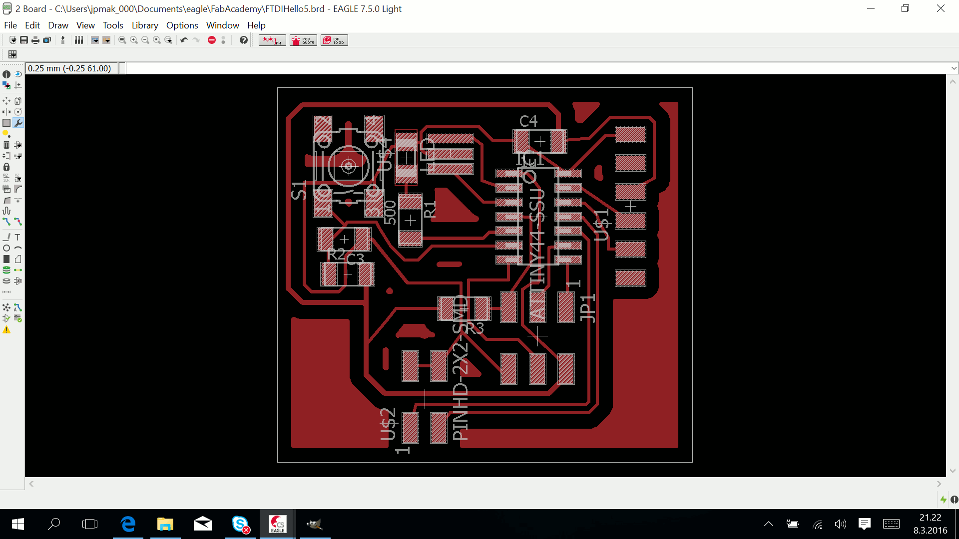
The final step is to make the board export ready. We need to remove all the not needed graphical elements by selecting View-Layer settings. We only want to have Top and Outline visible. Then we use File - Export - Image command to save the board as monochrome png file. Resolution should be more than 1200.
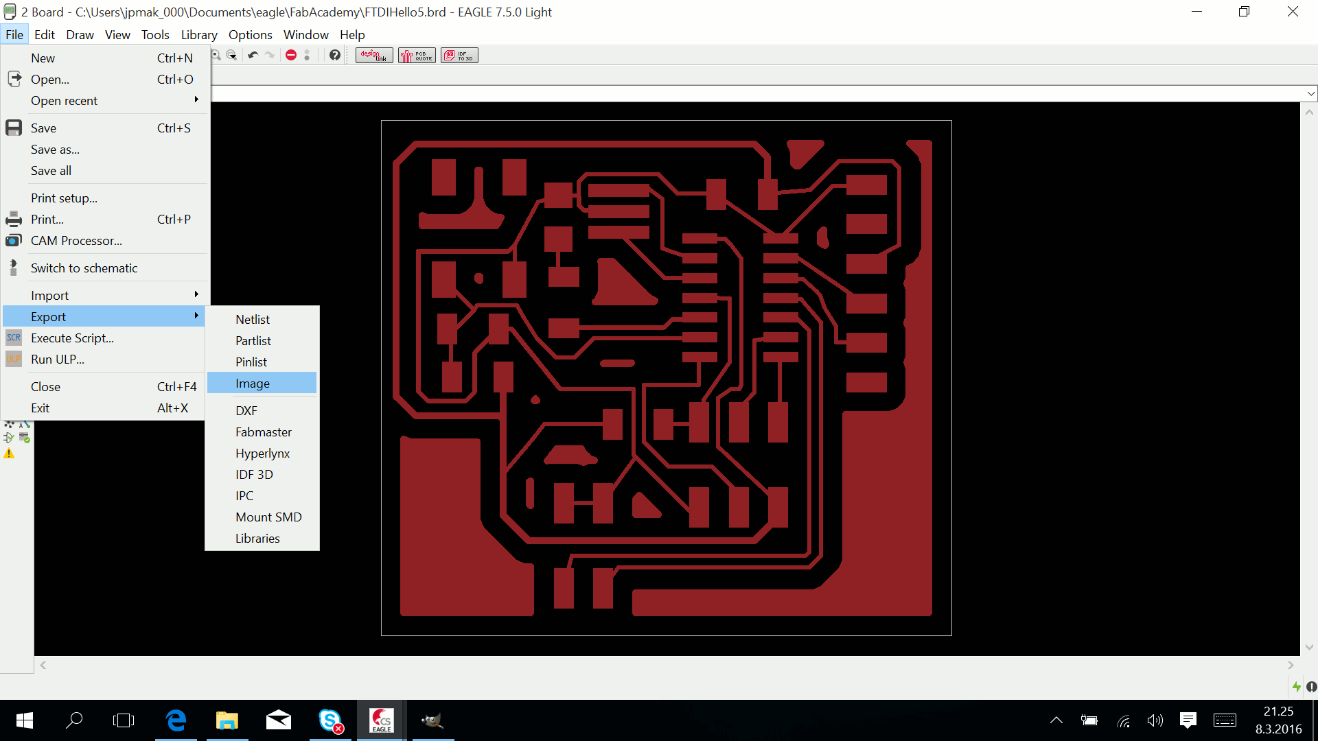
Processing in GIMP
Open the exported png file in GIMP
Add layer (make it black)
Select Layer boundary size created layer and add 1.6 mm to the current size (remember to center which is half of 1/32”)
Select Image layer- Fit Canvas to Layers. You can also re arrange the order of layers.
Color the outer “strip” to black with paint bucket . Be on the black layer for this one.
Export current image as png to be as trace routing file
Switch to traces layer and color it white which leaves the cutout trace and export that to png.
You can check with Scale image the size of the board
I used SMD pick and placer together with re-flow oven to make the make the board. Milling was easy by following the procedure presented in Assignment 4. You can see that one corner is not milled and the reason might be that the bed was not flat. However, that part of the board does not make a difference. NOTE!!!! The resistor R2 and capacitor C3 are wrong way around in the picture below. C3 should be “above” R2. The names on the board layout are miss aligned. This affects the button functionality.
Files: Board and schematic
