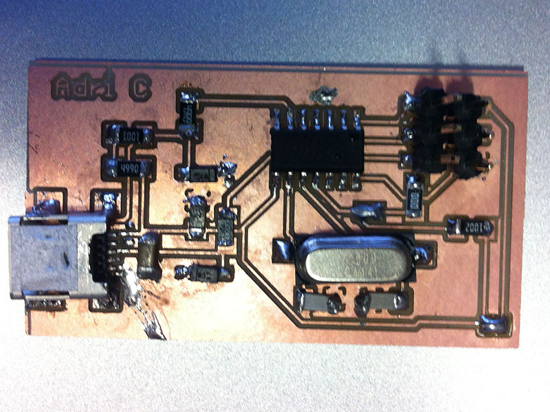
Fab ISP Board
I used the David layout for designing the Fab ISP.
I took only the components in the schematic view in order to do my own design.
I tried to eliminate the 0 resistor but it is for this moment not possible, I had to again use the 0 resistor and also, the board is bigger than the David Board.
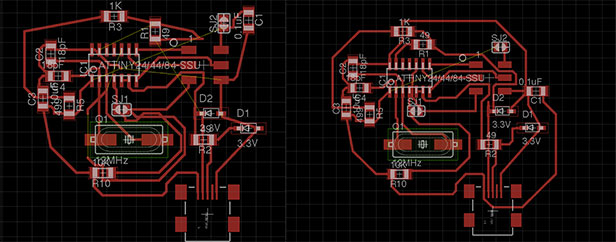
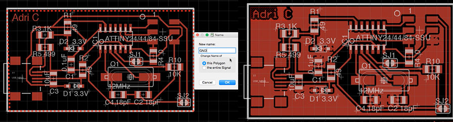
I used only the top part of the board, for optimizing the surface made of copper. Then I transformed the GND as main surface, as you can see in the following picture.
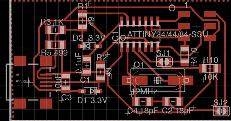
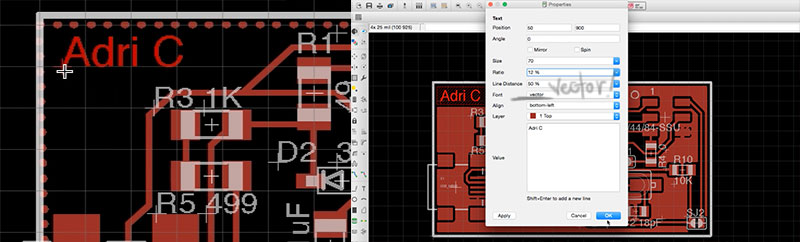
For writing text in the board, you have to select the top layer and also a Vector font in order to have enough space to mill the text. You can change the font in the Properties panel.
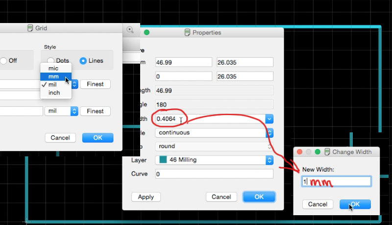
The milling layer is the last layer, which will separate the board from the basis. In this case you have to use another tool of 1mm for cutting. For this procedure, you have to verify the grid options and change the mill to mm. Afterwards, you can select the milling layer in the Properties panel and change the width for 1 mm and select the lines.
In the same layer you can build the bridge for fixing the printer into the platform. You can go to the Trim option and make a box as the picture shows.
Then remove the parallel vector and you can leave this layer for both sides open. When the board is finished you can easily break the board and polish the edges.
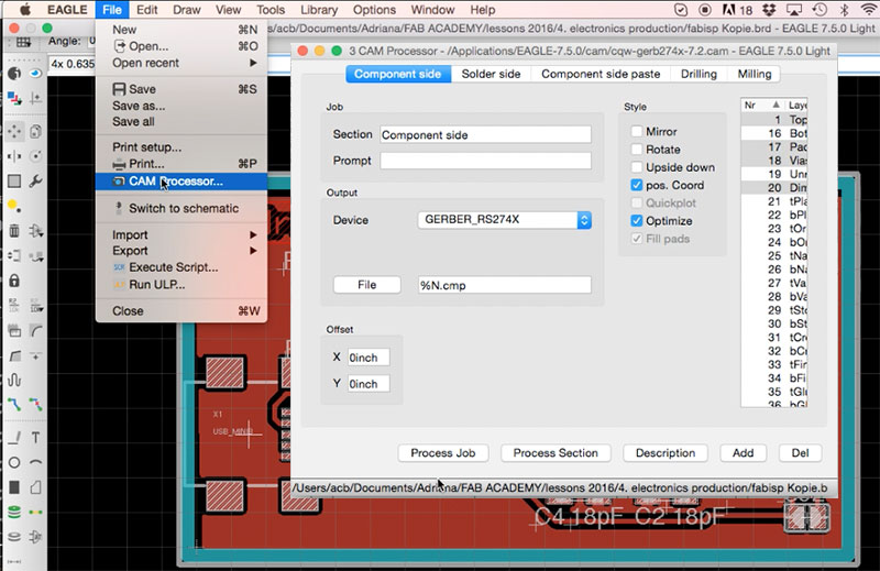
If this is the first time that you work with this program, you can go to the File options > Job > Open CAM Job > cqm-gerb-274x7.2 cam
the “gerb” o Gerber files are kind of “universal language” for PCB designs.
In this case I want to specify the gerber that I want to export.
About gerbers: Gerber files – note the plurality – each describe single layers of the PCB. One gerber might describe the silkscreen, while another defines where the top copper is. In all, we’ll generate seven gerber files.
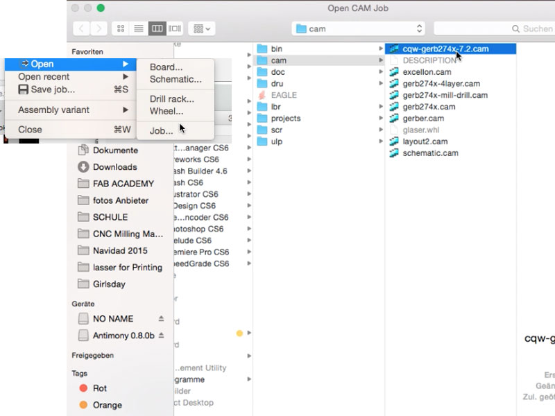
From here, go to the File menu, then go Open > Job…. In the file browser that opens, select the cqm-gerb-274x7.2 cam file that you just downloaded. Now the CAM processor window should have tabs: “Top Copper”, and basically the milling contour part. Each of these tabs define how to create one of the gerber files. Now all you have to do is click Process Job. If you haven’t saved recently, it’ll prompt you to.
Without closing this window, you can go to the Run ULP and select the option “mountsmd.ulp”. You are ready to mill your board.