FabAcademy2017 - Projects
Embedded programming
March 15, 2017 - Week#8
I have learned a lot from the Microcontroller Datasheet. I started working on embedded programming, after having an idea to make an Intelligent Robotic tracker, I decided to program microcontroller to interact with the environment around it. That is How I started my journey making robot with the following components; ATMEGA 328P, RaspberryPi, openCV Library, and Python2.7.
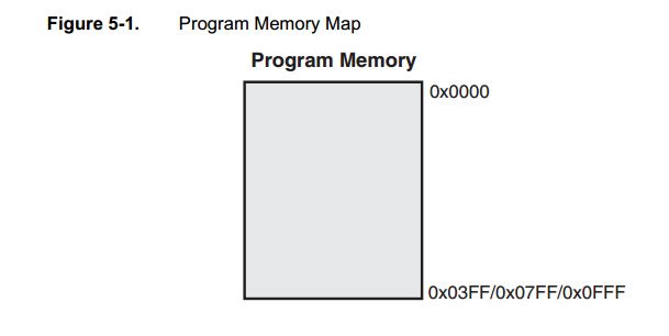
About Memory, I learned that the AVR architecture has three memory spaces that are linear and regular but it has two main memory spaces, the Data memory and the Program memory space. The third is an EEPROM Memory for data storage which the ATtiny24A/44A/84A features.
There is:
1. In-System Re-programmable Flash Program Memory
I have learned that The ATtiny24A/44A/84A contains 2K/4K/8K byte On-chip In-System Reprogrammable Flash memory for program storage. Since all AVR instructions are 16 or 32 bits wide, the Flash is organized as 1024/2048/4096 x 16
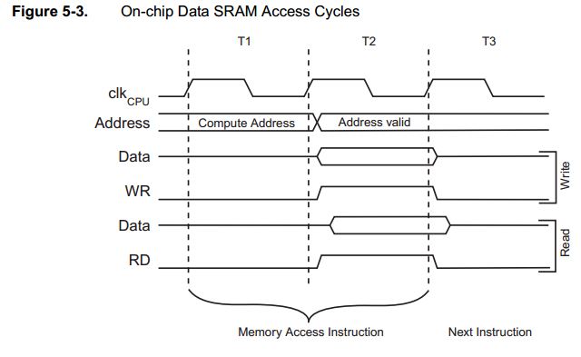
2. SRAM Data Memory
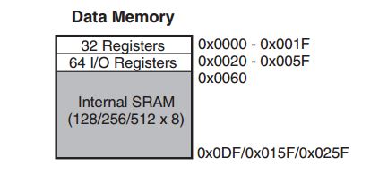
The figure below shows how the ATtiny24A/44A/84A SRAM Memory is organized
The Datasheet is split into 27 chapters that defines specific features. I read about the general overview, pins configurations and other general info about microprocessor in the first 3 chapters. Chapters from 4 to 19 describes about Input and outputs, memory programming, different chips features. Chapters from 20 to 27 give again general information of chips specifications, and registers, info about ordering, packaging, etc... At the end of the document Table on Contents is available.
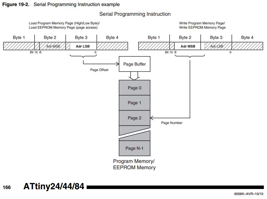
Serial Programming
Both the Flash and EEPROM memory arrays can be programmed using the serial SPI bus while RESET is pulled to GND.
Serial Programming Algorithm
When writing serial data to the ATtiny24/44/84, data is clocked on the rising edge of SCK. When reading, data is clocked on the falling edge of SCK. See Figure 20-4 and Figure 20-5 for timing details. To program and verify the ATtiny24/44/84 in the Serial Programming mode, the following sequence is recommended (see four byte instruction formats in Table 19-12):
1. Power-up sequence:
Apply power between VCC and GND while RESET and SCK are set to “0”. In some systems, the programmer can not guarantee that SCK is held low during power-up. In this case, RESET must be given a positive pulse after SCK has been set to '0'. The duration of the pulse must be at least tRST (the minimum pulse width on RESET pin, see Table 20-4 on page 177) plus two CPU clock cycles.
2. Wait for at least 20 ms and enable serial programming by sending the Programming Enable serial instruction to pin MOSI.
3. The serial programming instructions will not work if the communication is out of synchronization. When in sync. the second byte (0x53), will echo back when issuing the third byte of the Programming Enable instruction. Whether the echo is correct or not, all four bytes of the instruction must be transmitted. If the 0x53 did not echo back, give RESET a positive pulse and issue a new Programming Enable command.
4. The Flash is programmed one page at a time. The memory page is loaded one byte at a time by supplying the 5 LSB of the address and data together with the Load Program memory Page instruction. To ensure correct loading of the page, the data low byte must be loaded before data high byte is applied for a given address. The Program memory Page is stored by loading the Write Program memory Page instruction with the 3 MSB of the address. If polling (RDY/BSY) is not used, the user must wait at least tWD_FLASH before issuing the next page. (See Table 19-11 on page 165.) Accessing the serial programming interface before the Flash write operation completes can result in incorrect programming.
5. A: The EEPROM array is programmed one byte at a time by supplying the address and data together with the appropriate Write instruction. An EEPROM memory location is first automatically erased before new data is written. If polling (RDY/BSY) is not used, the user must wait at least t WD_EEPROM before issuing the next byte. (See Table 19-11 on page 165.) In a chip erased device, no 0xFFs in the data file(s) need to be programmed. B: The EEPROM array is programmed one page at a time. The Memory page is loaded one byte at a time by supplying the 2 LSB of the address and data together with the Load EEPROM Memory Page instruction. The EEPROM Memory Page is stored by loading the Write EEPROM Memory Page Instruction with the 4 MSB of the address. When using EEPROM page access only byte locations loaded with the Load EEPROM Memory Page instruction is altered. The remaining locations remain unchanged. If polling (RDY/BSY) is not used, the used must wait at least tWD_EEPROM before issuing the165 8006K–AVR–10/10 ATtiny24/44/84 next page (See Table 19-11 on page 165). In a chip erased device, no 0xFF in the data file(s) need to be programmed.
6. Any memory location can be verified by using the Read instruction which returns the content at the selected address at serial output MISO.
7. At the end of the programming session, RESET can be set high to commence normal operation.
8. Power-off sequence (if needed): Set RESET to “1”. Turn VCC power off.
What questions do you have?
For someone who has no experience of working with microcontrollers beforehand. Reading a datasheet is really hard to understand It leaves more questions. After reading more and doing some work with microcontrollers it will make more sense.
What would you like to learn more about?
I would like to go deeper into learning about memory and Serial Programming Algorithm
For More details, Here attached is microcontroller data sheet

I started with installing OpenCV Library and python 2.7 in the Raspberry Pi3 and connected to ATMEGA 328P microcontroller board I made from our FabLab, to be use on my face tracking robot.
Implementing programming protocols.
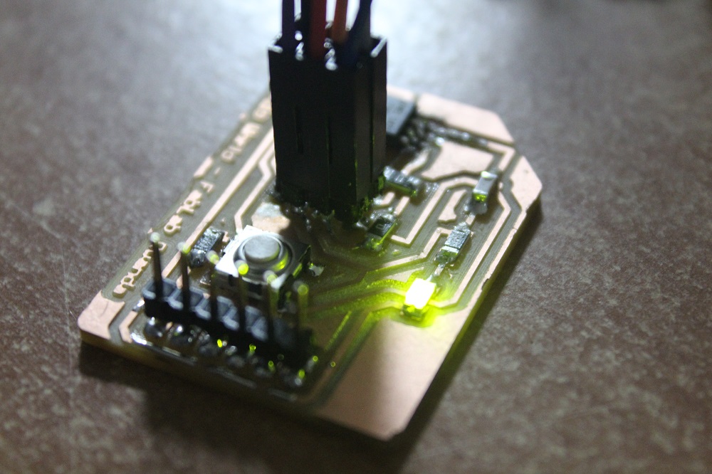
The chip I programmed is the one I made during the Electronics Design Week Assignment. The components I used are listed below.
Components used.
1. ATTINY45
2. 499 OHM Resistor
3. Green LED
4. Capacitor 100nF
5. Jumper (3)
6. 49 OHM Resistor
7. Switch button
8. 2x3 Pin header
9. 1x6 Pin header
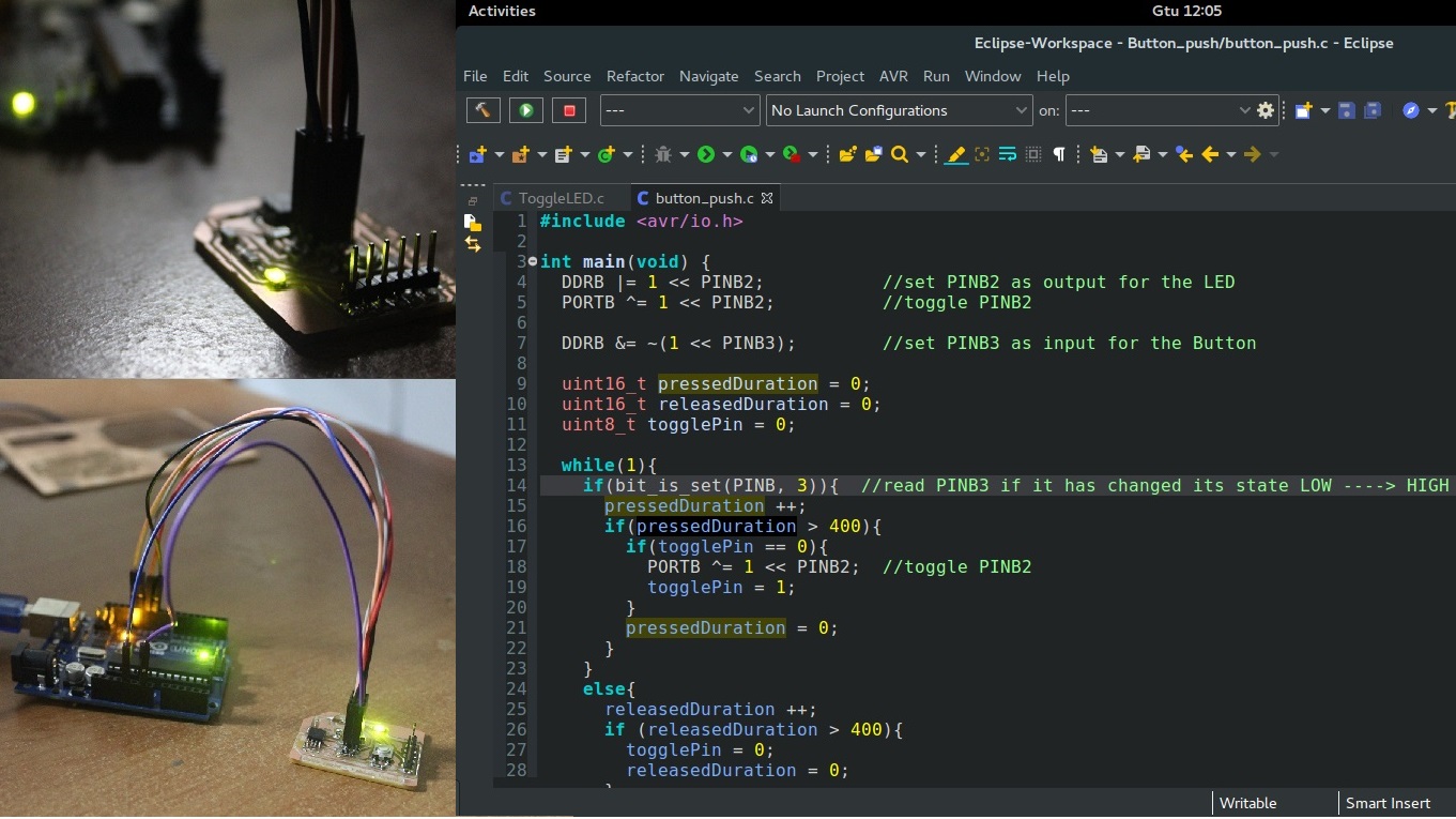
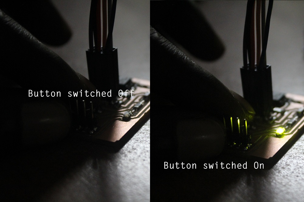
The board I made is able to read codes and execute the command. It has a Button and LED. The first time I uploaded the codes to make the LED light when I press the button, it failed. Later I discovered that I had made a mistake while soldering the board. The Ground wire and the reset were connected which was stopping the program commands from running.
After getting and correcting where the problem was, I connected my chip to the programmer and the programmer to my computer and I started the process of uploading codes to my chip. My Board is now able to light LED when the button is pressed. When I press the button again my LED turns off, and again the LED lights Green.
I attached here a video that shows how the button turns Off and On the Green LED on my board.
With An embedded programming language, Code is typically written in C or C++, but various high-level programming languages, such as Python and JavaScript, are now also in common use to target microcontrollers and embedded systems. My codes here below are written in C Programming
/*This is my codes to light LED as you push a button.*/ #includeint main(void) { DDRB |= 1 << PINB2; //set PINB2 as output for the LED PORTB ^= 1 << PINB2; //toggle PINB2 DDRB &= ~(1 << PINB3); //set PINB3 as input for the Button uint16_t pressedDuration = 0; uint16_t releasedDuration = 0; uint8_t togglePin = 0; while(1){ if(bit_is_set(PINB, 3)){ //read PINB3 if it has changed its state LOW ----> HIGH pressedDuration ++; if(pressedDuration > 400){ if(togglePin == 0){ PORTB ^= 1 << PINB2; //toggle PINB2 togglePin = 1; } pressedDuration = 0; } } else{ releasedDuration ++; if (releasedDuration > 400){ togglePin = 0; releasedDuration = 0; } } } }
In my Final Project I chose to work on a robot so, I have to control servo motors, That's why I put here codes I have to use as also part of embedded programming expected in my final project.
/*This is my codes to light LED as you push a button.*/
      #include

char tiltChanel=0;
char panChanel = 1;

#define pinTilt 8
#define pinPan  9
#define lightPin 7

Servo servoTilt, servoPan;

char serialChar = 0;

void setup() {

  servoTilt.attach(pinTilt);
  servoPan.attach(pinPan);

  servoTilt.write(90);
  servoPan.write(90);

  //setup pin 7 mode
  pinMode(lightPin, OUTPUT);

  Serial.begin(57600);

}

void loop() {
  // put your main code here, to run repeatedly:
  int ldr = analogRead(A1);
  Serial.println(ldr);

  if(ldr > 800){
    digitalWrite(lightPin, HIGH);
    Serial.println("Dark Detected");
  }else {
    digitalWrite(lightPin, LOW);
    Serial.println("Light Detected");
  }


  while(Serial.available() <= 0);
  serialChar = Serial.read();

  if(serialChar == tiltChanel){
    while(Serial.available() <=0);
    servoTilt.write(Serial.read());
  }

  else if(serialChar == panChanel){
    while(Serial.available() <= 0);
    servoPan.write(Serial.read());
  }

}
The circuit:
* LED attached from PORTB2 to ground
* pushbutton attached from pin 2 to +5V
* 10K resistor attached from pin 2 to ground
Each time the input pin goes from LOW to HIGH (e.g. because of a push-button press), the output pin is toggled from LOW to HIGH or HIGH to LOW. There's a minimum delay between toggles to debounce the circuit (i.e. to ignore noise).