FabAcademy2017 - Projects
Electronics design
March 01, 2017 - Week#6
I started Electronics Design after Electronics production, this was helpful to me, because learning electronics production gave me some experience which was required to work on electronics Design. I tried to visit different sites to find where I can have a guide to design a board well.
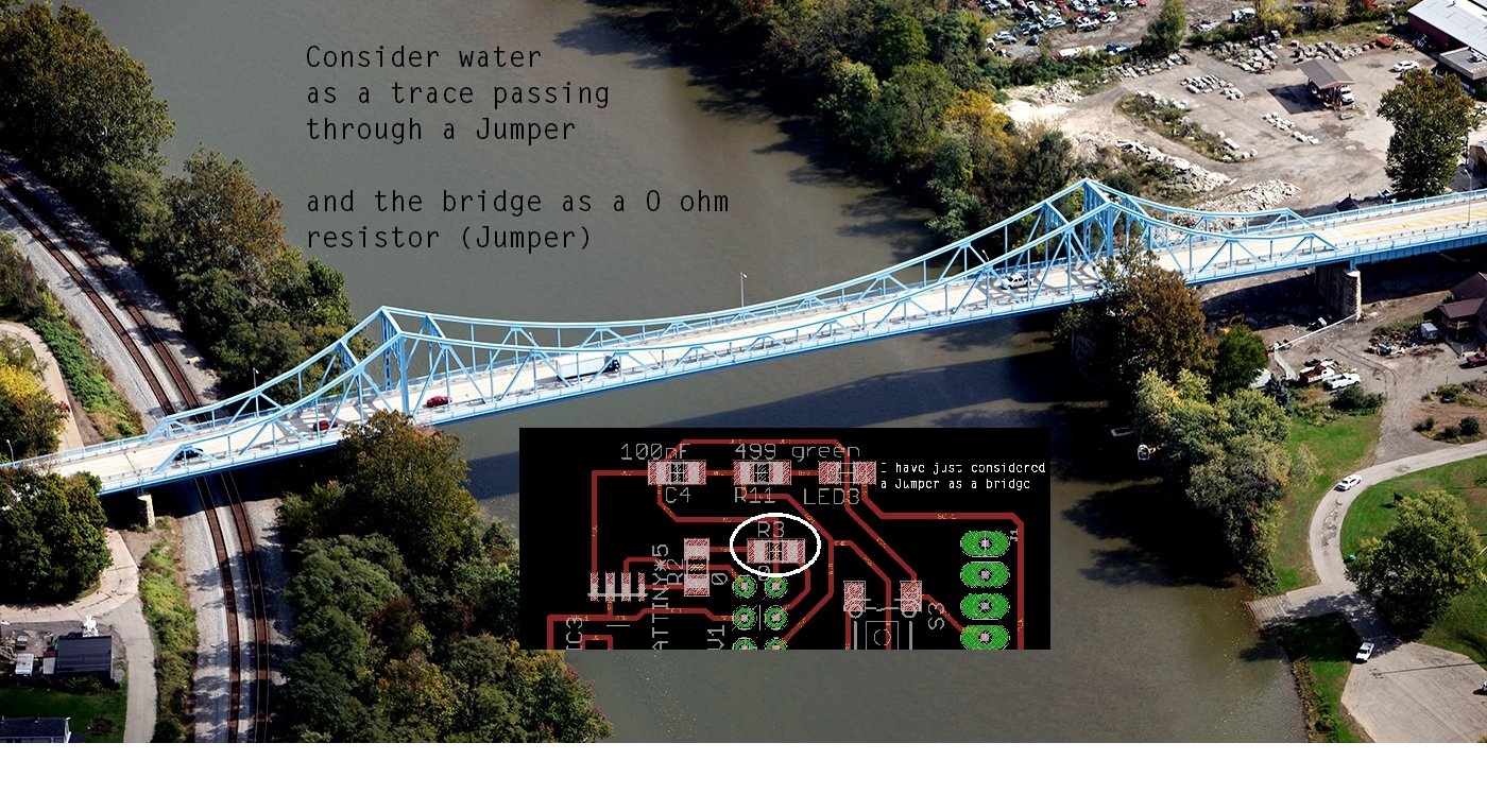
In the Hello world board I Designed, the first challenge I met was that It was complicated to know where I am going to pass some traces connecting to the components, but later I used jumpers, after meeting that challenge and I just learned that Resistors of 0 OHM (Jumpers) act as just a bridge where you need to pass something up and down.
Here are the four basic views in Eagle: Schematic, Board, Library, and Control Panel.
Schematic - the schematic for your project is drawn there and it where you are able to define the parts to use in your board.
Board - Here you physically connect and modify the pins you defined in the schematic, and you can lay out the pieces in your board.
Library - With Library you can edit and manage parts.
Control Panel is the main window, it launches other windows, when you close it, you close all windows opened.
Description about the workflows used in circuit board design
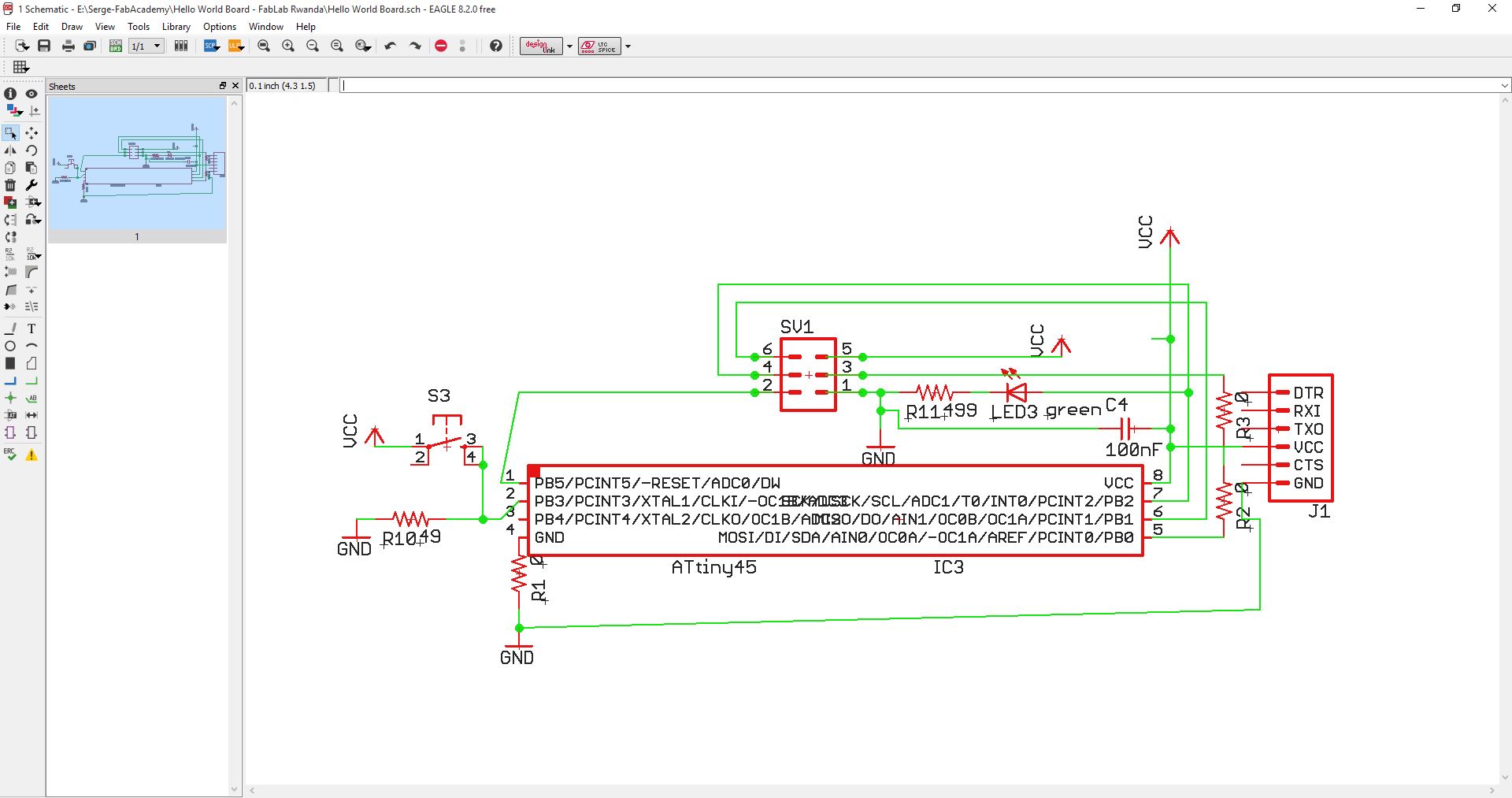
Components used.
1. ATTINY45
2. 499 OHM Resistor
3. Green LED
4. Capacitor 100nF
5. Jumper (3)
6. 49 OHM Resistor
7. Switch button
8. 2x3 Pin header
9. 1x6 Pin header
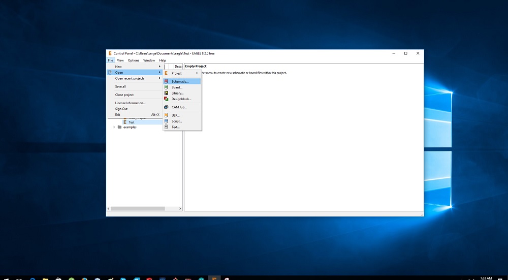
I had to install the pcb design tool. So, first installed Eagle software.
Eagle tip and tricks
1. In Eagle you can use commands from Menu, from top and left-hand toolbars, or from command line. Move the mouse over the icons on the toolbars to see the names and what they do.
2. Do not place anything below or to the left of the cross (origin) in either schematic or layout when you use the free version of Eagle.
3. To change the background color of the schematic/layout, from Options > User Interface...
4. You can use Autorouter to obtain automatic routes for the circuit.
Creating the schematic
To create a new schematic Select the project in the left-hand tree, File > New > Schematic Save the schematic with a descriptive name
Add components from fab.lbr library and/or other libraries (e.g., supply1)
First download the fab.lbr and activate it to get most of the Fab Lab inventory components.
Now you can import fab.lbr in your eagle software. On the left side of the panel, click the Libraries. This will open a tree showing all available libraries. You click on the Browse to import it from your downloads directory. now your fab lab components are imported.
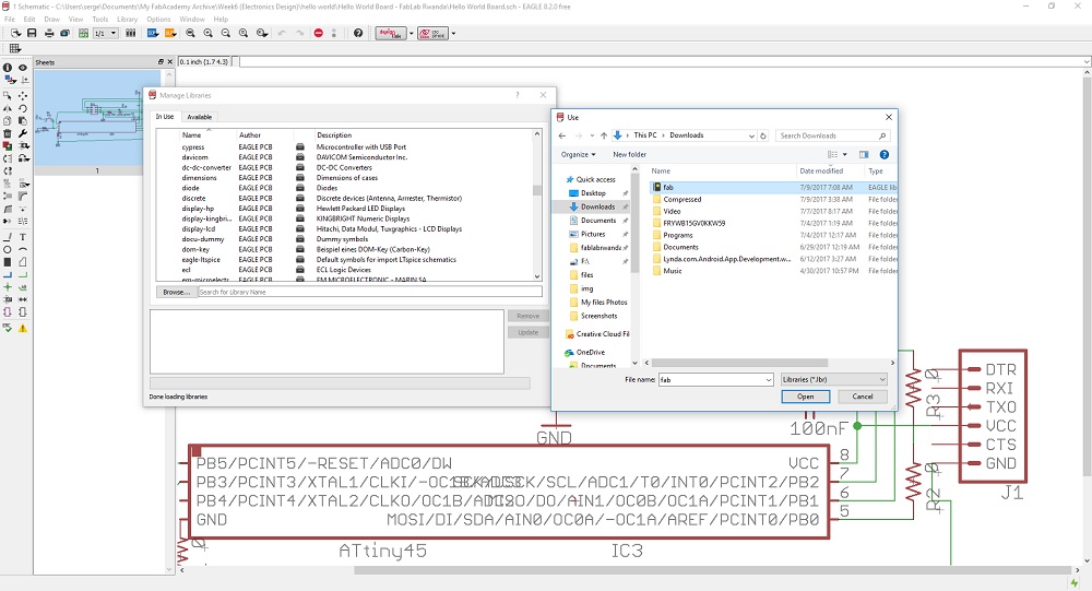
Add components from fab.lbr library In the schematic window: Select the “Add” icon from the left-hand toolbar Open “fab” library and select the desired component
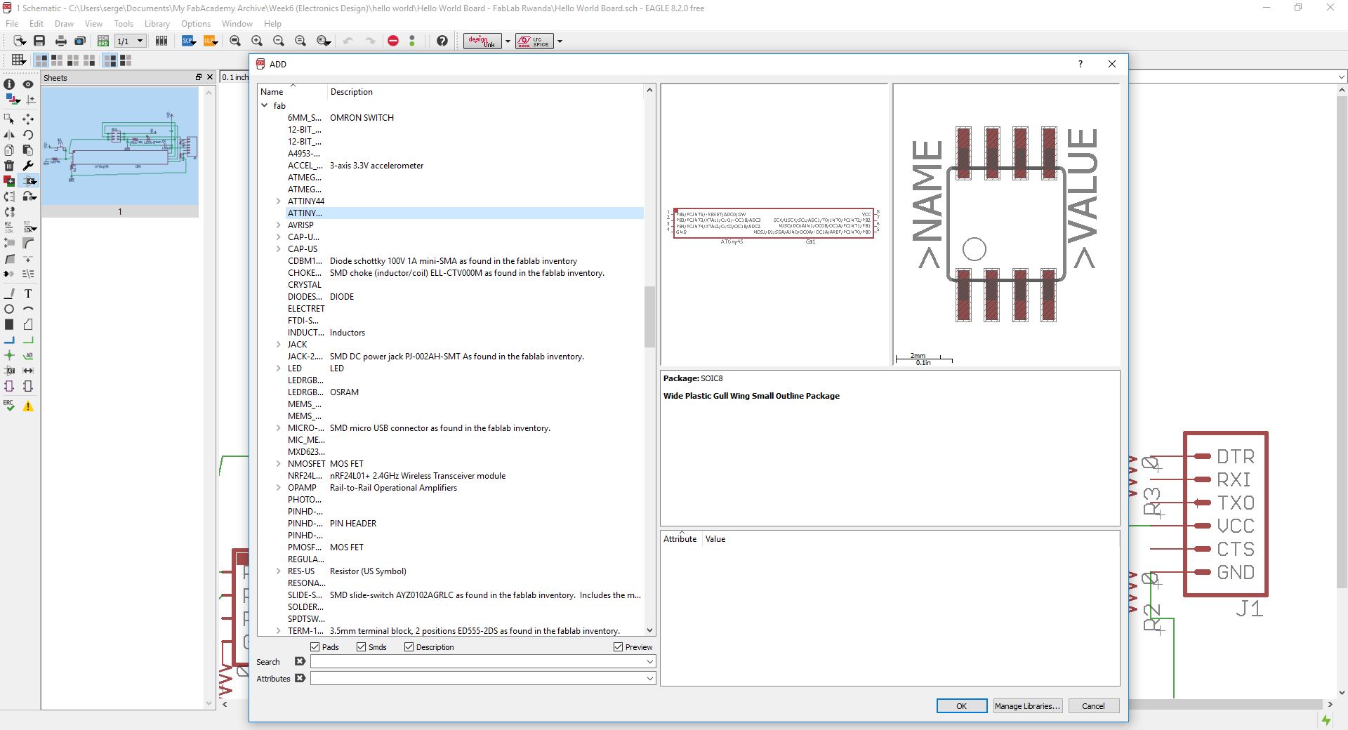
Press OK
And click on the schematic to place the component. Later you can move the components using the button “Move”. To add supply (VCC) and ground (GND) components Use the library supply1. Connect the components using Net button Check the consistency of electronic rules Click ERC to check the schematic for electronic rules errors Correct the errors and switch to the board layout design
My model of schematic for the PCB I wanted to create is the following:
Creating the board layout
From Schematics view switch to board layout using the “Generate/switch to board” button in the top toolbar
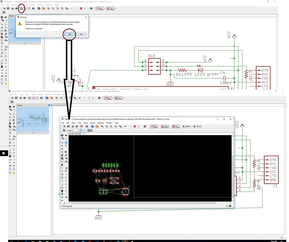
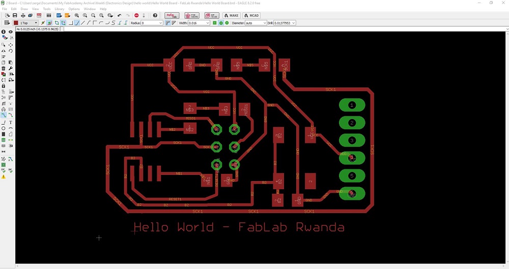
Move components into the board area Connect the components using Route button Check for consistency (check design rules, DRC) The final board layout could look like this:
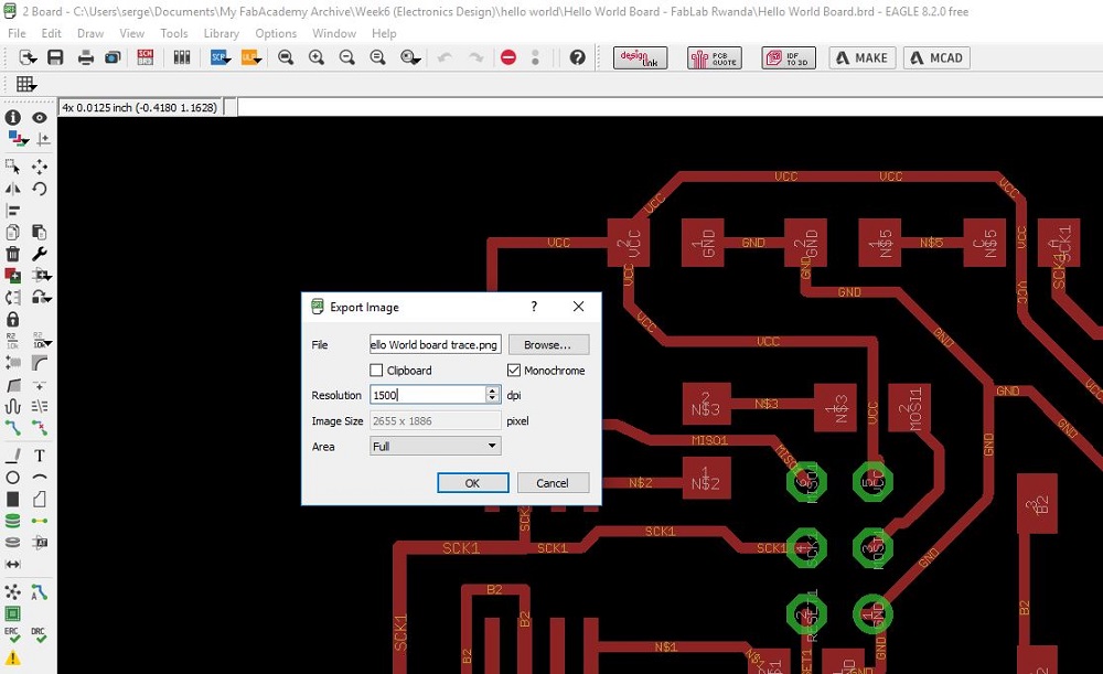
Export the board layout in png format Export the top layer design from Eagle into an image .png with resolution 1500 dpi and monochrome. View > Layer settings ... > None; 1: Top (to select only the top layer of the layout) and then File > Export as… and select the parameters in the picture below:
Attached here are tutorials on Eagle: http://www.autodesk.com/products/eagle/overview )
http://archive.fabacademy.org/archives/2016/doc/electronics_design_eagle.html.
https://wiki.oulu.fi/display/FLOWS/Electronics+design+and+production.
https://learn.sparkfun.com/tutorials/using-eagle-schematic.
https://www.sparkfun.com/EAGLE.
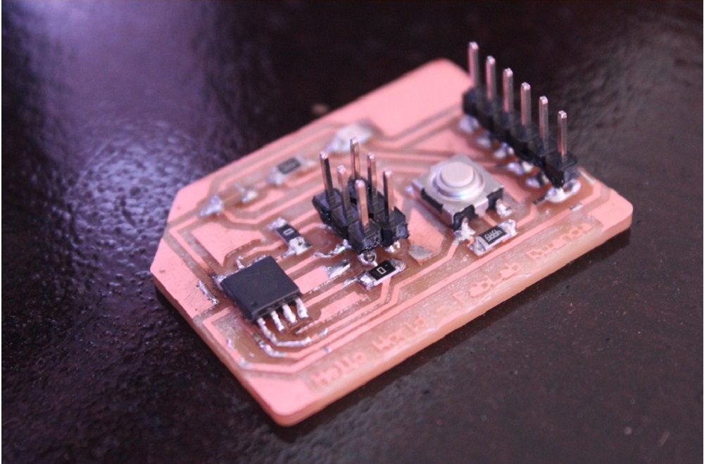
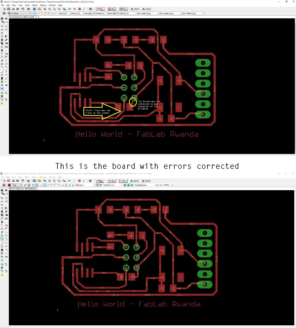
When I was designing connecting pins, there is one that I just jumped, I just found that i jumped one after soldering. So, I had to find how to fix that, I decided to use soldering wire to connect where it is need and disconnect where necessary. Ground was not connected to the ISP Pins, and the jumper was touching on the trace connecting to ISP Pins.
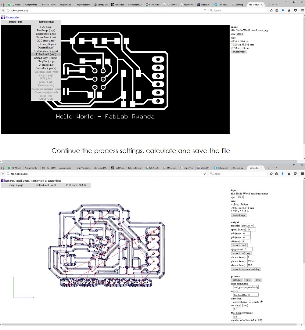
Here are steps in fabmodules to generate Roland mill files for CNC milling machine to read them, I generated
Trace.rml file with 1/64 tool and Outline.rml file with 1/32 tool.
I had to gently remove the circuit board from the bed milling machine to clean it.

The circuit was ready after milling. Then, I had to solder it putting all the components needed for Hello World Board.