Week #6 Electronics Design
Assignments
Software Used
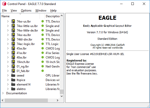
- EAGLE 7.7.0
- GIMP2.0
- Roland VPanel for MDX-40A
- Fab Modules
Machine Used
- CNC Router Roland MDX-40A
Exercise Repo
You can find all files used in this class in the Fab Academy repository in the button below or a backup in this Google Drive folder.
Past experience
As I said on the exercise 04 page, I had already done one PCP for a Astável multivibrator, when a student teached me how to design the board on Eagle.
Log
2017 03 02 Eagle Tutorial
I started by doing the Hello World Eagle tutorial. First thing I did was to install the libraries "01_fab.lbr" and "01_ng.lbr", and checked if it was availabe on the software.
But when I opened the "hello.sch" I noticed that the schematic was organized differently than the one shown in tutorials image. But, it should be ok!
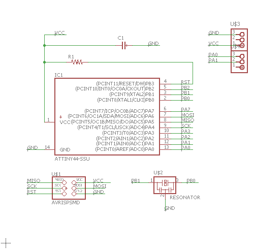
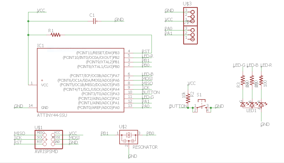
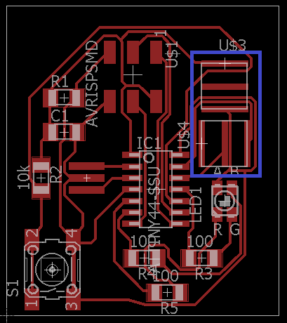
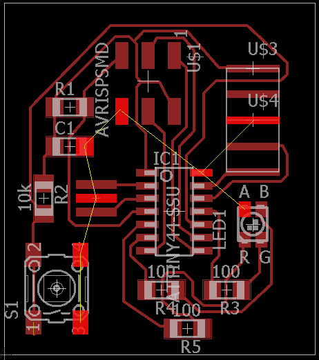
As are said in the tutorial, the hello.sch file already have:
- 1 6-pin programming header: for programming the board
- 1 Microcontroller ATtiny44A
- 1 FTDI header: powers the board and allows board to talk to computer
- 1 Resonator 20MHz: external clock
- 1 Capacitor 1uF
- 1 Resistor 1206 10 ohms
So, I added:
- 1 Button OMRON switch;
- 1 Resistor 1206 10k ohms
- 1 LED RGB P-LCC-4
- 3 Resitor 1206 499 ohms
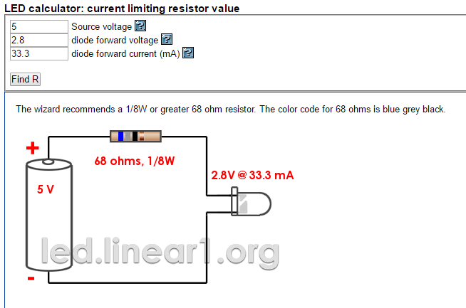
To calculate witch resistor I should use to don't burn out the LED, I used the. LED calculor. To get the values to use in the calculation, I looked at the datasheet found on Digi-Key website. As I'm using a LED RGB, the Forward Voltage varies with color (R= 2.0 V, G= 3.2 V, B= 3.2 V), as well as Forward Current (R= 50 mA, G= 25 mA, B= 25 mA). Then I did the calculation separeted for each color and the resultants resistors were R= 68 ohm, G= 82 ohm and B= 82 ohm. I deciced to use a 499 ohms resistor because was the closer one I have available.
After choose and add all components, I connect them, as seen in the image below.
2017 03 03 Eagle Tutorial (continue...)
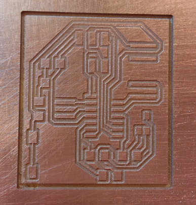
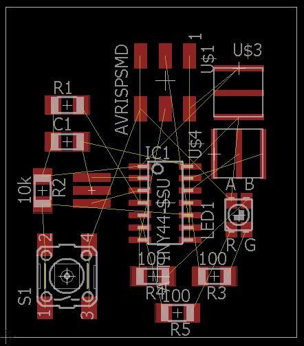
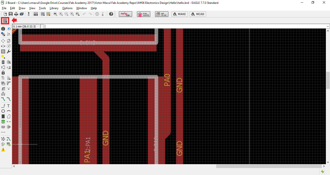
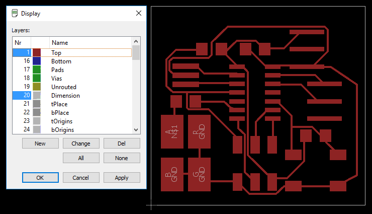
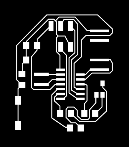
Then I switch to board, organized the components and used the autorouter feature. After experiment some scenarios with autorouter feature, I found a good one (I just had to to move one trace to leave more space between traces). To verify if the space between traces were good, I used the grid on my display, and setted the size 0.1mm (my tool diameter).
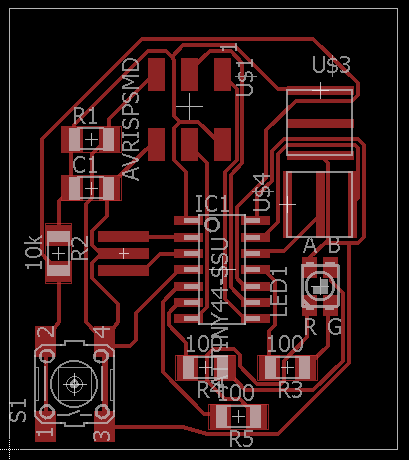
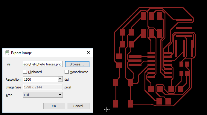
With the traces routered, was time to export the png file. To do this I selected just the "Top" and the "Dimenson" layers.
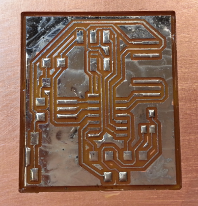
2017 03 09 Making the PCB and soldering the components
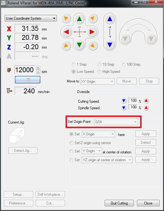
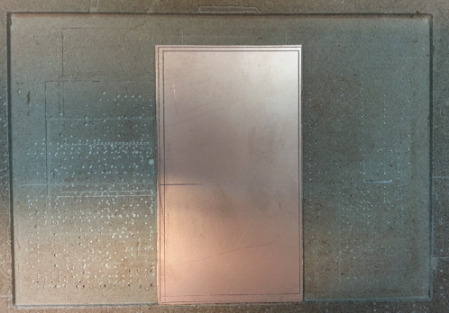
I did procedures from exercise 04 to produce the PCB. But, in this time I had I had an issue with origin setting. I did the procedure using a different coordinate system at Roland VPanel (when we use the Cooper CAM software, it uses G54 coordinate system to set origen, and I didn't notice that is was the that was selected). For Fab Modules, the right one to use is User Coordinate System. The pictures below show where is this opition and the result that I had using the wrong coordinate system.
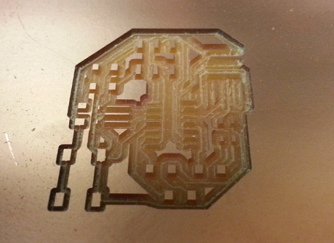
Even adjusting the oringin, I was still having troubles to mill PCB traces. Then I got a knew tool and defined the Z origin 0.1mm above (as my tool is conical, defining the Z origin uper, the diameter became smaller). The next step was to check if the table was leveled. To do this move the Z to -0.15 and I milled around the perimeter of the board manually, using the control panel. I did it in different zones of the table to find a better place to position my board. The pictures bellow ilustrate my results.
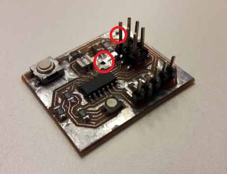
After that, I was gathering the components to solder on my board and noticed that I I made a mistake: I separeted the 2 components that represents FTDI header, and positioned them with different orientations.
Then, I started againg positioning the components and tracing routes. This time I decided to work with just 5 pins on FTDI header. Doing this I could use overlap two of them to ensure the right spacing between them. Another option (smarter one, but I just think on that latter) would be to change both 3-pin header by a 5-pin header. When I was doing the routes, I got stucked in the last ones. Then I decided to use my board as GND, instead trace a route between that components. To do this, I just deleated GND pads on GIMP.
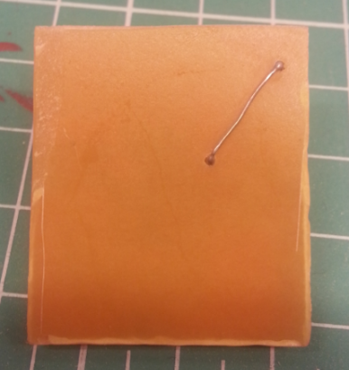
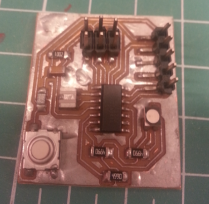
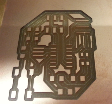
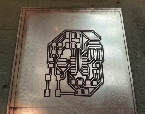
After correct this issues I repeated the process and fabricated a new board. Then, I solder the components following the procedures described on exercise 04. When I did the continuity test with the multimeter I noticed that one of GND conection was not working. I fixed this issue by adding a jumpper on the oposite side of my board. The pictures bellow ilustrate this process.