Week #4 PCB fabrication
Assigments
Software Used
- GIMP2.0
- Roland VPanel for MDX-40A
- Fab Modules
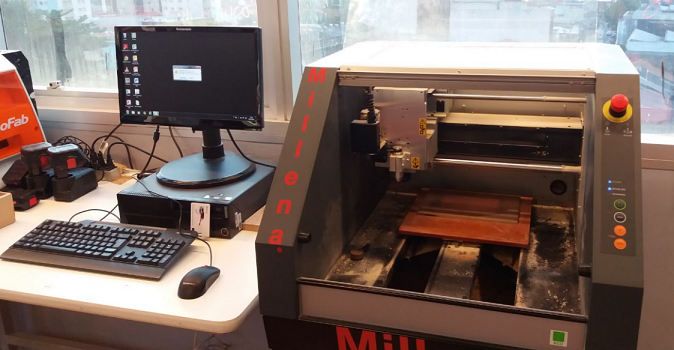
Machine Used
- CNC Router Roland MDX-40A
Exercise Repo
You can find all files used in this class in the Fab Academy repository in the button below or a backup in this Google Drive folder.
Past experience
I had already done one PCP for a Astável multivibrator. A student teached me how to design the board on Eagle, than a colleague teached me how to mill the PCB. Then another colleague teached me how to assemble a breadboard to prototype the the circuit, how to solder, how to perform the continuity test with a multimeter, and a little more about electronic components and how to read a electronic layout. First time it didn't worked because I design it wrong on Eagle. Then, I correct the file and made it using Fab Modules, with a help of our local instructor Kenzo.
Log
2017 02 19 Making a PCB
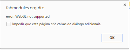
To make my in-circuit programmer board I followed Brian's documentation, titled "Building the FabTinyISP". First step was generating the rml files on Fab Modules. I had an issue in opening Fab Modules page on Google Chrome. I would recomend to use Mozilla Firefox for it.
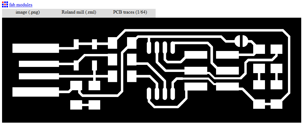
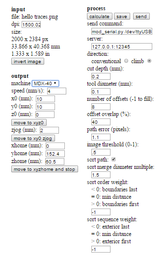
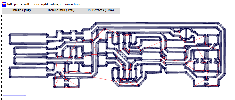
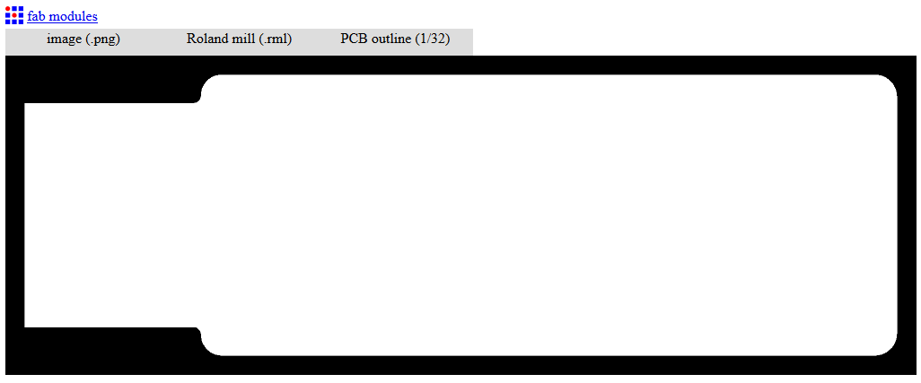
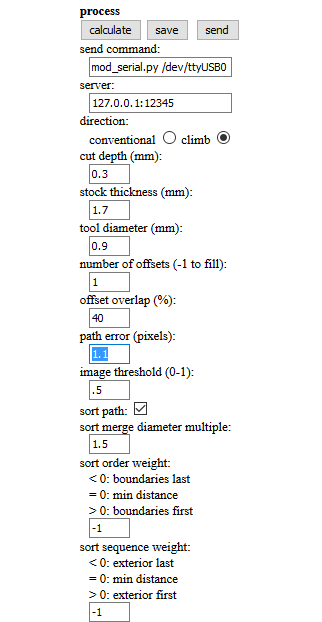
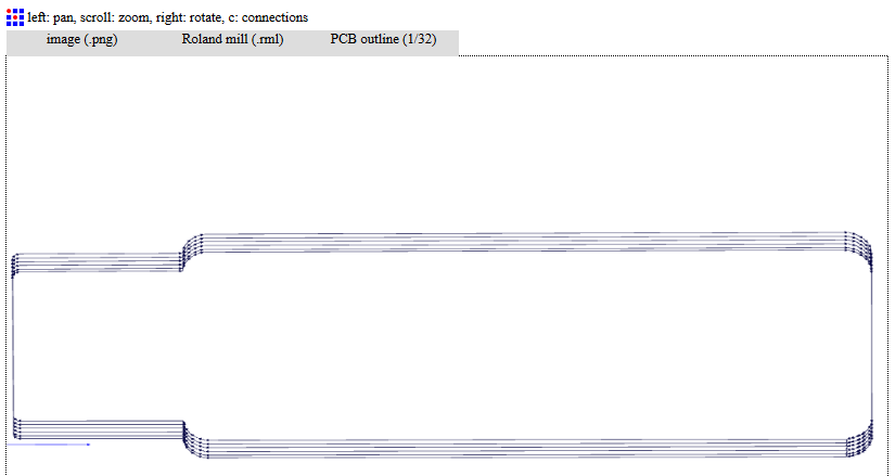
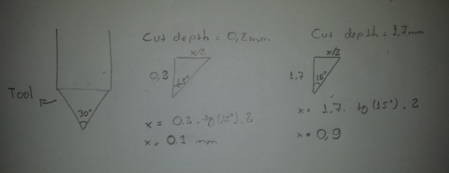
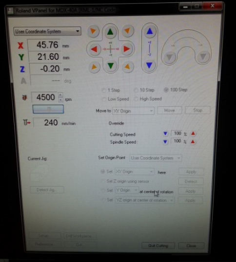
I found Fab Modules easy to use. There are just 5 simple steps: (1) Select input format; (2)Select output format; (3) Select the process; (4) Set parameters and calculate; (5) Save or send to machine. For this assigments I used as the png files (1), provided in the Brian's documentation. The output file for doing PCBs on Roland mill is rlm (2). To make a PCB for SMD components you just have to do two operations: PCB traces and PCB outline (3). The first I did was PCB traces, then outline. The parameters I've used are showed in the figures below. To calculate the tool diameter, we use tan(15) As my notebook was not connected on the machine I saved the rml fliles in a pendrive (5).
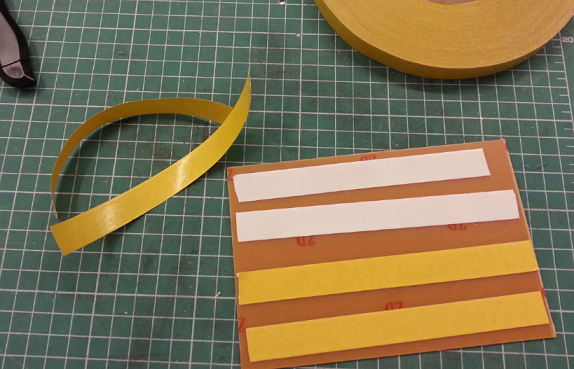
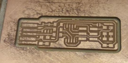
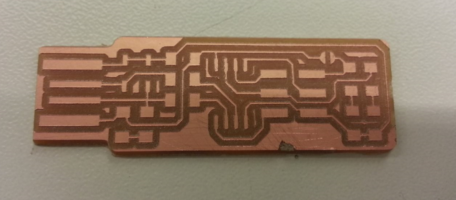
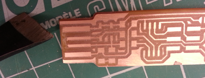
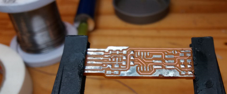
With the rlm files saved, the next steps are to set origins on the machine, mill the taces and the outline cut. To set Z origin I used the sensor. The XY origin was setted by eye. After milling, I used a sandpaper to clean the PCB traces. The pictures below shows this process.
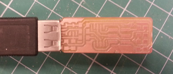
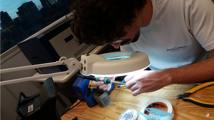
With PCB made, time to soldering! This was my first time sin soldering SMD components. The first thing I did was to apply fluid and tin in all traces. I think that it makes soldering SMDs easier. I had a little difficult in doing it in the begining, but on the third one I was satarting to be more familiar with this process. The pictures bellow shows how it was, and my results.
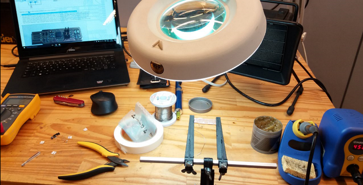
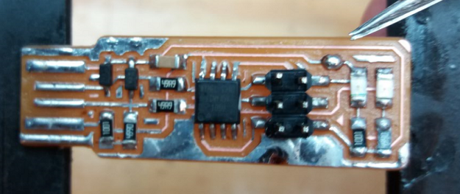
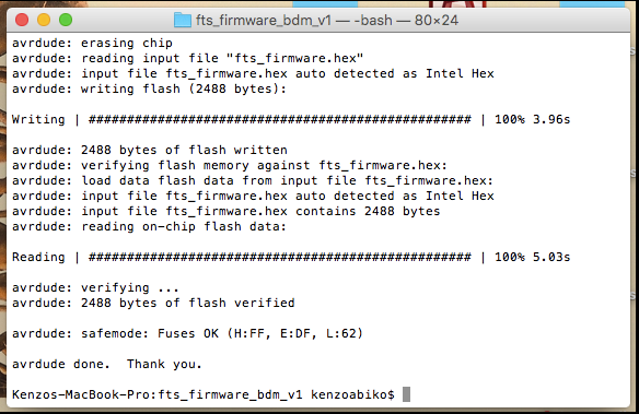
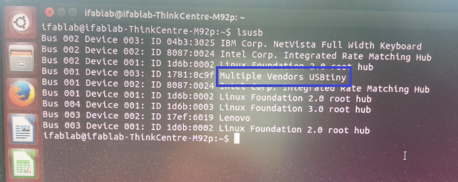
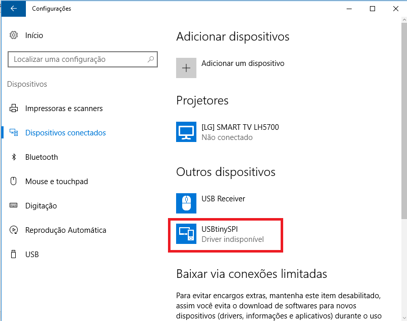
With the all components soldered on the board, the next step was to programme the board. I did it with Kenzo, our local instructor, in his Mac. After doing the procedures, we were not able to identify the board on Mac, neither in Windows 10. In Linux it was sometimes working, sometimes not. I put more tin on the USB connection part of board, a leveled it with a file, and also better cleaned the board with isopropyl alcohol. After that, the PCB worked well! Then Kenzo and me did the last step on programming (Blow the Reset Fuse) and removed the bridge on the solder jumper.
To Do:
- Programme a board with my FabTinyISP