- Week 6 +
electronics design
Tasks
For the given task of redesigning the hello.echo.world board, I have decided to use a widely used schematic and PCB design tool known as EAGLE, which is an acronym for Easily Applicable Graphical Layout Editor.

I am working on the version 7.6.0 to design the board. Here is the steps on how I redesigned the hello.echo.world board and added new components (pushbutton and LED) to it.
To begin with, I referred to the official design of the hello.echo.world board to identify the components used in it.
I was able to identify the following components:
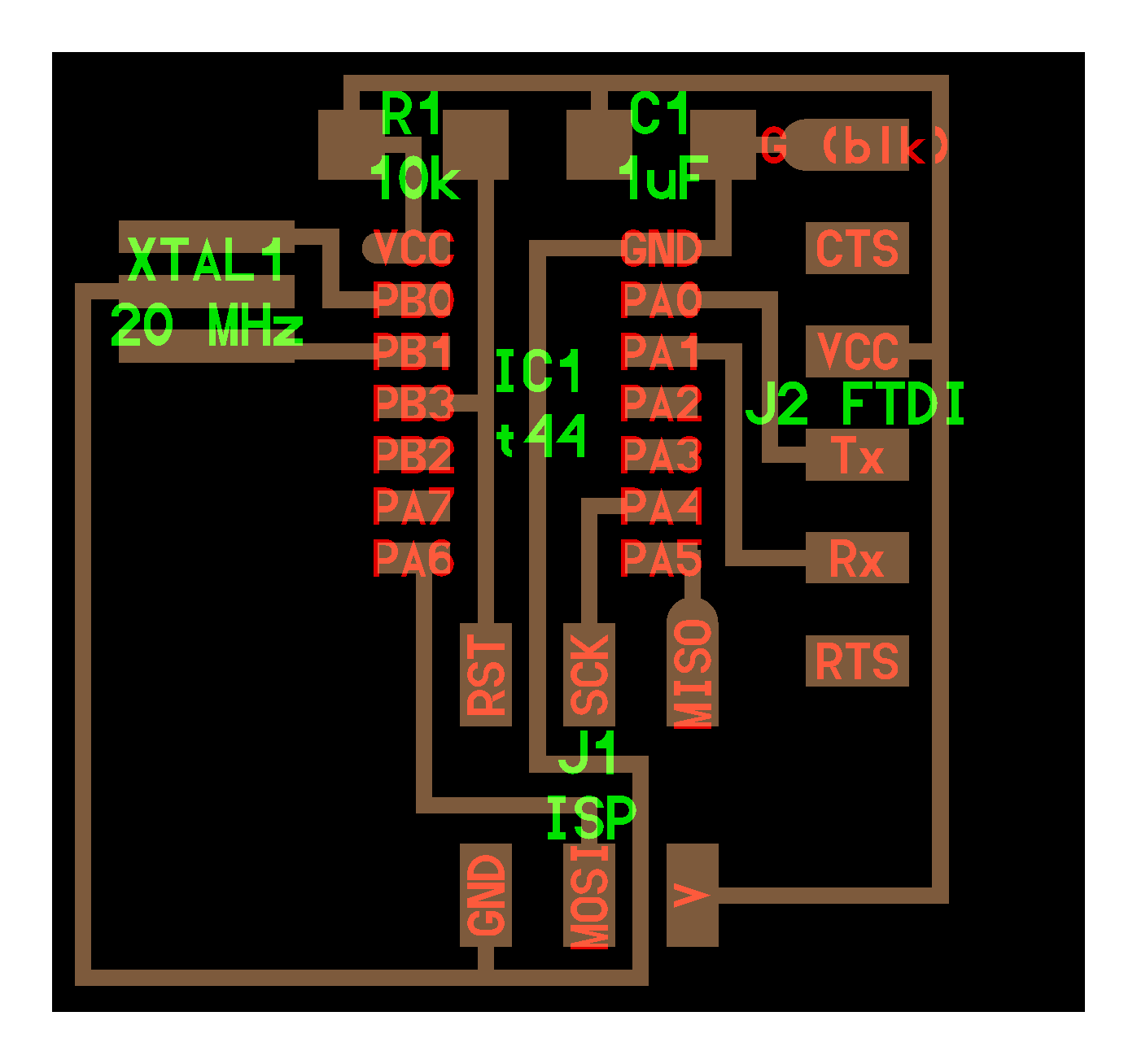
1. 1 x ATTiny44 Microcontroller : The brains of the board, this is the part that can read/write analog/digital data and input/output it on its pins.
2. 1 x 20 MHz Resonator : The clock of the brains, keeps everything in sync and stabilises the timer of the microcontroller. The value 20 MHz implies that the oscillations occur 2,00,00,000 times in one second.
3. 1 x AVR ISP header : The link between the programmer and the microcontroller. This part connects to the programmer and accepts code from the computer. It consists of the following pins:
a. MOSI - Master Out Slave In
b. MISO - Master In Slave Out
c. SCK - Serial ClocK
d. RST - ReSeT
e. VCC - +5V
f. GND - GrouND
4. 1 x 10k Ohm Resistor - This is a pull-up resistor for the Reset pin so that it doesn’t stay as a floating pin and randomly reset the microcontroller.
5. 1 x 1uF Capacitor : This component is used to smoothen the peaks and troughs in the power supply. It’s a good safety feature to incorporate in the circuit.
6. 1 x FTDI header : The FTDI header is provided so that Serial Communication can be established with another microcontroller using a USB to TTL converter like an FTDI cable or FTDI Breakout board.
As a part of the assignment, we were also supposed to add the following components:
1. 1 x Pushbutton : The basic use of the pushbutton is to sense if it is pressed or not
2. 1 x LED : The LED can be connected to a digital pin and can be controlled to do whatever a person desires to do with it: send morse codes, use as an indicator, use it as a fairy light etc.
3. 1 x 1k Ohm Resistor : This resistor is used as a current limiting resistor, which means that it will decide the flow of current, and thus, the brightness of the LED attached to it. The reason that such a high value of 1K was chosen was because the SMD LEDs tend to be extremely bright and start heating up with lower current-limiting resistor value.
Circuit Board Design
After identifying all the relevant components, I followed these steps to redesign and add the extra components:
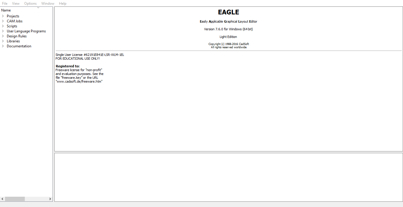
Step 1: Start Page for Eagle
This is the control panel of eagle, that appears as soon as you start eagle. These are the things that are visible on the page:
a. Documentation: This contains help files regarding various steps in creating pcbs. It is a useful reference.
b.Libraries: The component libraries are supplied with EAGLE and contain the footprint and pinouts of various components. Additional new libraries can be found at element14.com and similar sites. For the fabacademy circuits, library file can be accessed here.
c.Design Rules: All the parameters relevant to the board and its manufacture are specified in the Design Rules. The layout can be checked any time with the aid of the Design Rule Check (DRC command). These rules are also valid for the Autorouter. For creating appropriate traces, DRC file can be accessed here.
d.User Language Programs: These programs are real applications which, of course, show the abilities of the EAGLE User Language.
e.Scripts: Script files are a powerful tool. They can contain long sequences of commands, such as the specification of specific colors and fill-patterns for layers. Since every EAGLE operation can be carried out with the help of text commands, you can, for example, import data or configure EAGLE with the aid of script files.
f.CAM Processor: The CAM Processor provides a job mechanism with the aid of which the creation of the output data for a board can be automated.
g.Projects: This is Menu which contains two submenus which contain custom projects as well as example projects.
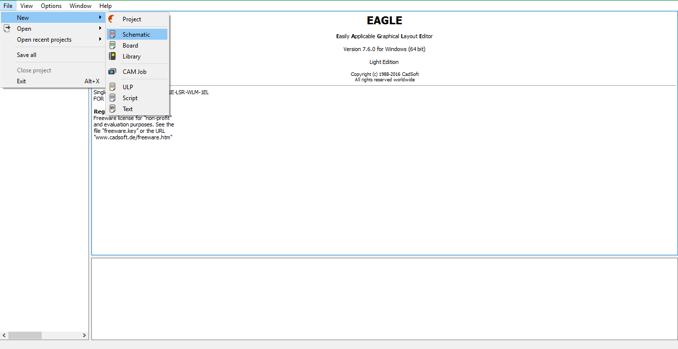
Step 2: Choosing schematic from menu
Navigate to File > New > Schematic to begin a new schematic file. This file will contain details about how each component connects with other components.
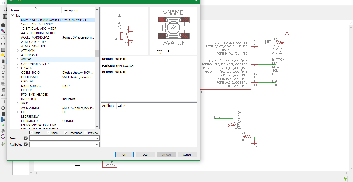
Step 3: Adding components
Now, EAGLE 7.6.0 provides a command-line interface as well as a GUI for ease of users. I prefer the GUI over the CLI.
For adding relevant components to the schematic, click on this icon in the left vertical menu:

This allows you to add new components for the schematic. For our use, we will select the fab library and choose our components from it. When you click on a component, its schematic symbol as well as its pcb footprint is shown along with other relevant details.
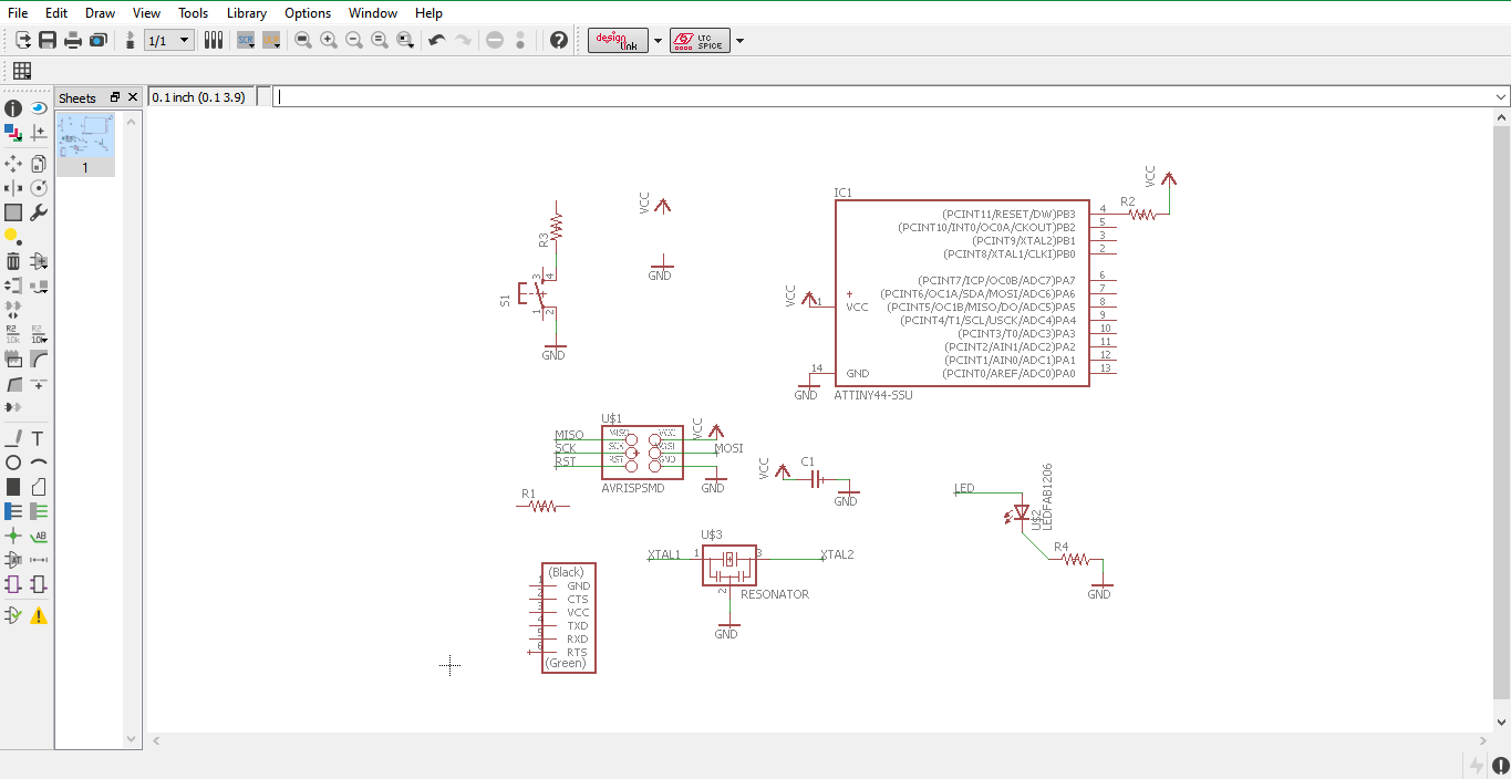
Step 4: Schematic
Once I was done adding all the relevant components, I connected all the relevant connections by using a schematic component called net label.
If two or more pins are attached to a net label with the same name, then they are considered connected by eagle. By using this feature, I made all the connections and now the schematic was complete.
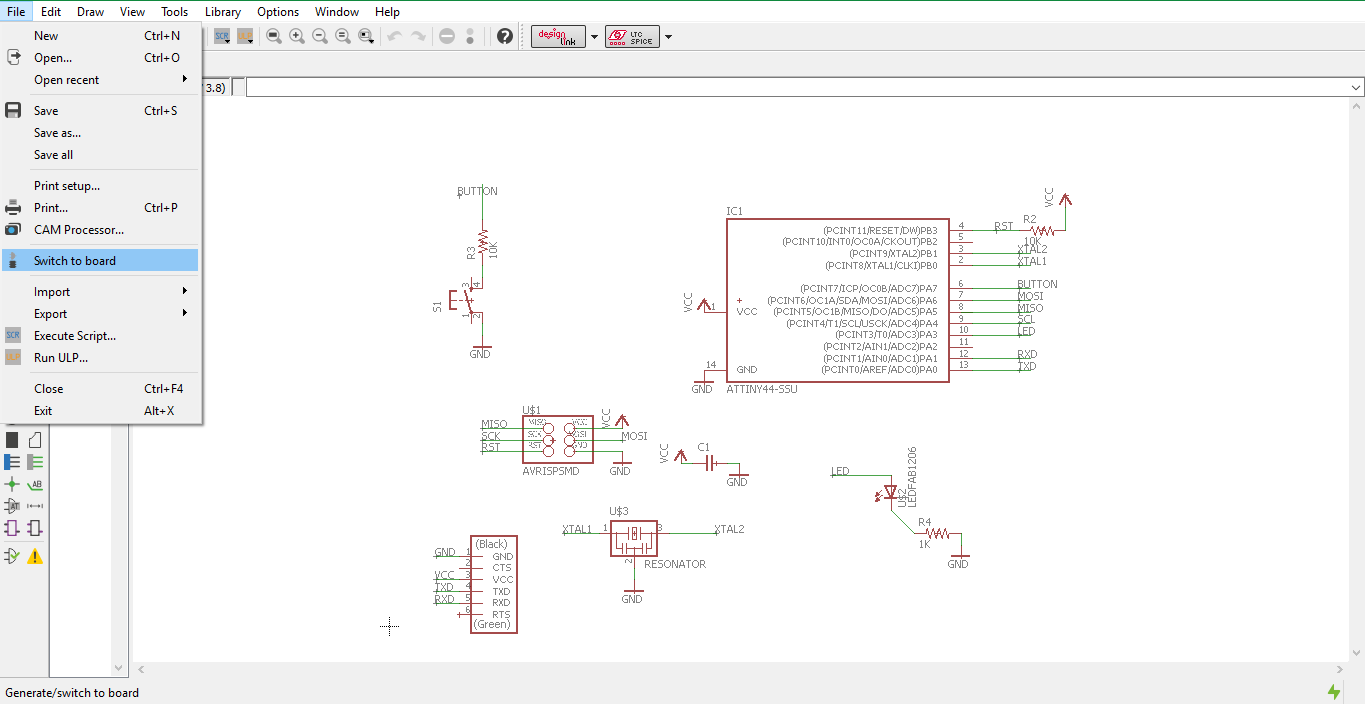
Step 5: Switch to board
After the schematic of the circuit was done and checked with ERC, I proceeded towards the board layout. I did this by going to File > Switch to Board. There is a “switch to board” icon.
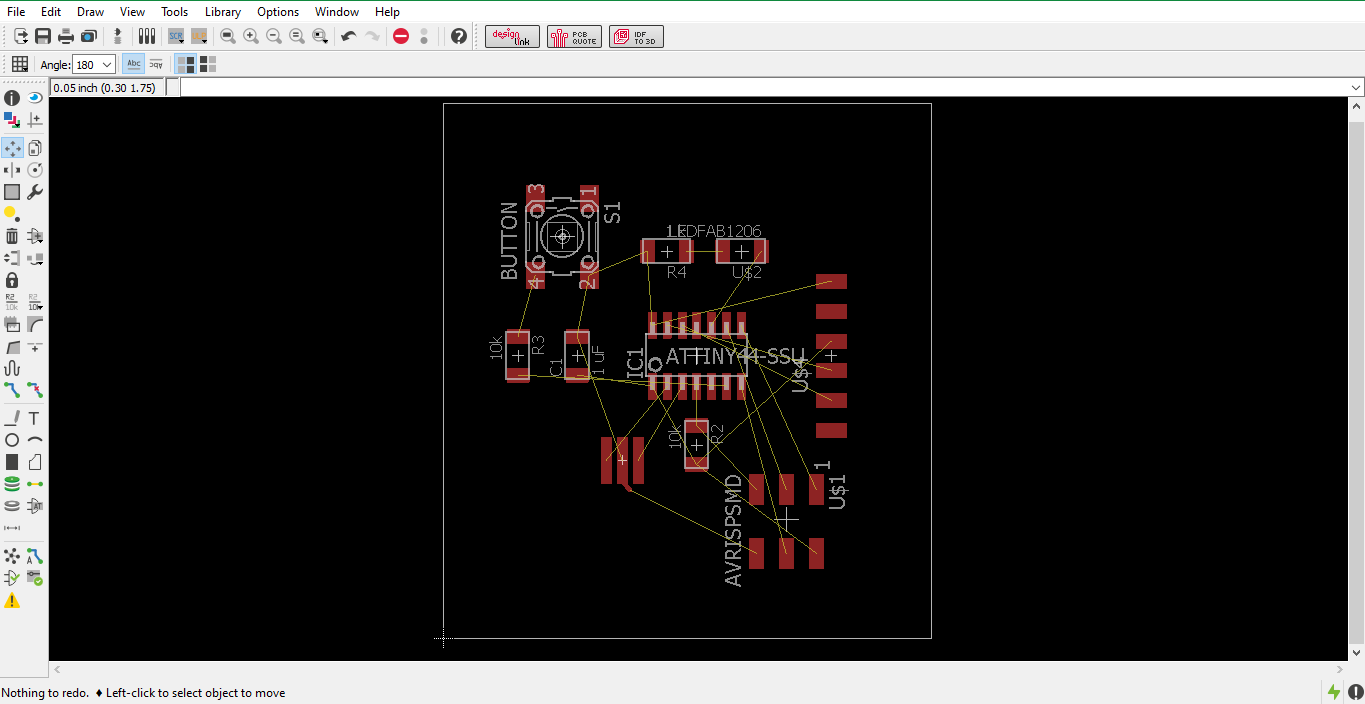
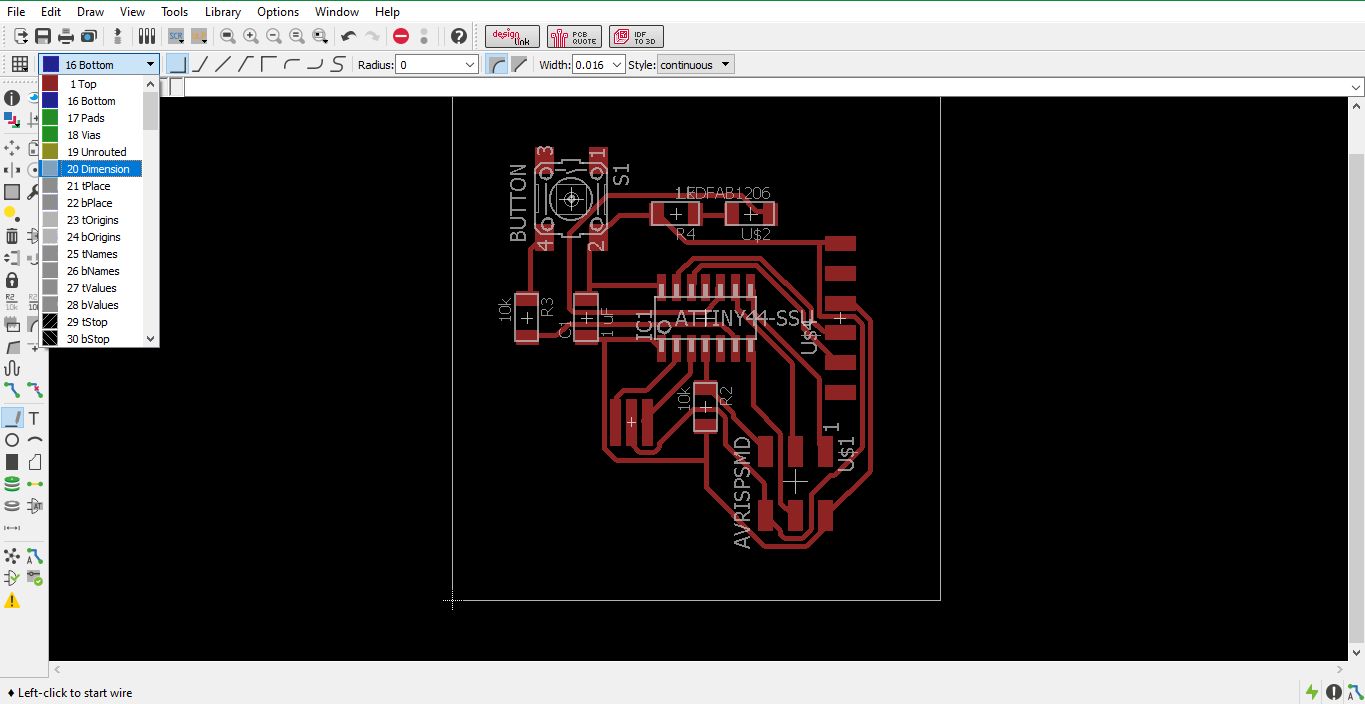
Step 6: Board layout created
This took me to another window which had the footprints of the schematic’s components along with a bunch of intersecting lines which are known as ratsnest. It is basically an indicator of the connections between the components. There was also a boundary indicating the size of the pcb.

Step 7: Arrange elements
I rearranged the components such that the AVRISP and the FTDI headers are not obstructed by any other component. One another mental rule I followed was to keep the ratsnest as little overlapping as possible. This increases number of results with no overlap during autorouting, which is a crucial future step. I also kept a decent amount of pcb around the components, again to ensure better auto-routing.
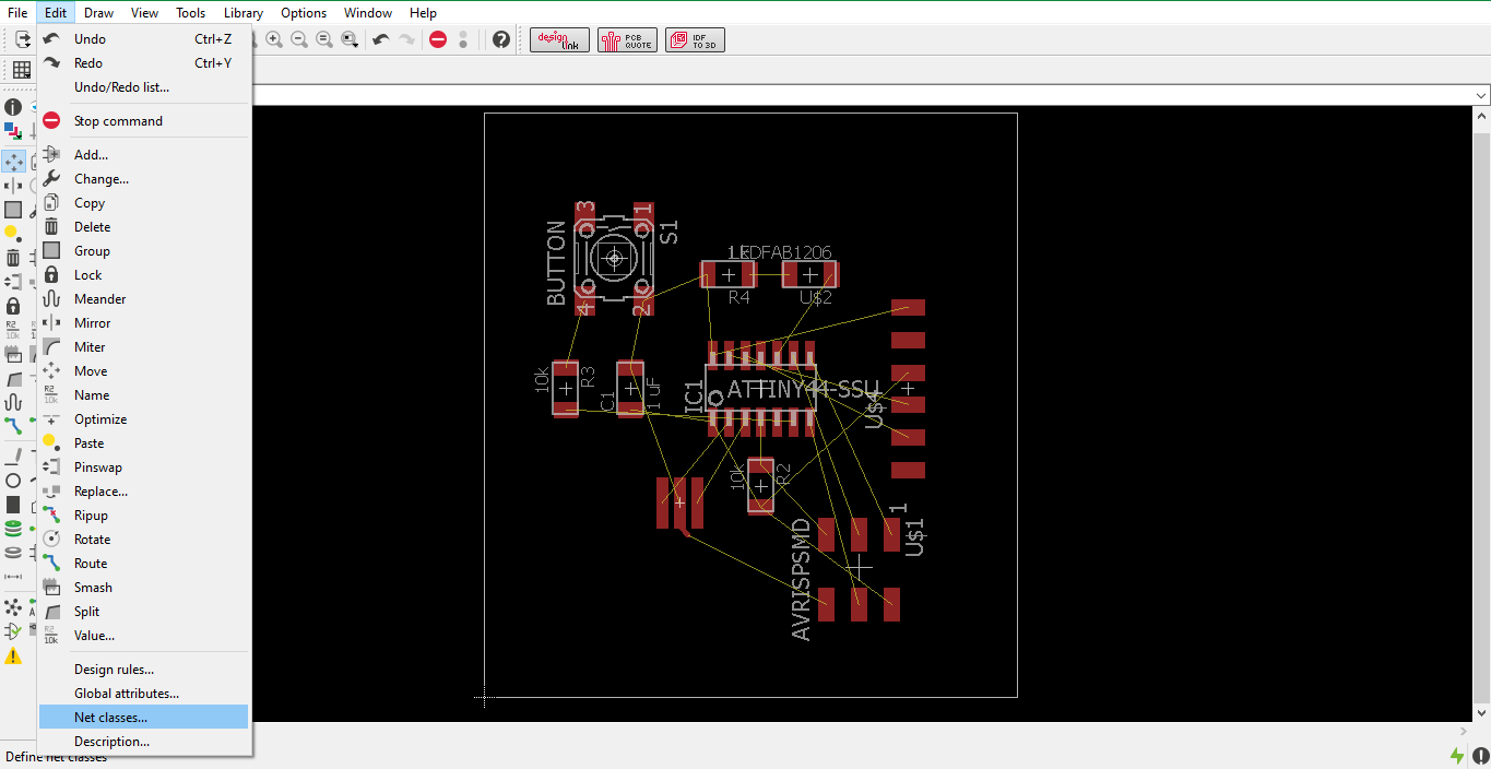
Step 8: Select net classes
Before I began auto-routing, I edited the net classes i.e. settings regarding the desired minimum width of traces, the minimum clearance between two traces etc. For that, I navigated to Edit > Net classes…
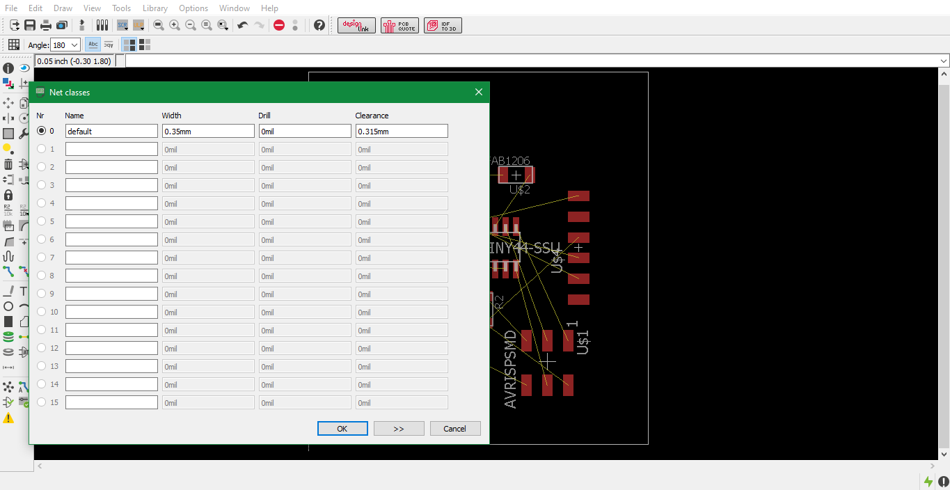
Step 9: Edit net classes
The settings that I chose are:
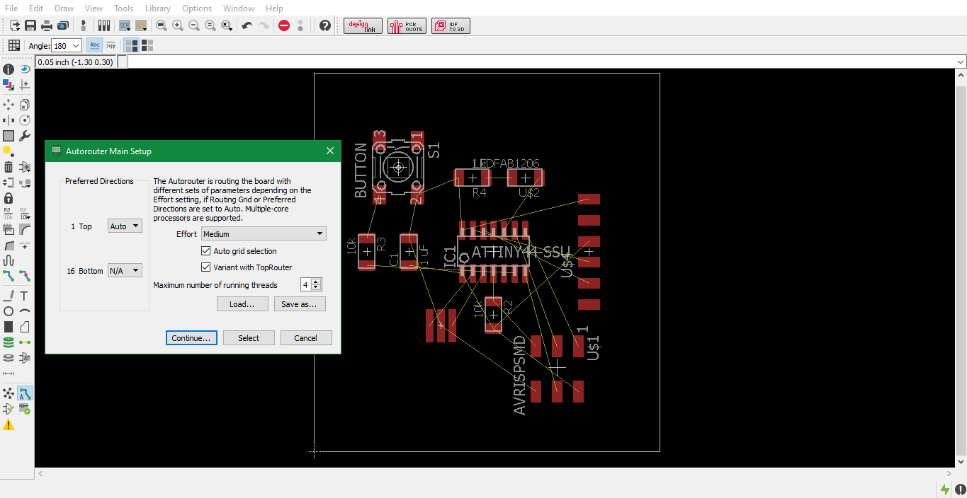
Step 10: Autoroute beginning
After clicking OK, I continued on to initiate autorouting. This is done by clicking on the relevant icon in the left vertical menu. Following are the setting I used:
And the rest are the defaults.
Step 11: Autoroute window
After that I clicked continue, which opened another window, showing progress of the routed paths per trial. It can design PCB traces from scratch or add to existing but incomplete traces. As soon as I hit Start, the computer starts running trials for design, optimising PCB size, trace width, clearance, overall area of the traces, etc.
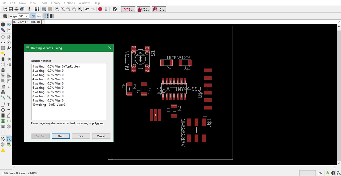
Step 12: Autoroute results
I chose the design that was produced by the TopRouter, simply because it had the least area consumed and was densely packed.
Step 13: DRC check window
After that I ran a DRC or Design Rules Check. This is done by clicking on the DRC icon in the left vertical toolbar. This opens another window that allows you to load a .dru file, which basically contains presets for design rules.
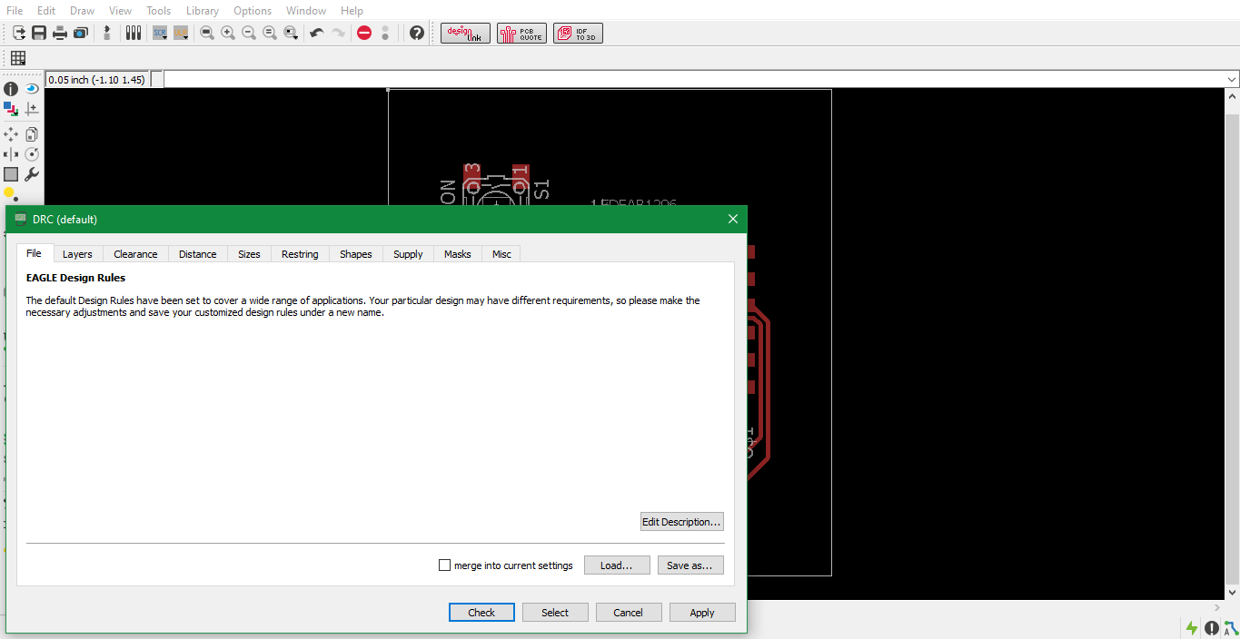
Step 14: DRC settings loaded
I loaded the official fabacademy dru file which is given in the common folder along with the other files for the same week. After loading it, I clicked on Check, and the result was error-free, so I moved onto the next step.

Step 15: Drawing interior
I selected Wire from the left vertical toolbar, and in the drop-down menu below edit, I selected Dimension and then proceeded to draw a boundary around the board traces. This will be my interior file.
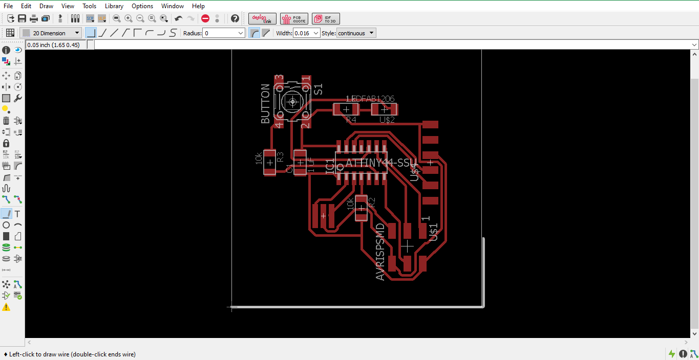
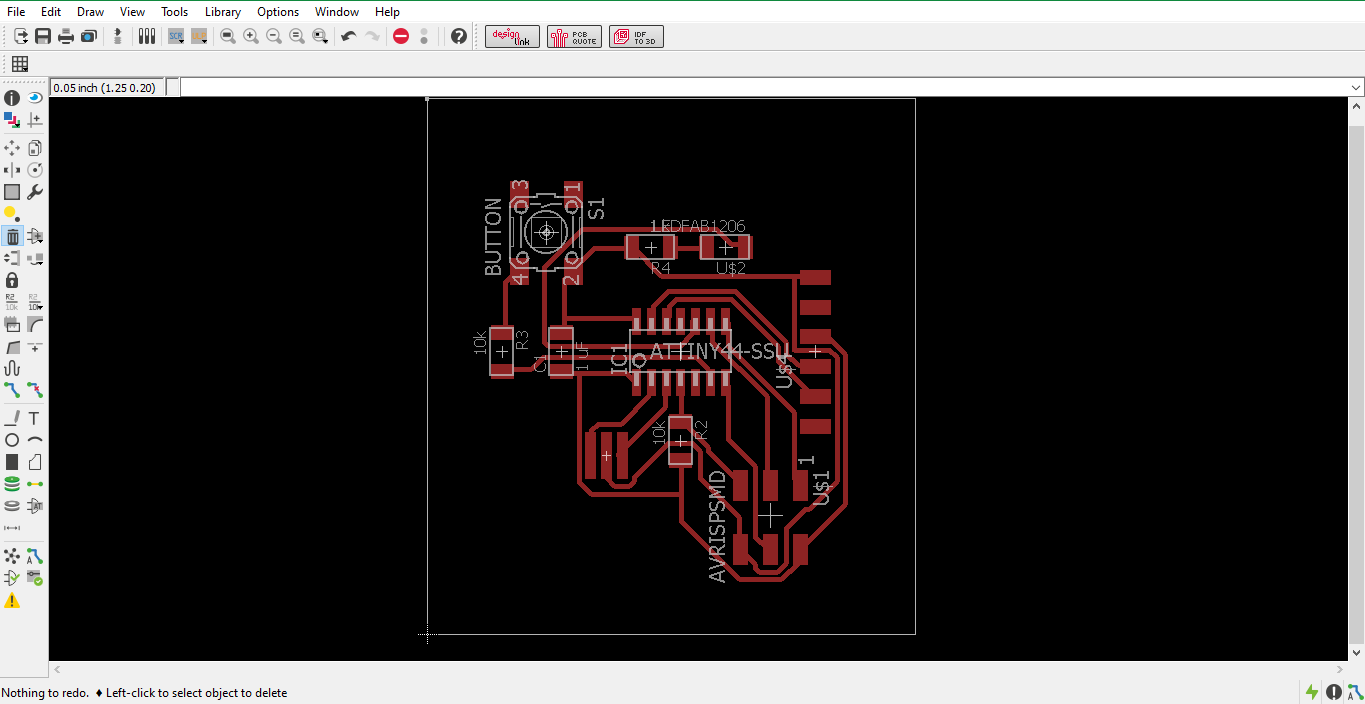
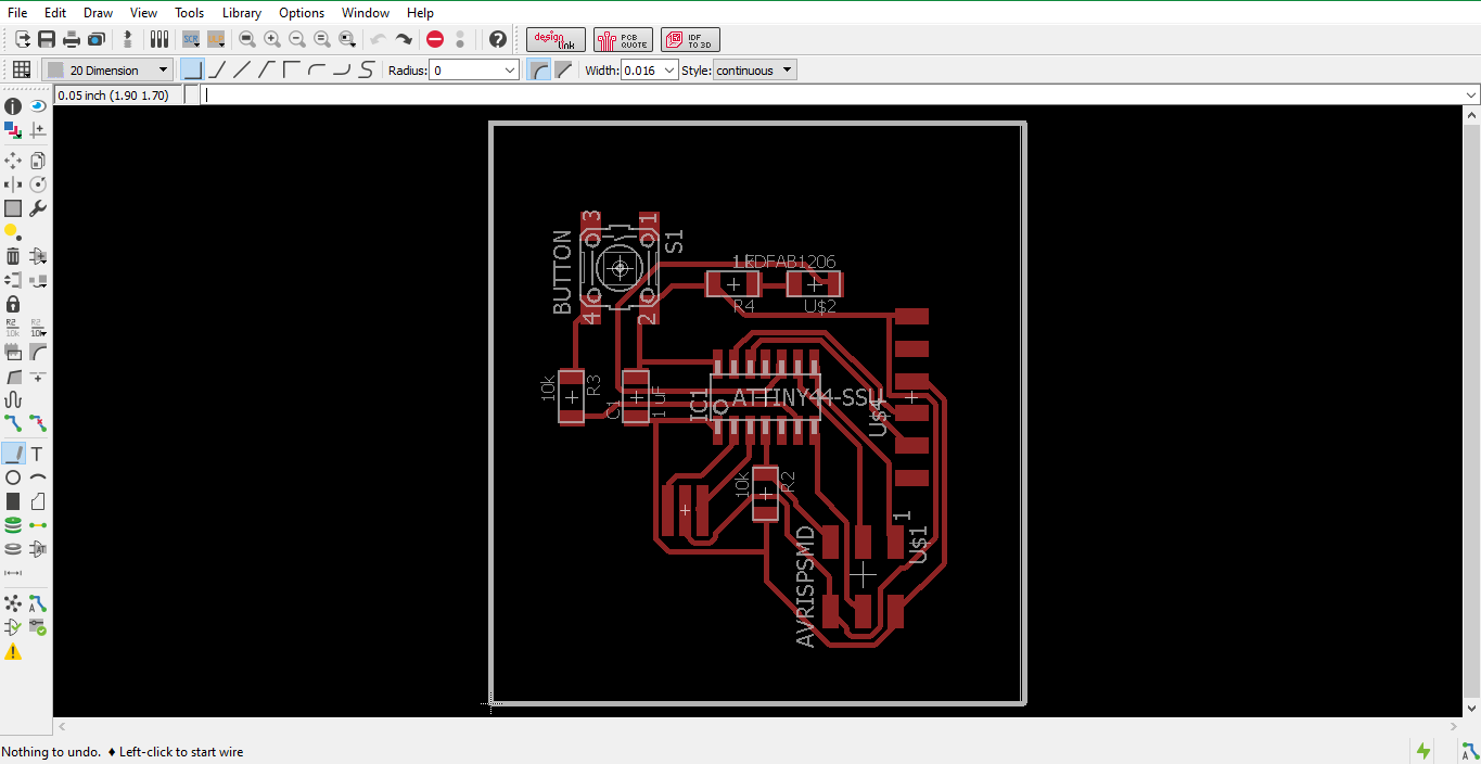
Step 16: Finished board
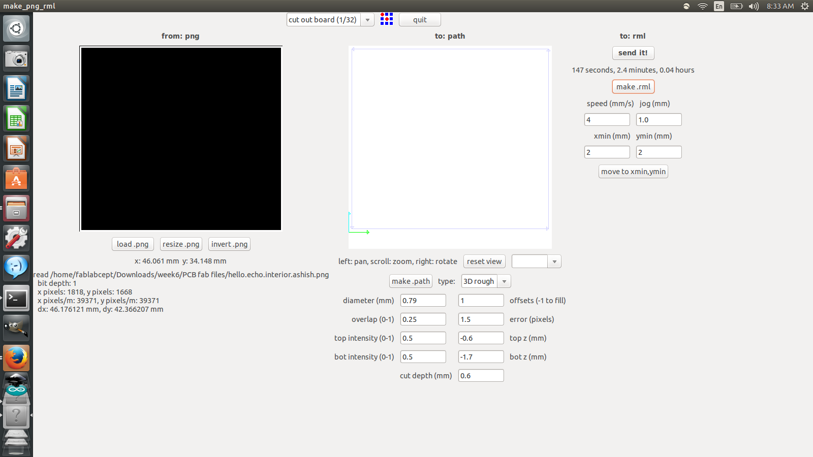
This is the finished board, now the files can be generated for pcb milling.
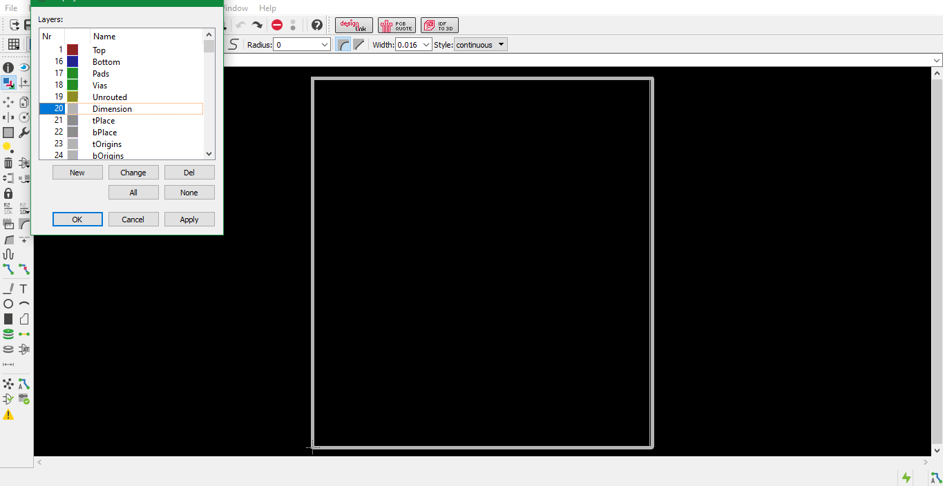
Step 17: Layer settings
For generating PCB Fab files, I had to generate files layer by layer. To do that, I navigate to View > Layer settings…
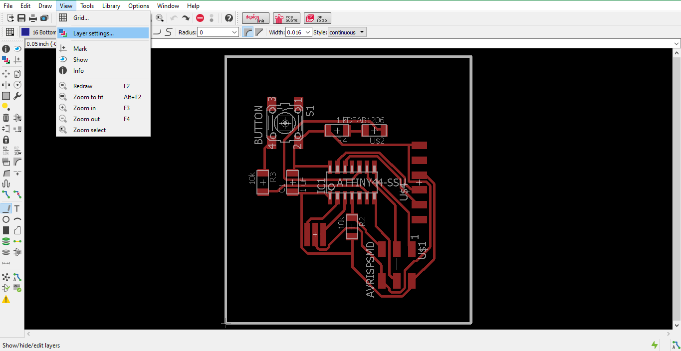
Step 18: Layer settings window
A new window appears, listing all the layers. Layers can be turned on and off, depending upon the requirement.
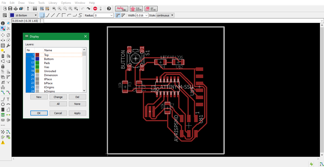
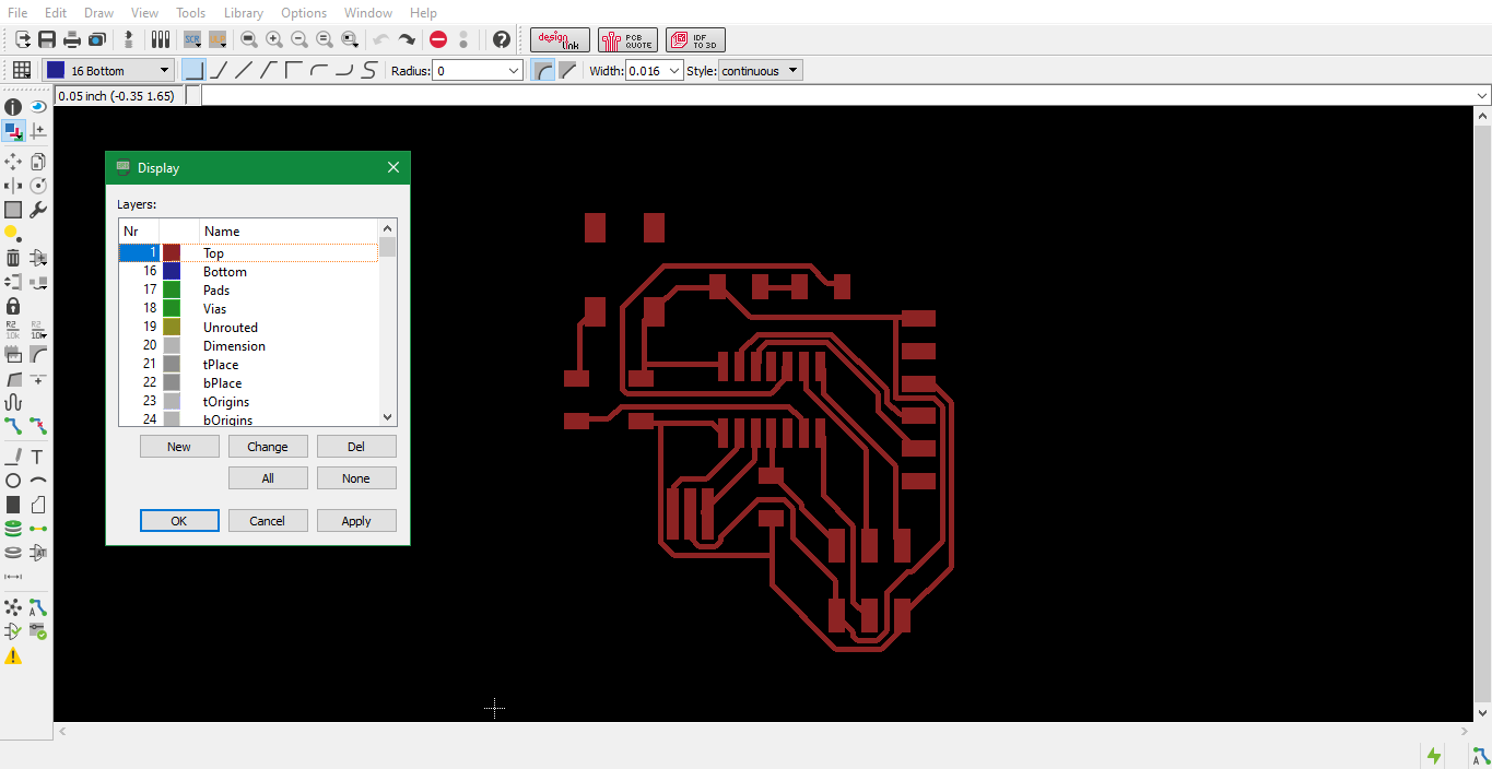
Step 19: Showing traces
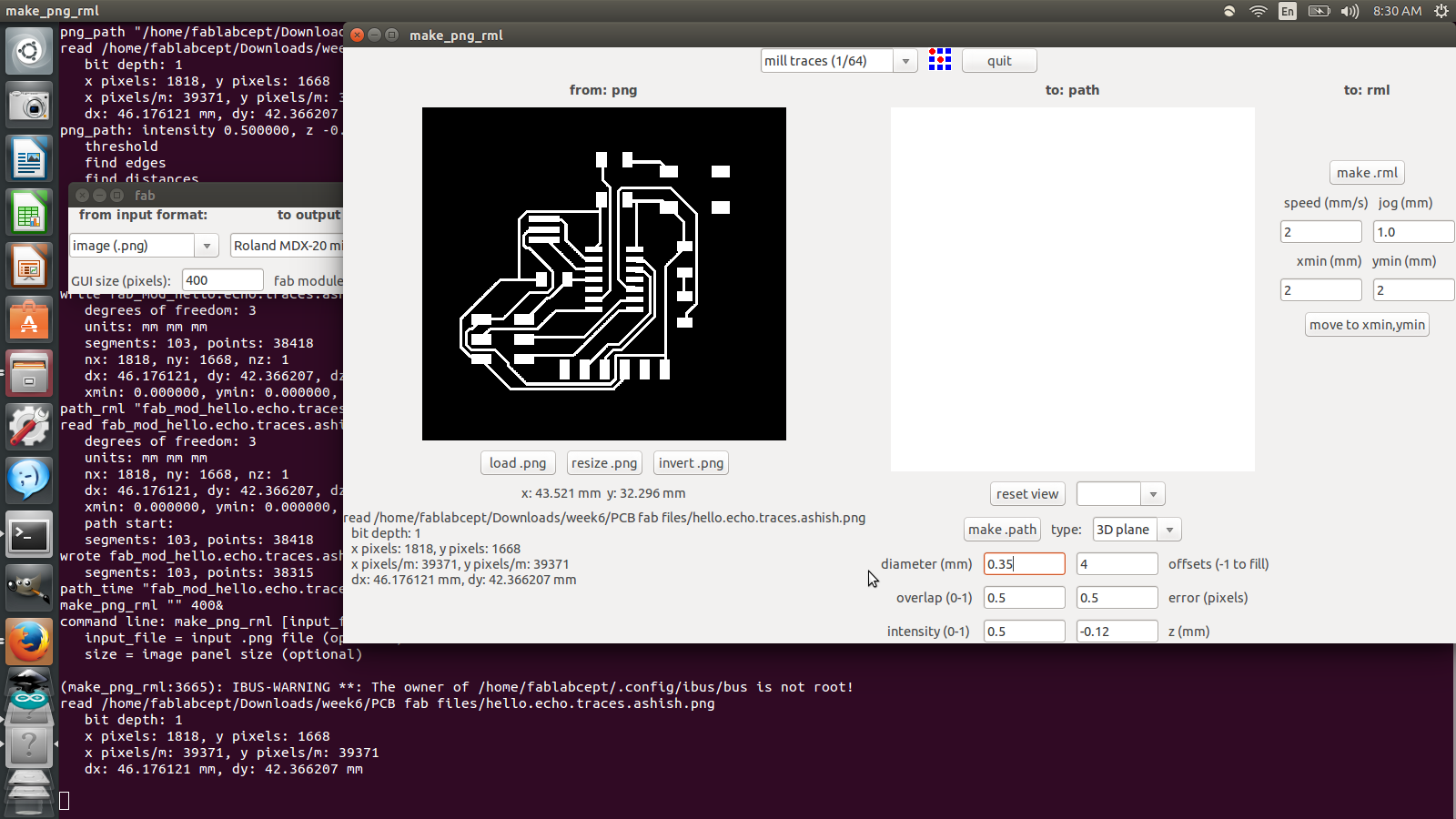
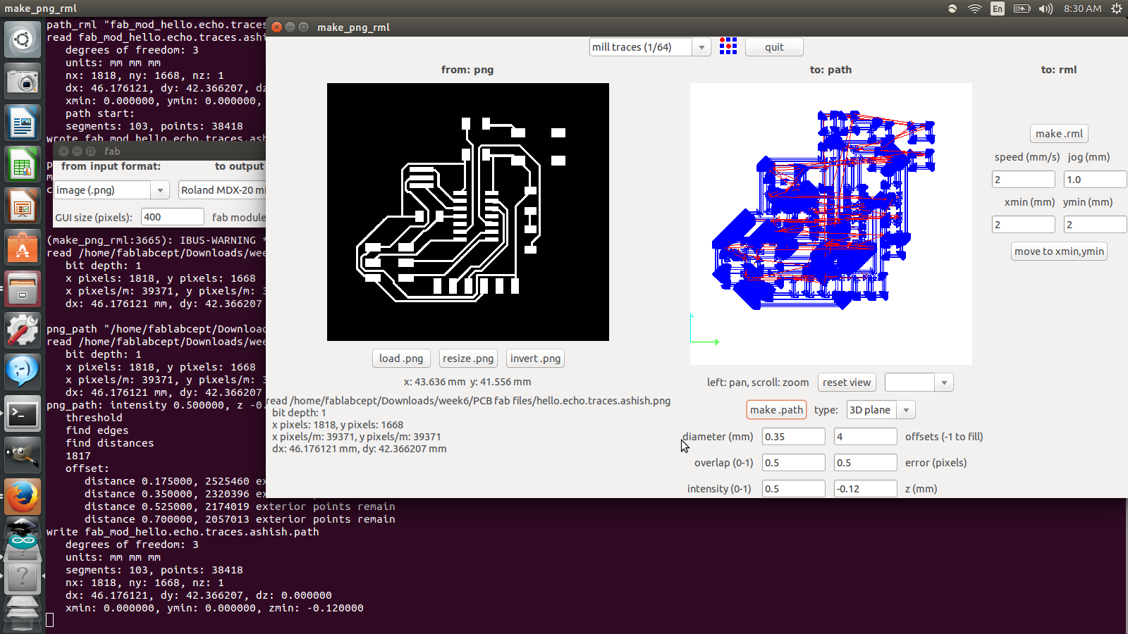
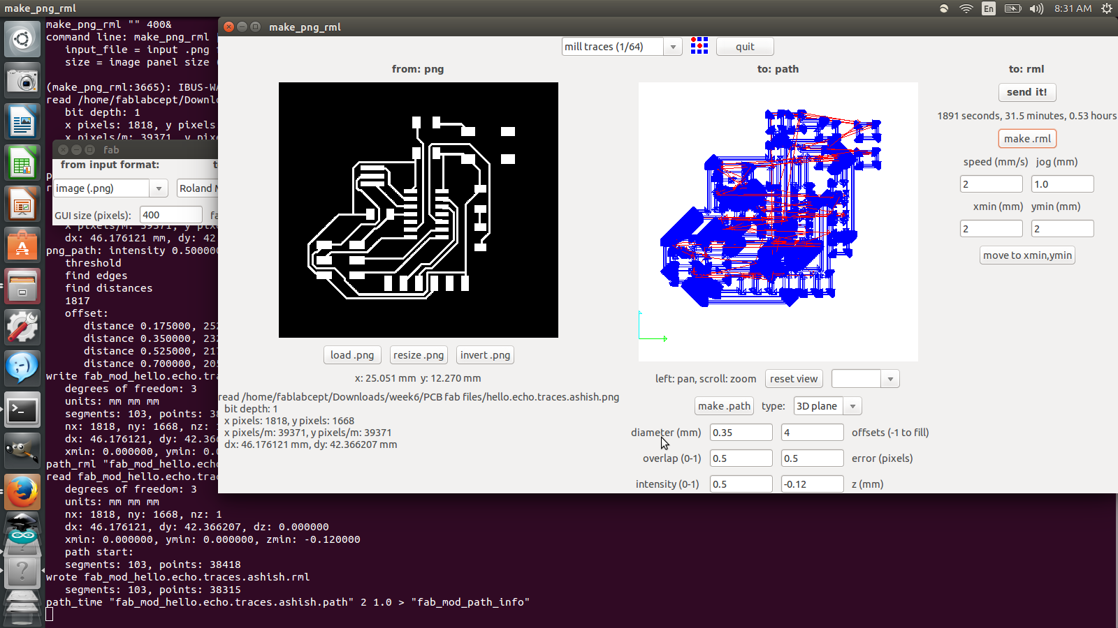
First I decided to export the traces as a png file. For that, I turned all the layers off by clicking on None. Then I selected Top. This will select all the portions marked by red, including the traces and the footprints of the components.
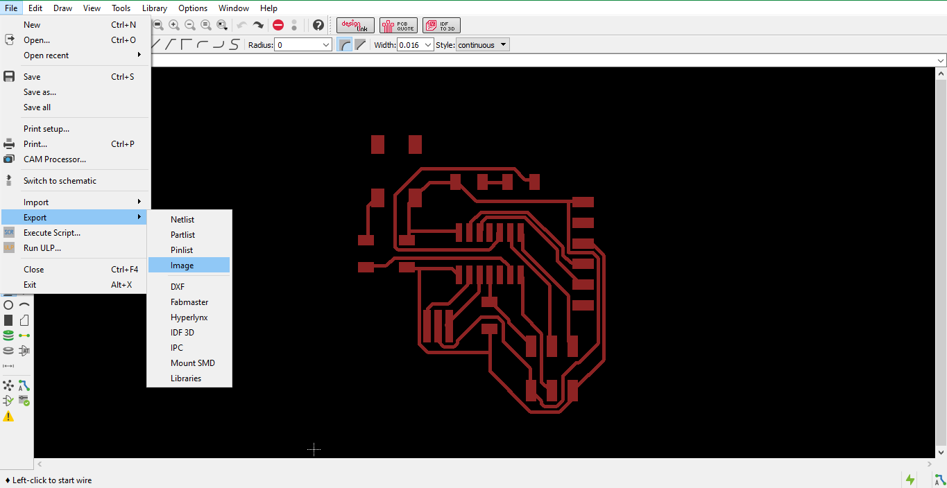
Step 20: Exporting as image
Now, to export this layer as an image, I navigated to File > Export > Image.
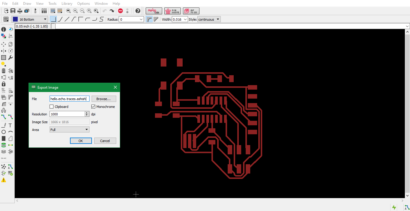
Step 21: Export window
This opens another window that allows me to export the image in png format to any desired location and desired resolution. I chose a resolution of 1000.
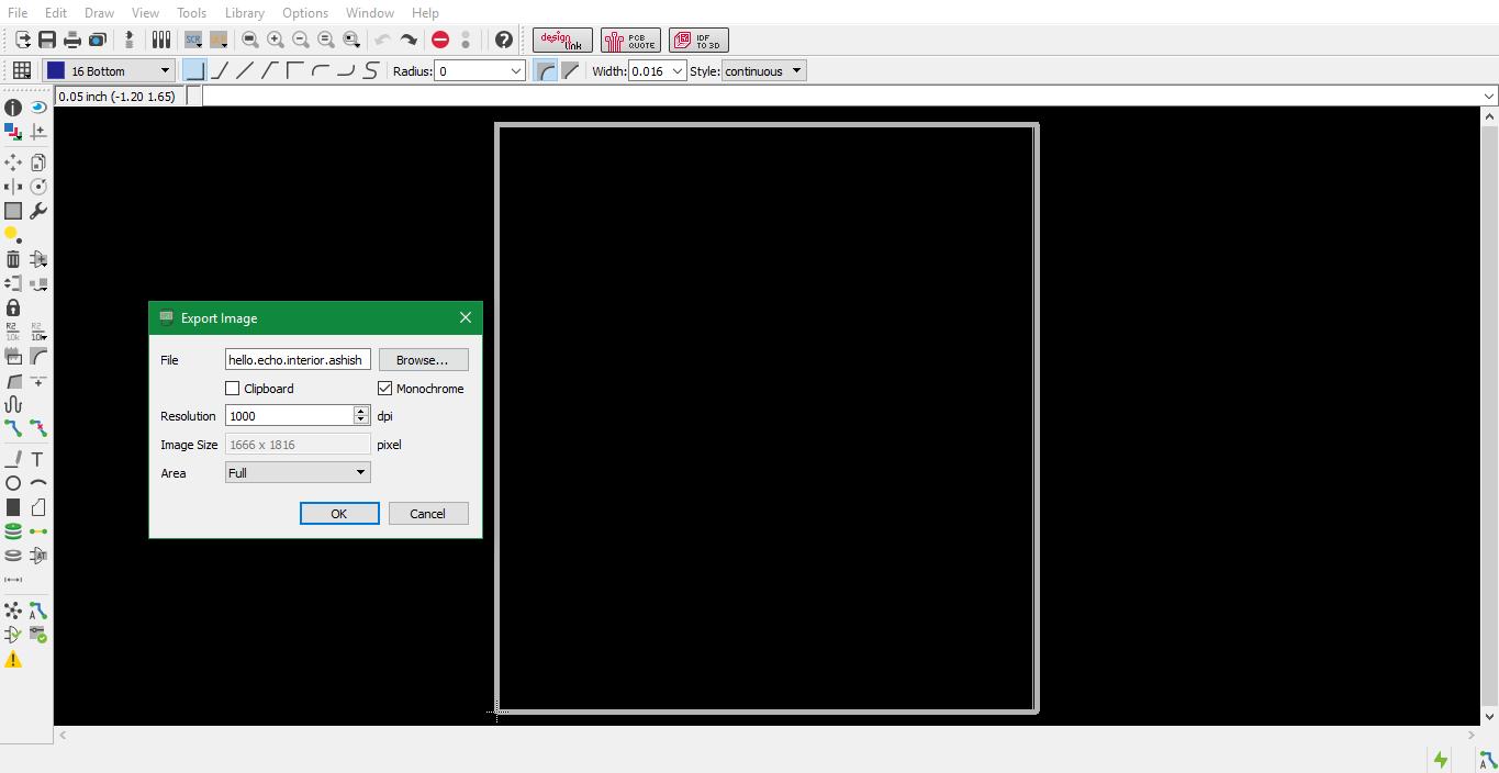
Step 22: Showing dimension
After saving the traces file, I reopened the layer setting and deselected Top and selected Dimension. This selects the boundary of the PCB
Step 23: Export window
So I repeated steps 20 and 21 and exported the file for cutting out the interior of the pcb.
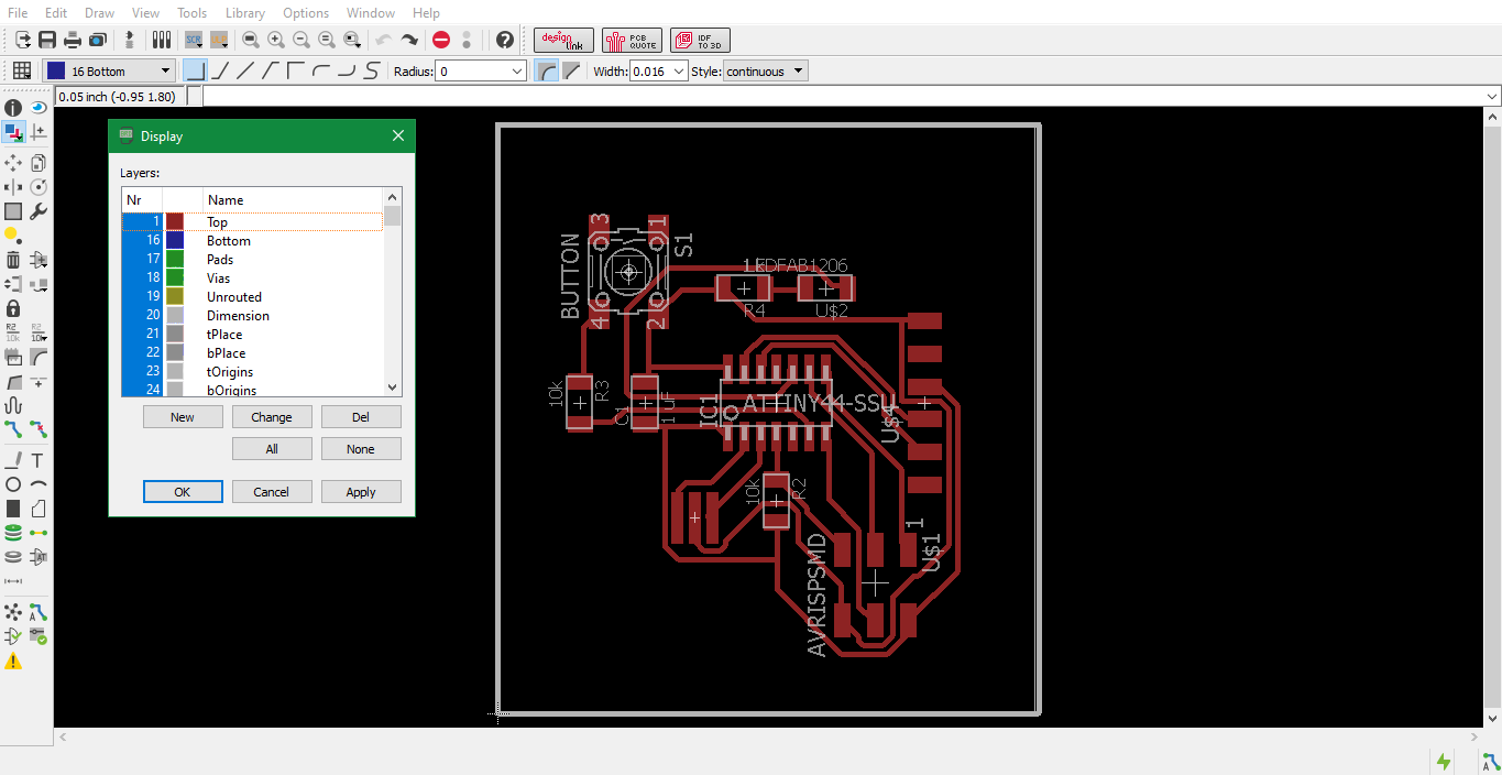
Step 24: Showing all details
And finally, I selected all the relevant layers that contained details such as the part names and values and also their physical footprint.
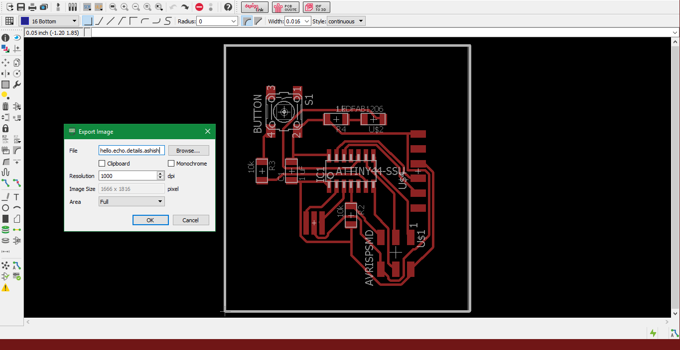
Step 25: Export window
Now I exported the image again using steps 20 and 21 and saved it for reference during the production of the board.
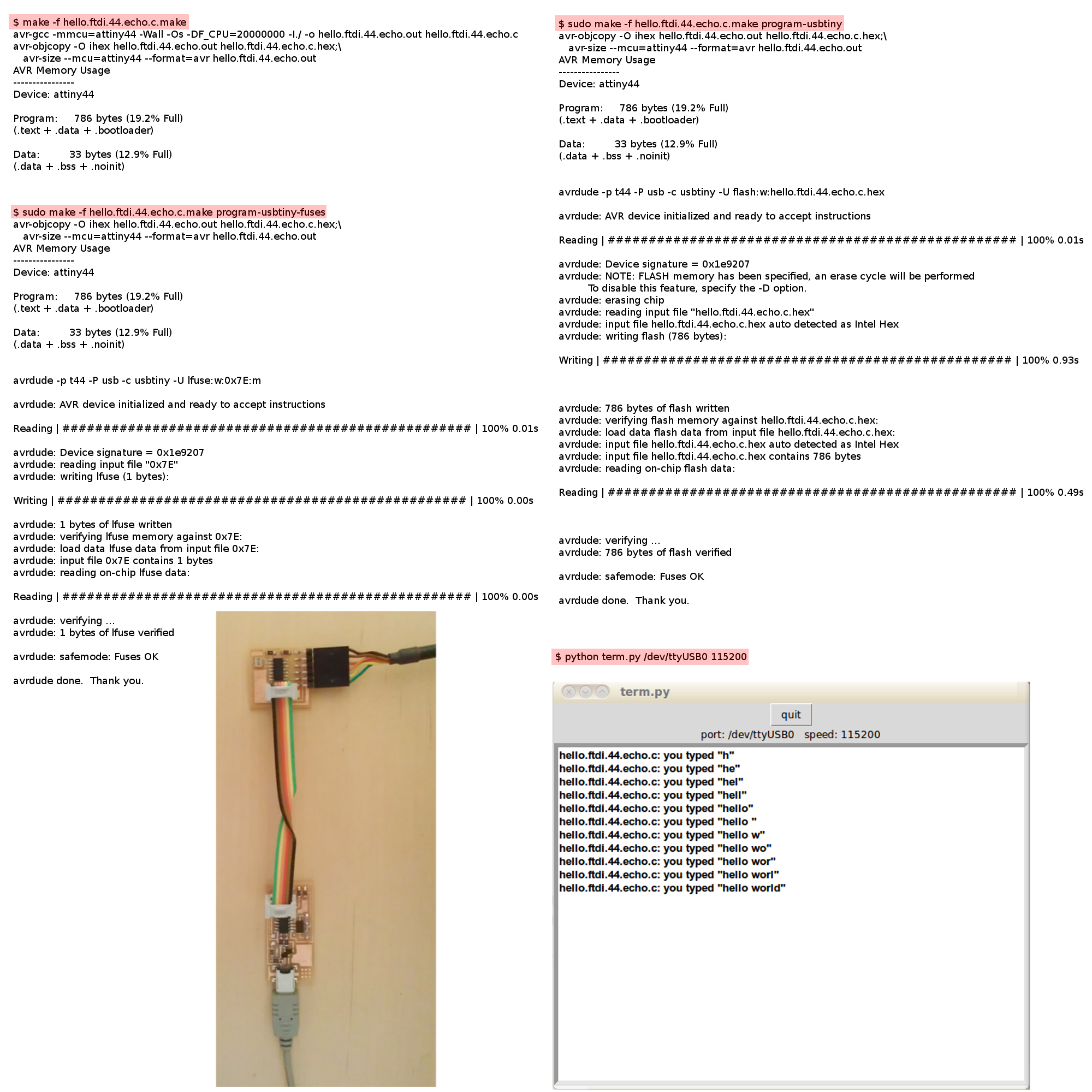
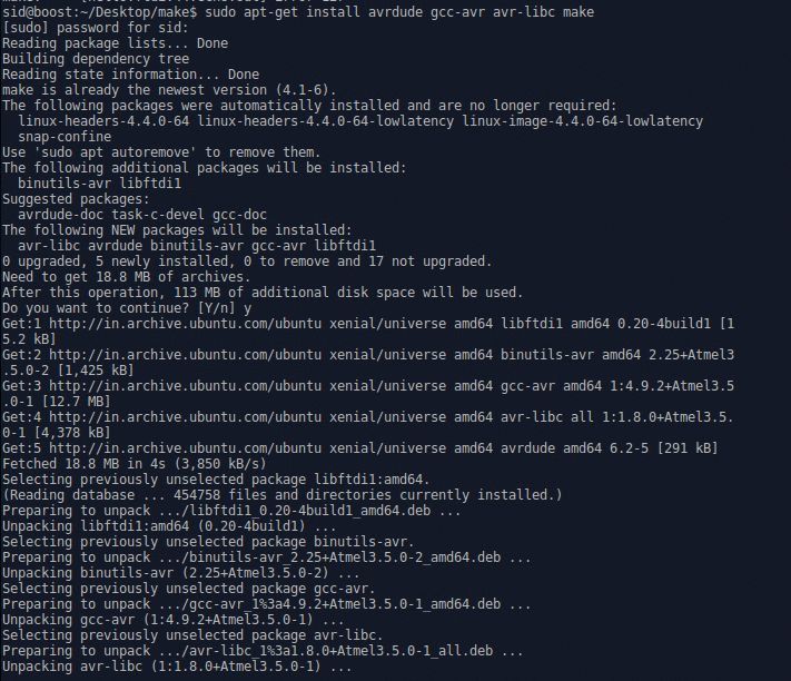
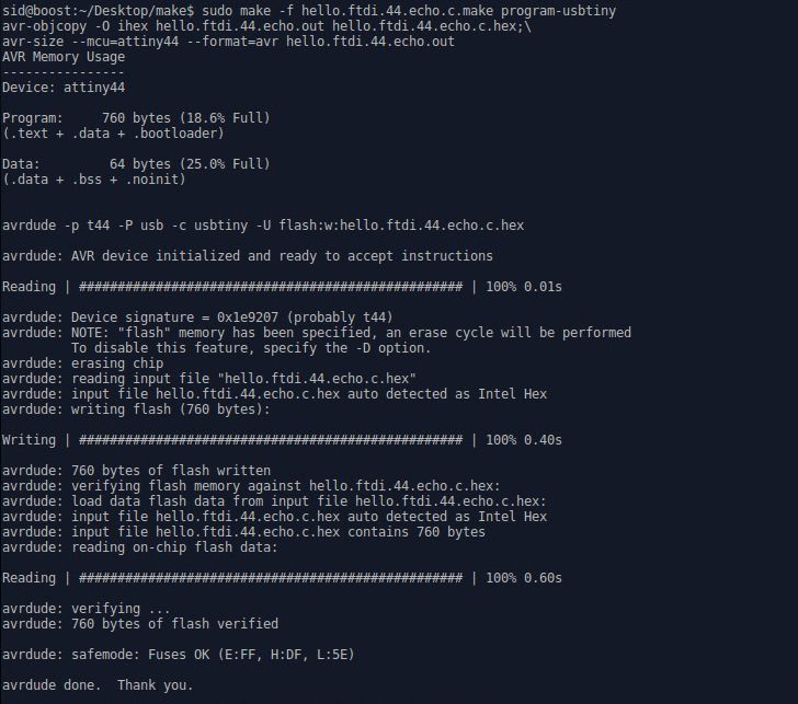
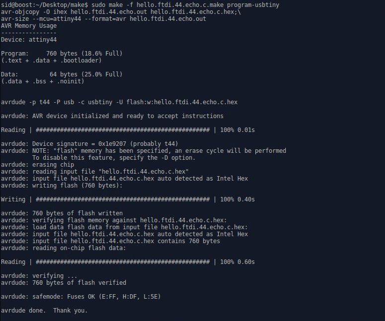
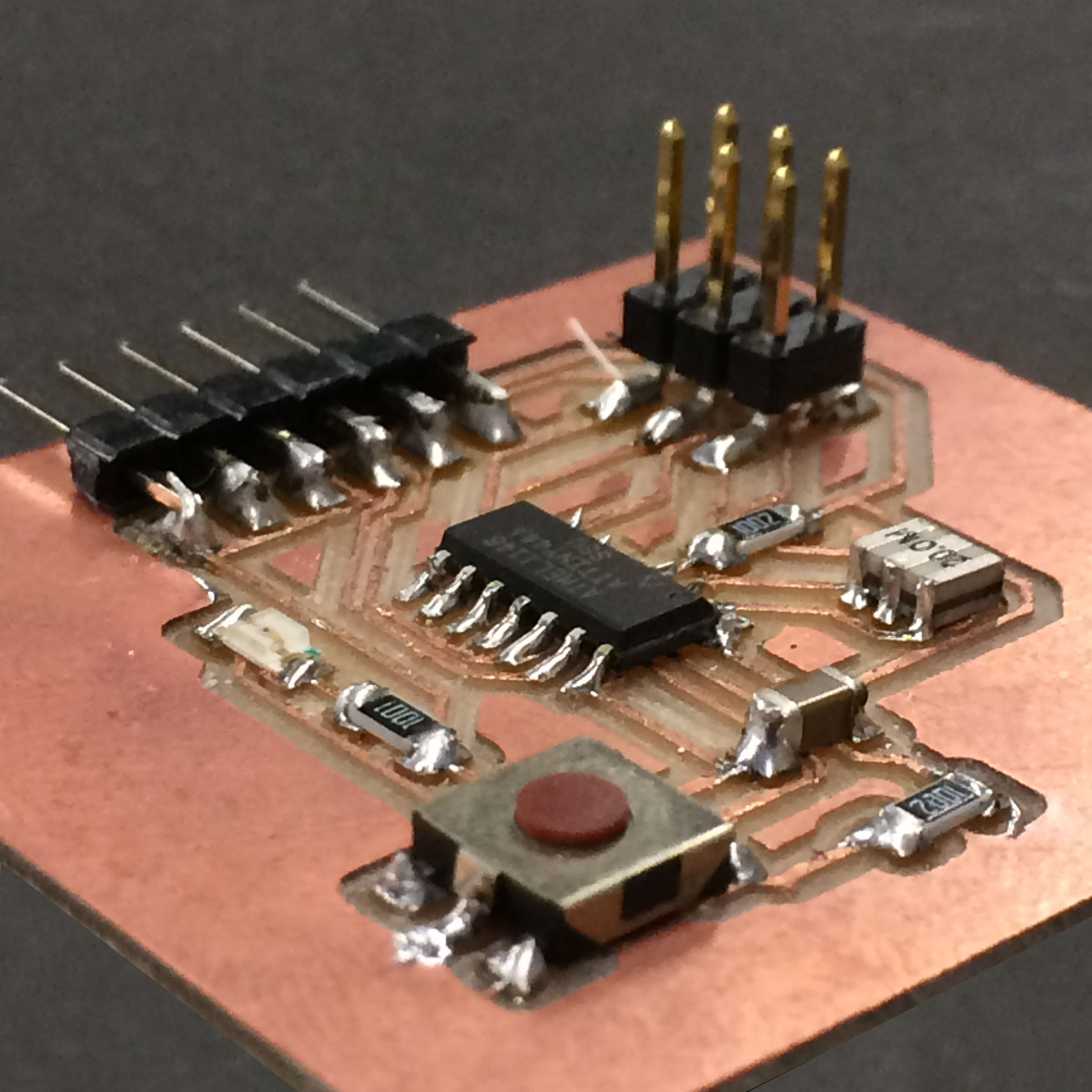
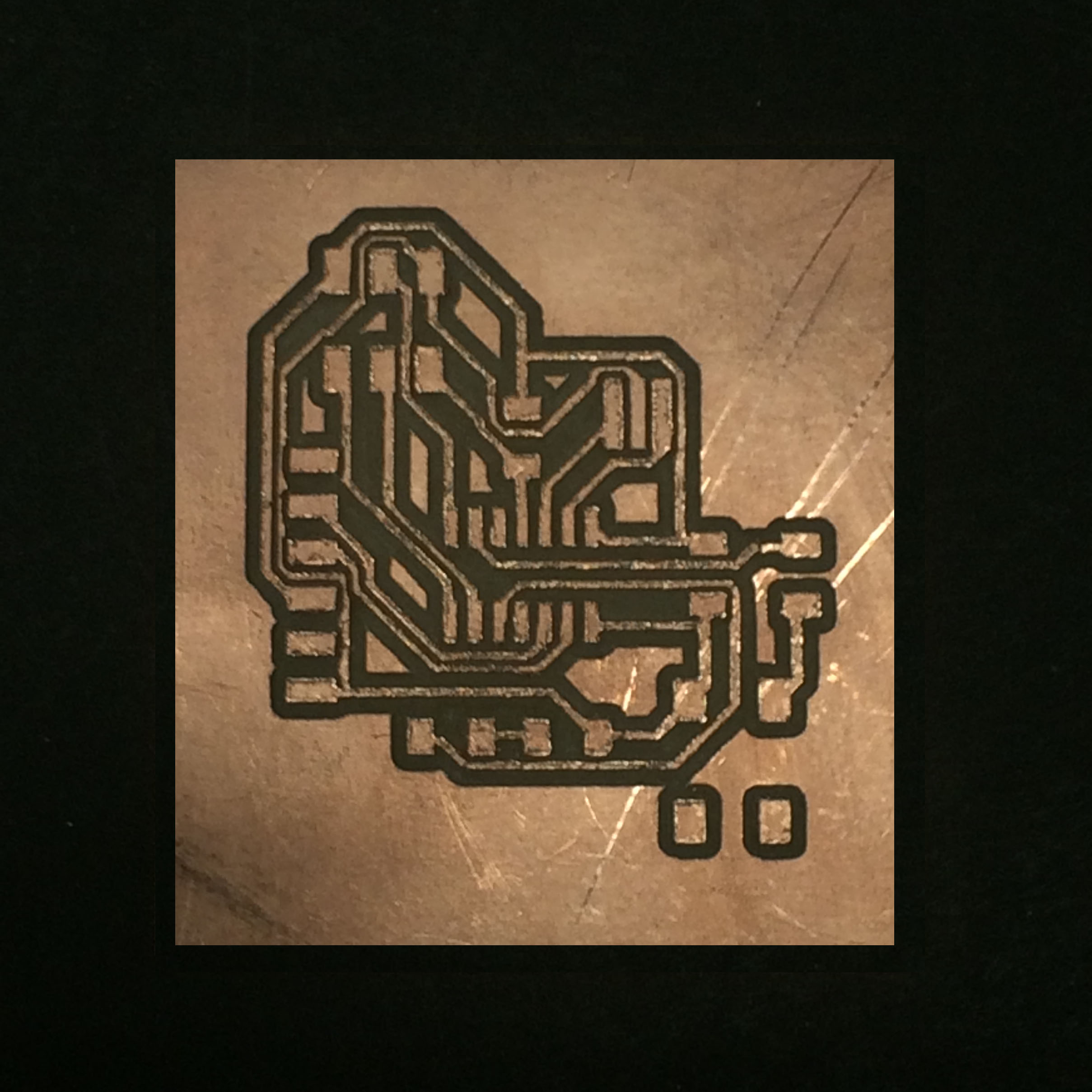
Circuit Board


Testing