- Week 15 +
networking and communications
Tasks
Introduction
For this week’s assignment, I have chosen Rx-Tx form of communication also known asynchronous bus communication. The reason I chose this form of communication was that I wanted to control individual servos in my final project. Another alternative method of communication would be I2C communication.
Here are the steps to create the node and bridge board for the circuit.
Designing the Bridge board
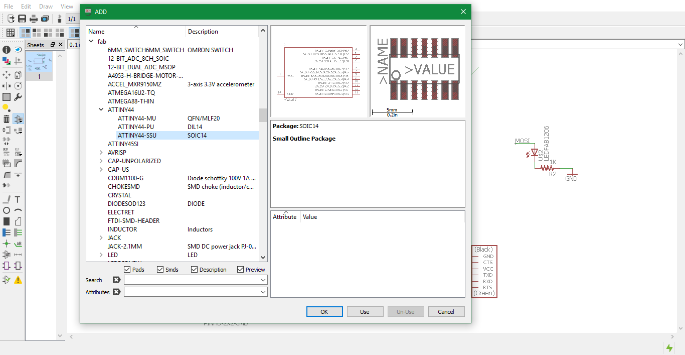
Step 1: Adding components to schematic
The series of steps is the same as previous weeks. I began with adding components to the schematic window.
Step 2: Schematic
After adding all the components and making the relevant connections, the schematic was complete.

Step 3: Switch to board
Once the schematic was complete, I navigated to File > Switch to board.

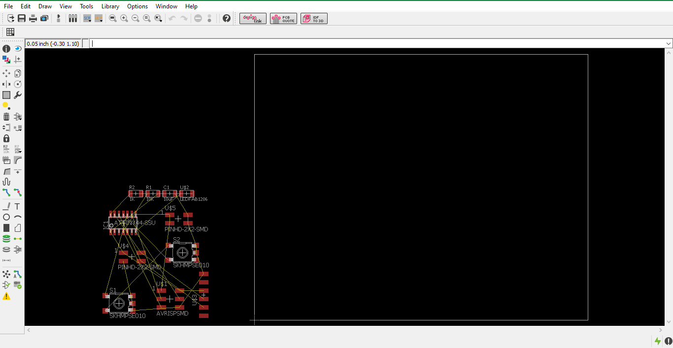
Step 4: Begin board layout
The Board Layout window was created, where all the components with their connections in ratsnest form are given.
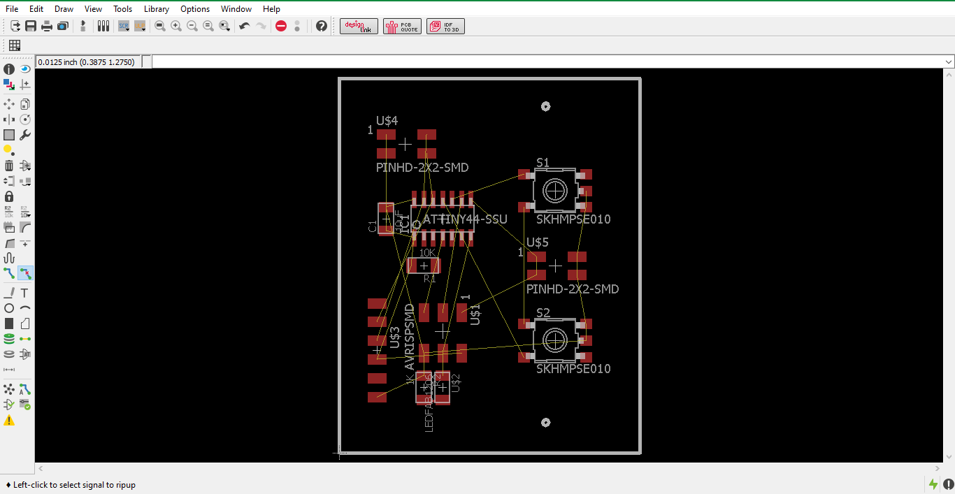
Step 5: Components arranged
I rearranged the components according to my requirements and resized the PCB. I also made the interior of the board.
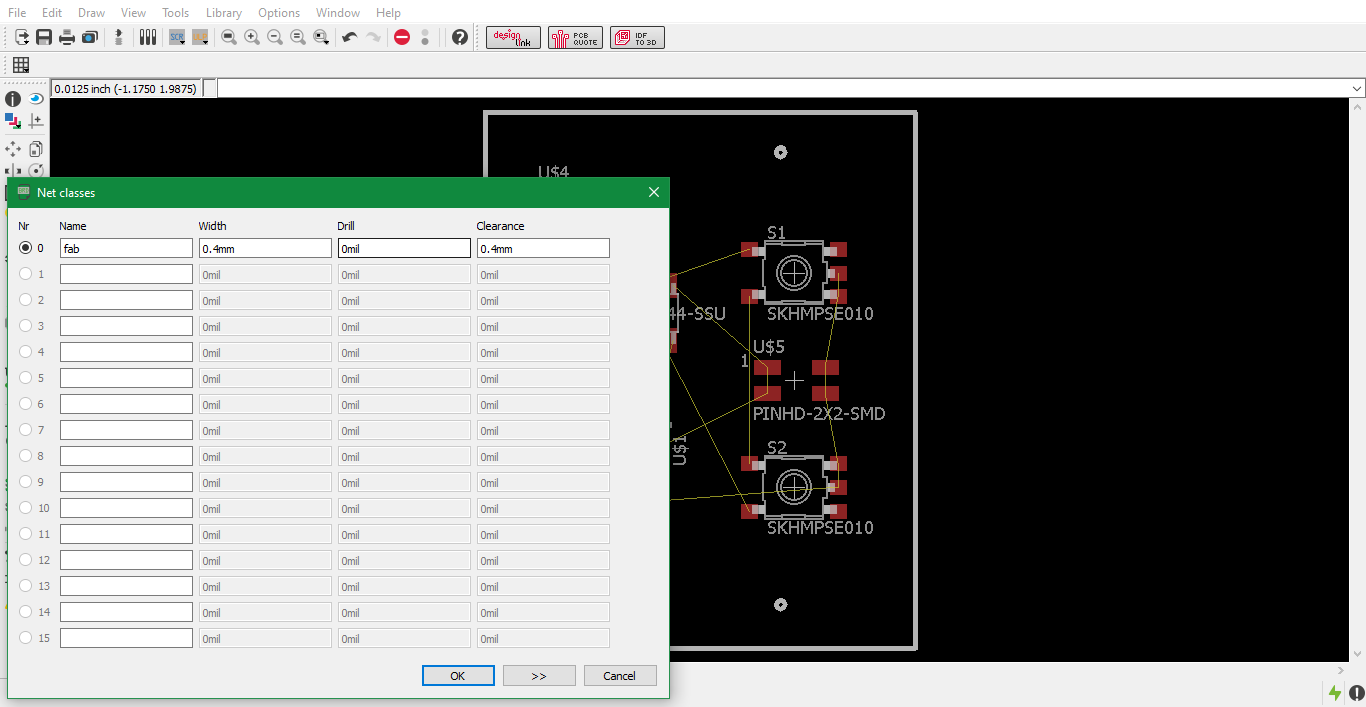
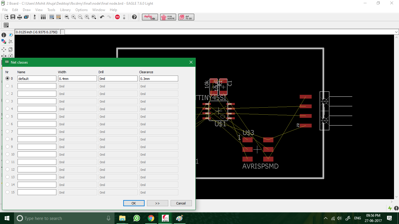
Step 6: Net classes
After that I edited the net classes to with the following settings:
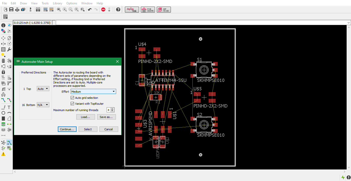
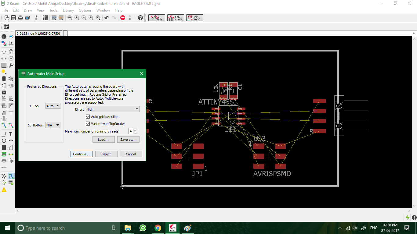
Step 7: Autorouting begins
Once the net classes are chosen, I began autorouting with the following settings:
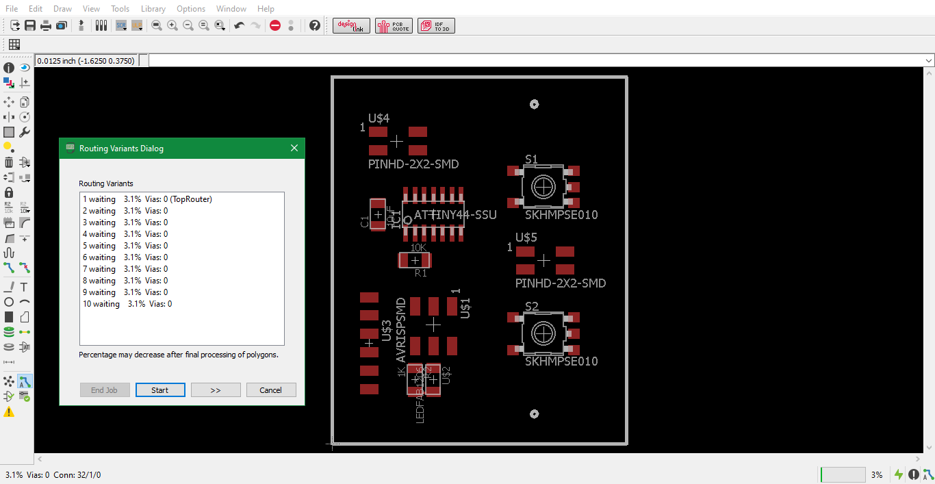
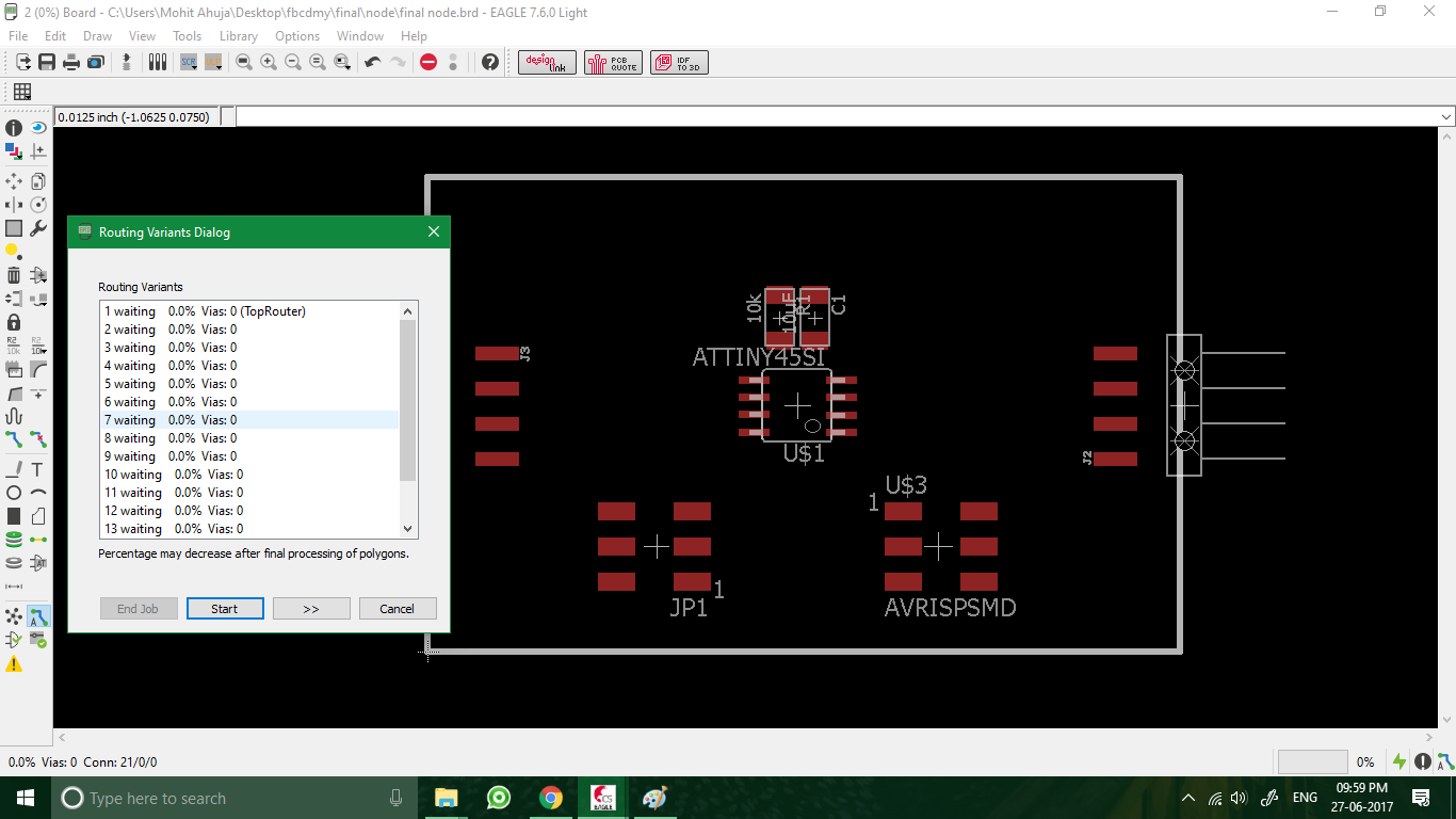
Step 8: Autorouting window
Autorouting window showing the running threads for different designs
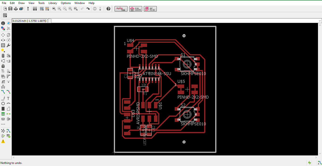
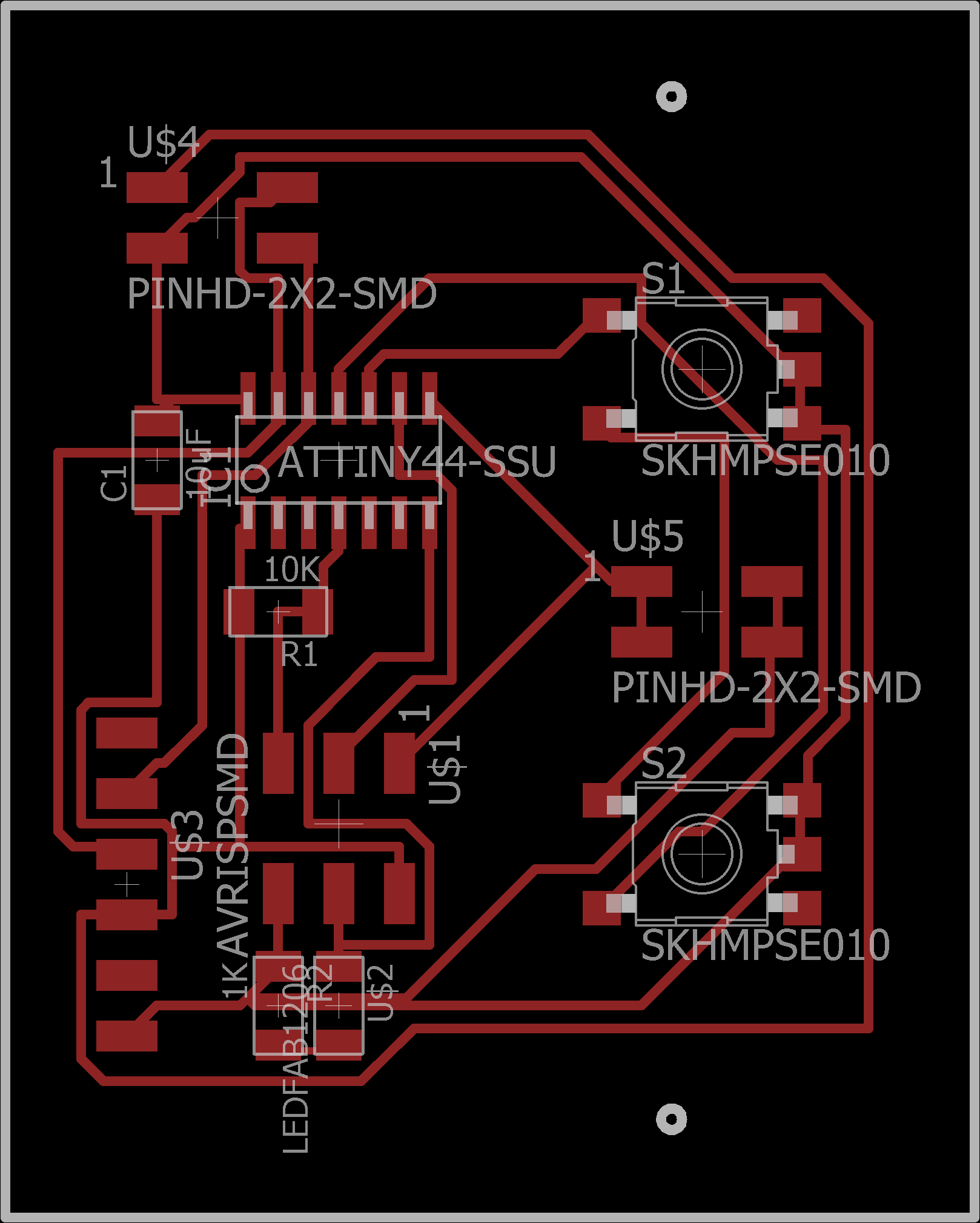
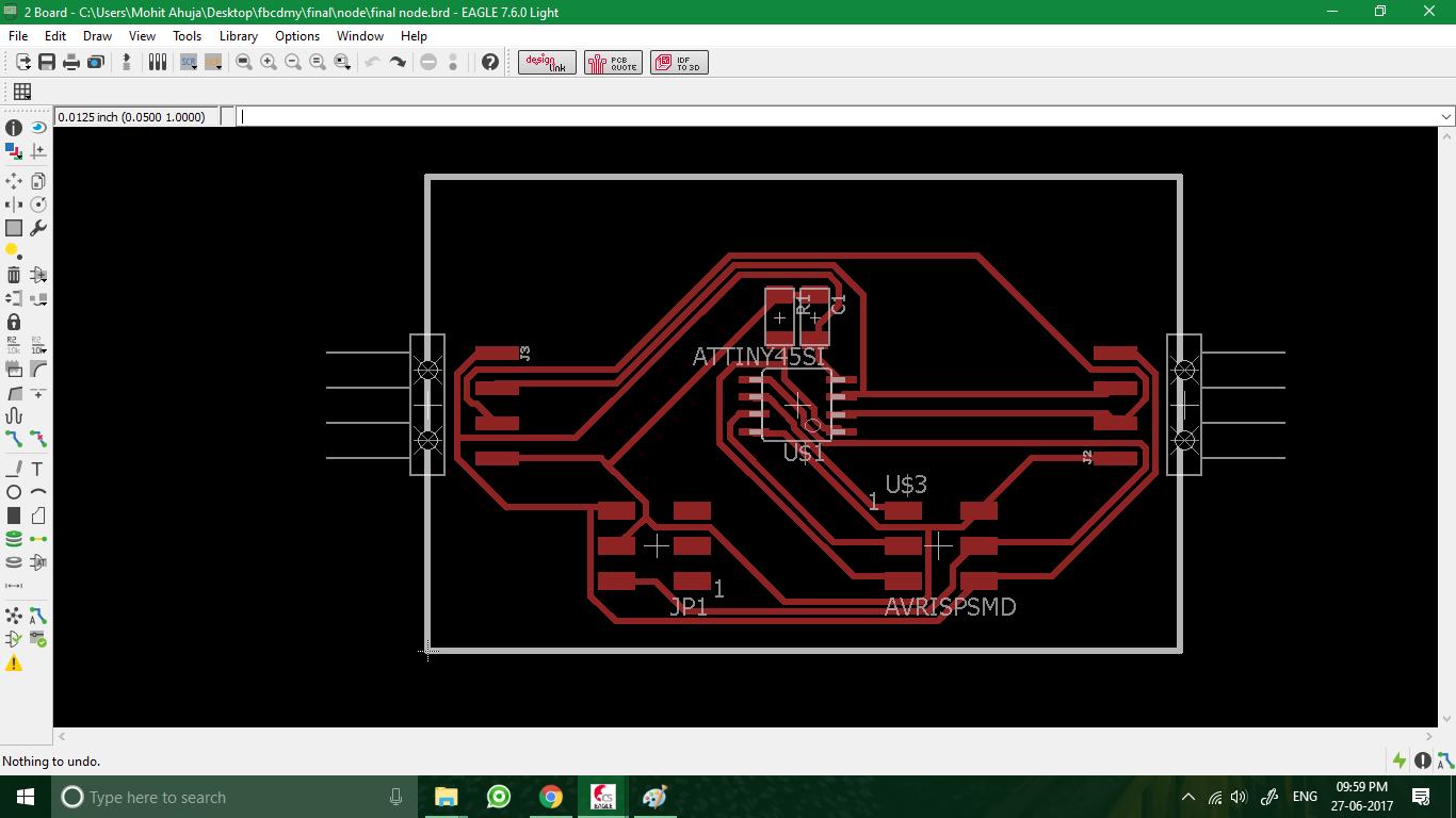
Step 9: Routing complete
The best possible design was chosen for the PCB and the circuit design was checked with DRC to reveal no errors.
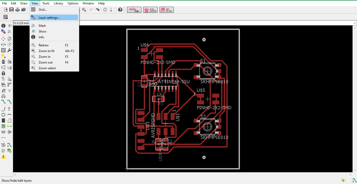
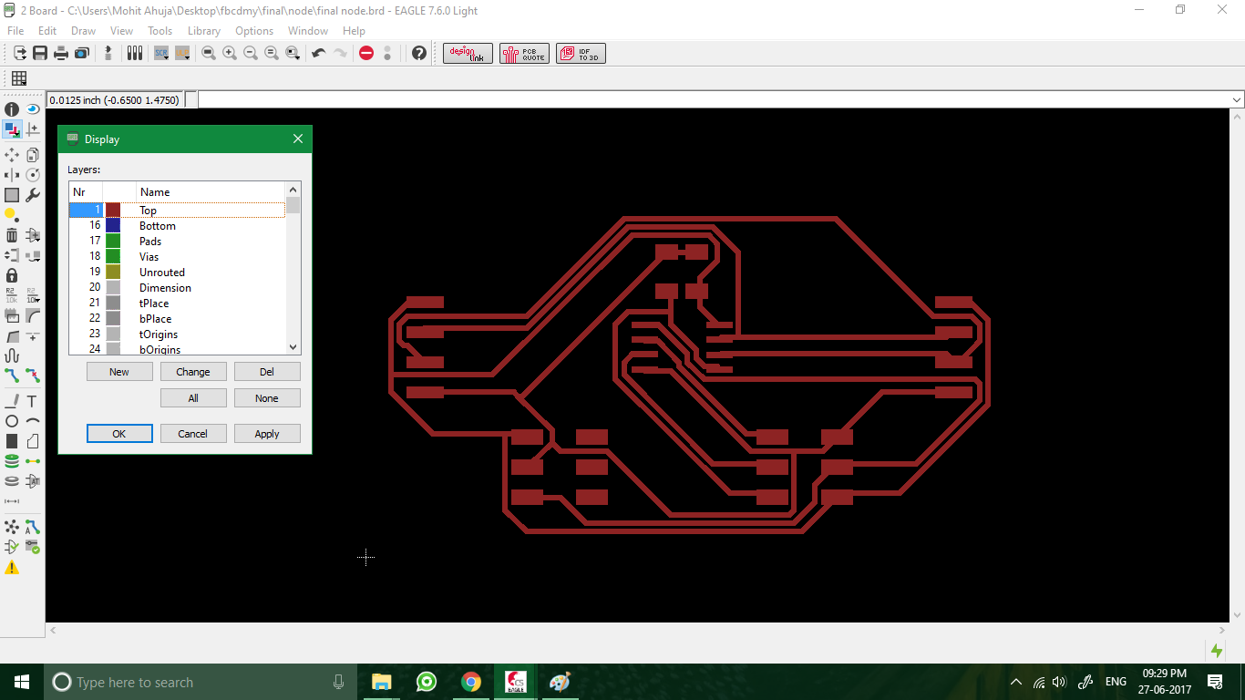
Step 10: Layer settings
I then started making the PCB Fab Files Layer by layer.
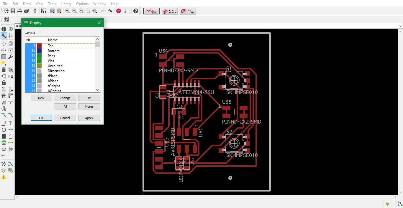
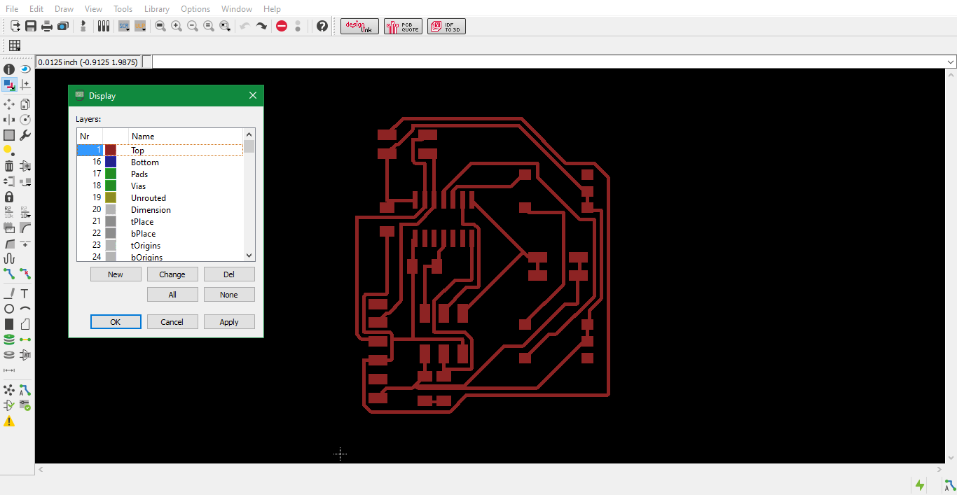
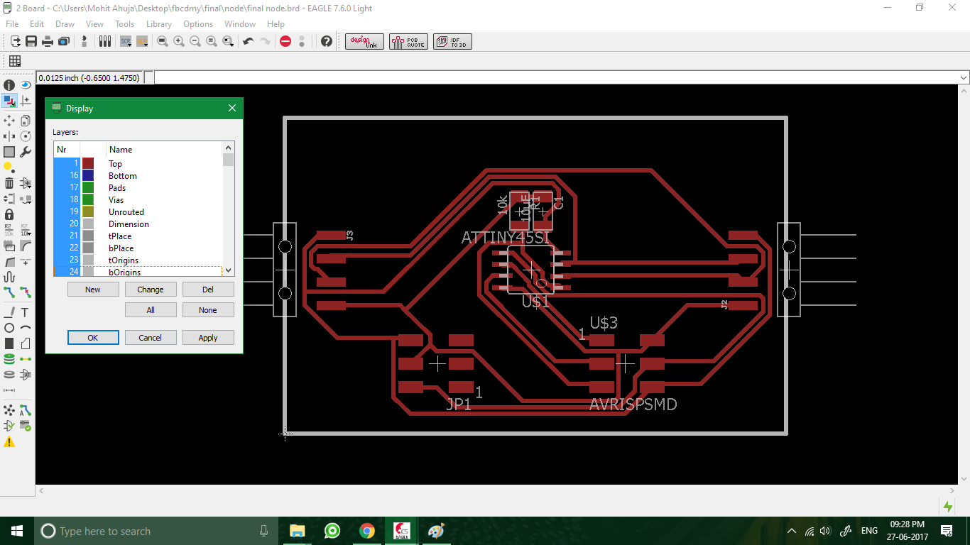
Step 11: Showing details layers
First all the relevant layers were selected for exporting.
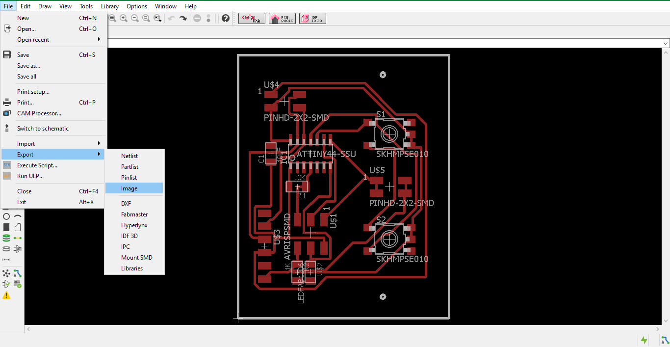
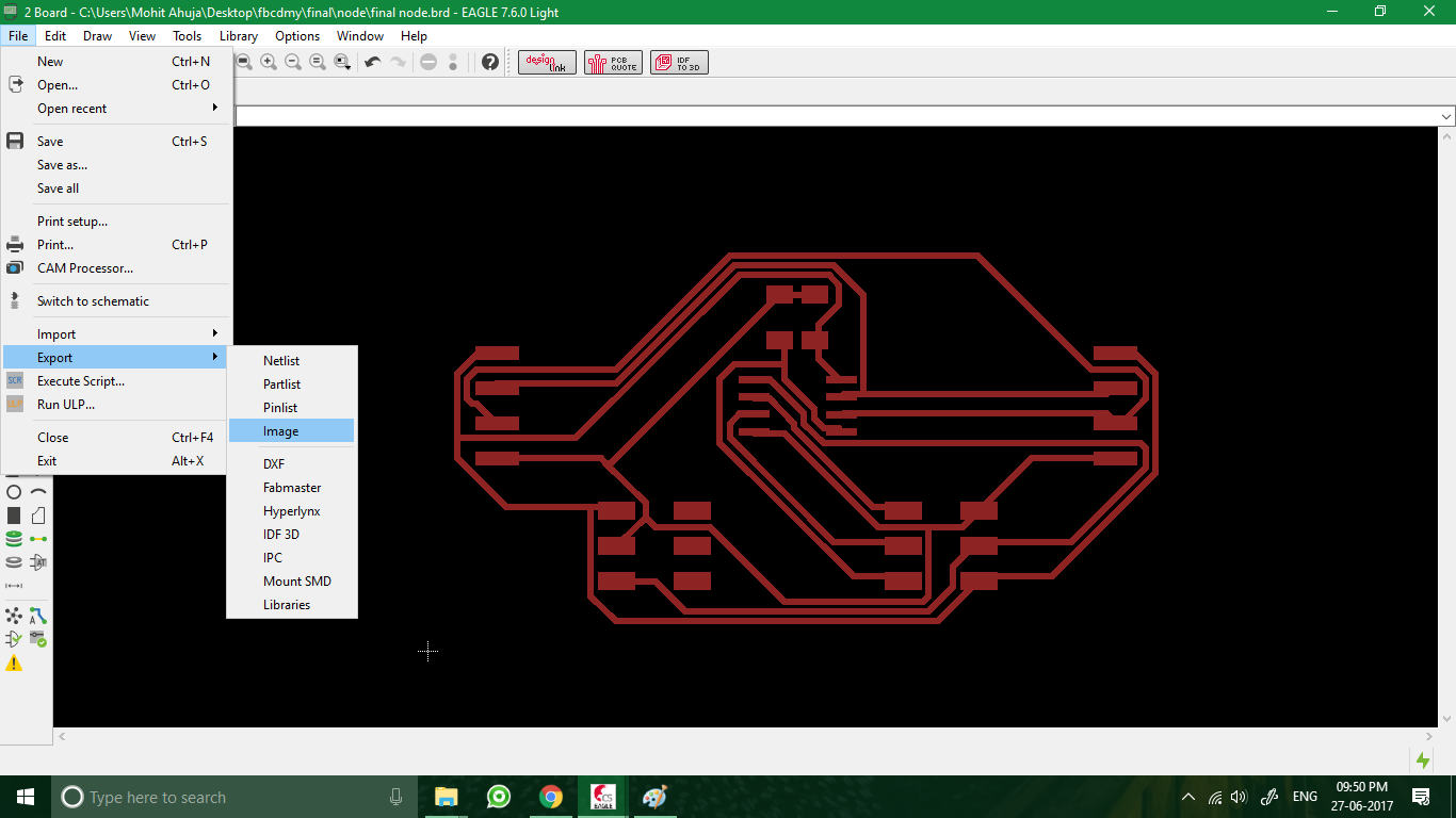
Step 12: Export as image
For exporting the image I navigated to File > Export > Image.
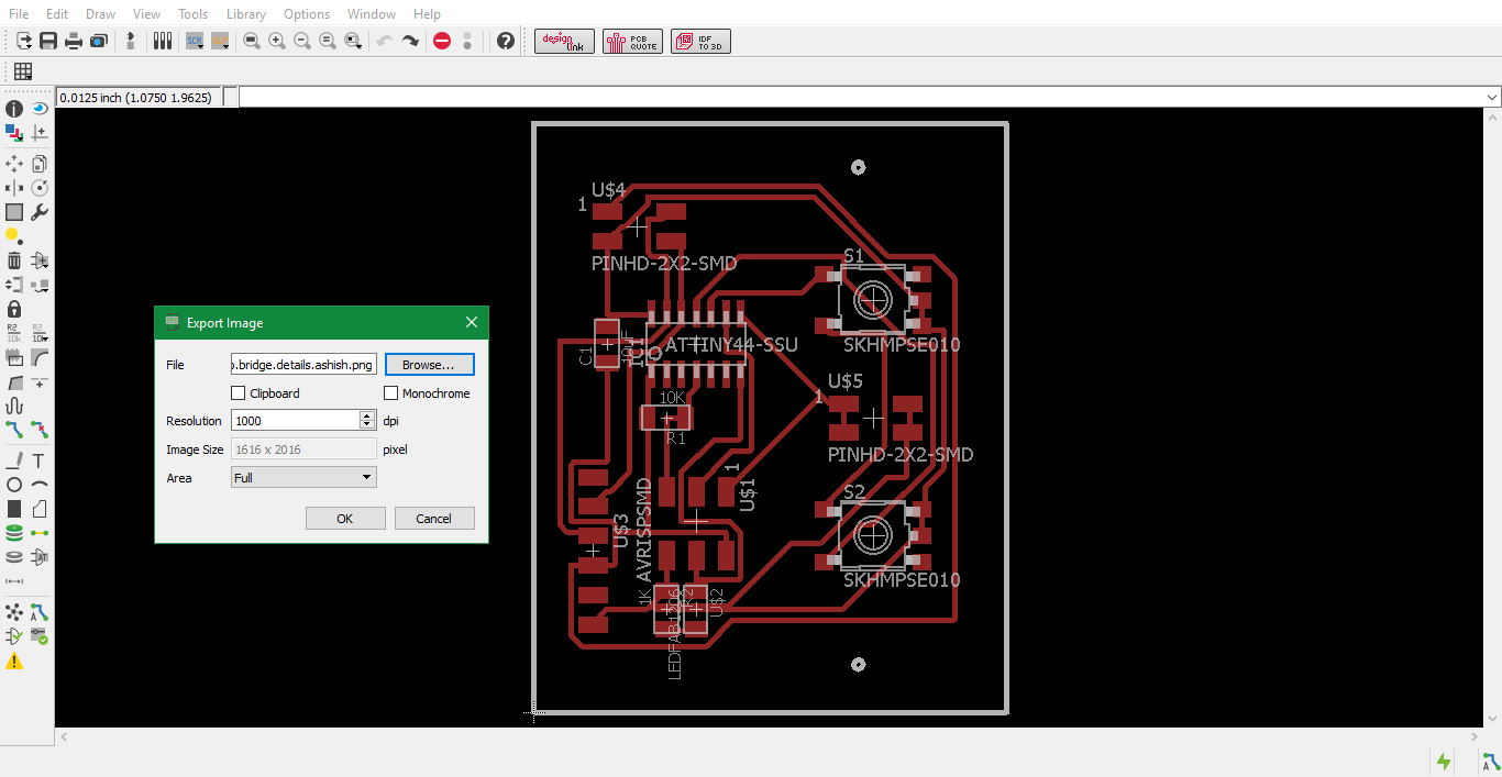
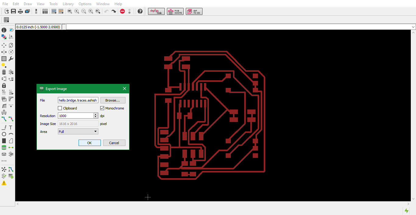
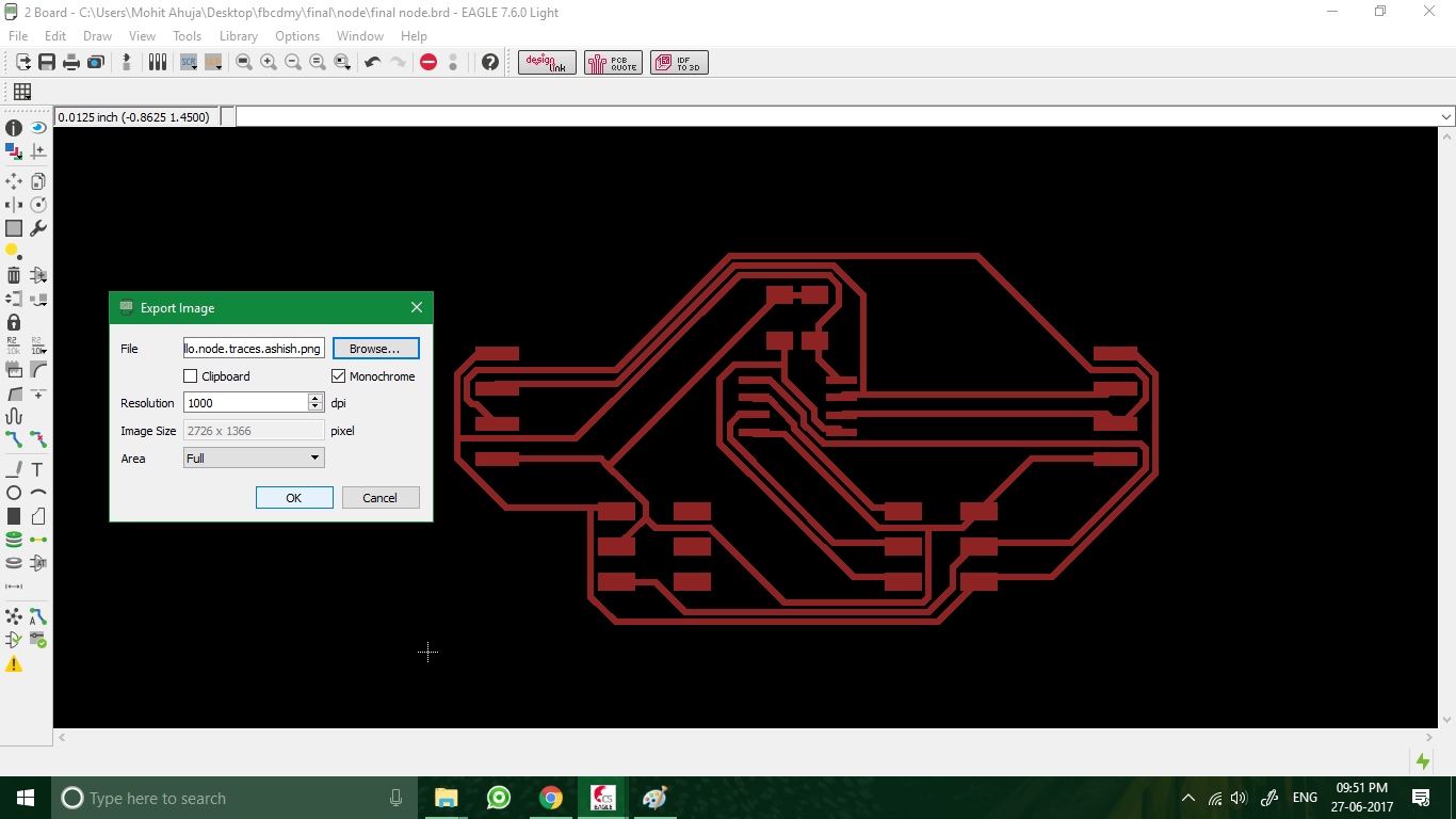
Step 13: Export window details
I exported the file with a resolution of 1000.
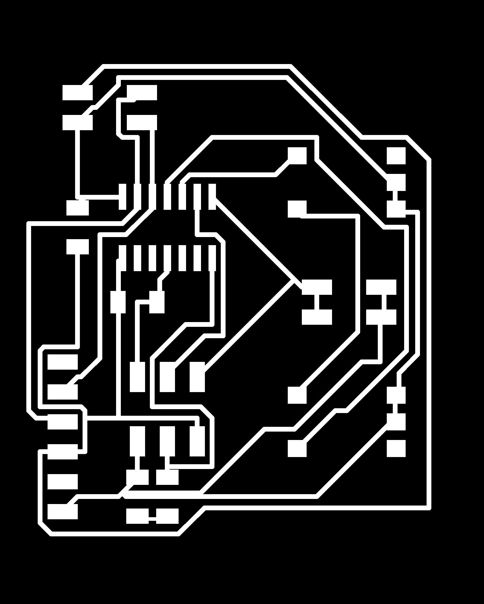
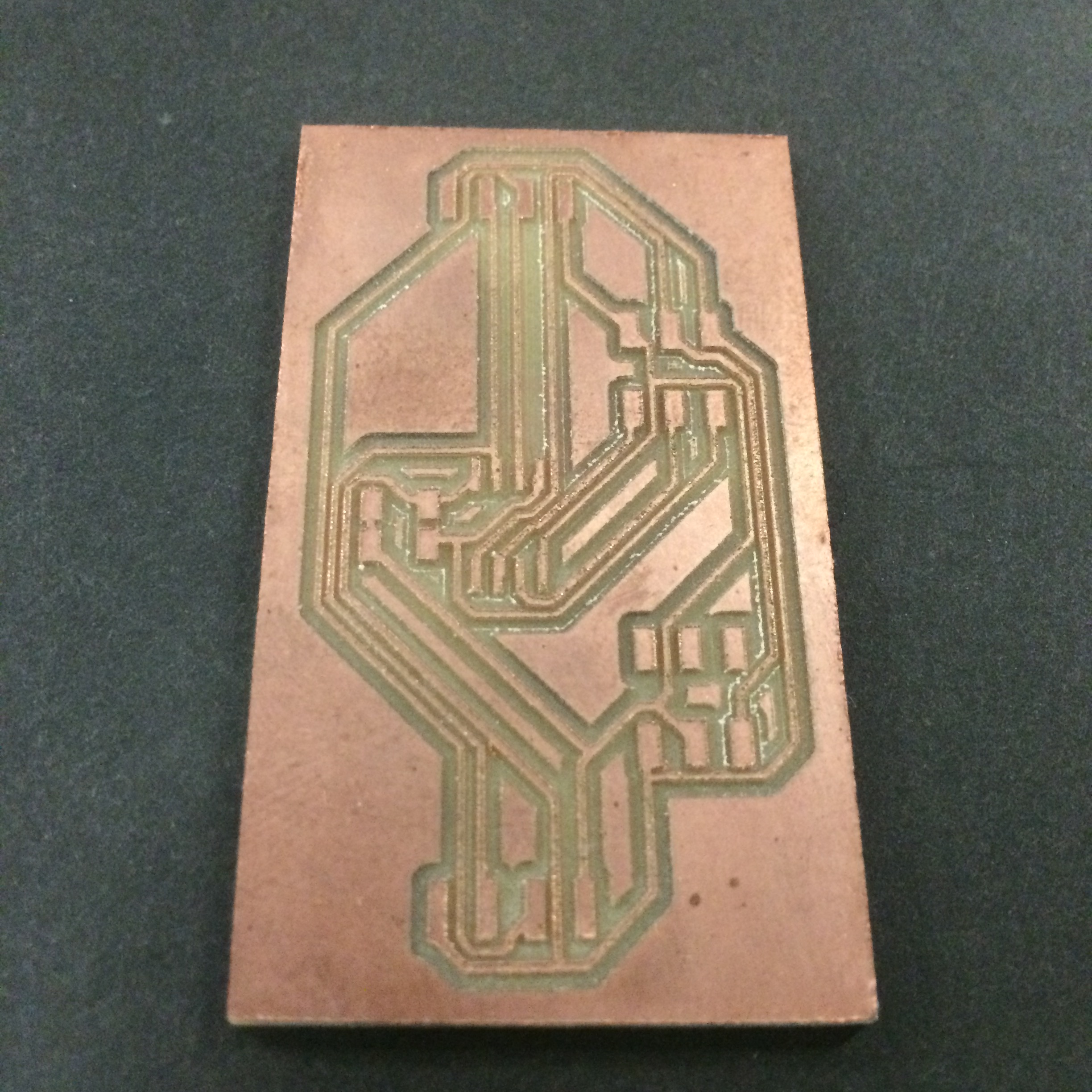
Step 14: Showing traces layer
Next I selected the Top layer to select the traces.
Step 15: Export window traces
I exported this file with monochrome setting and a resolution of 1000.
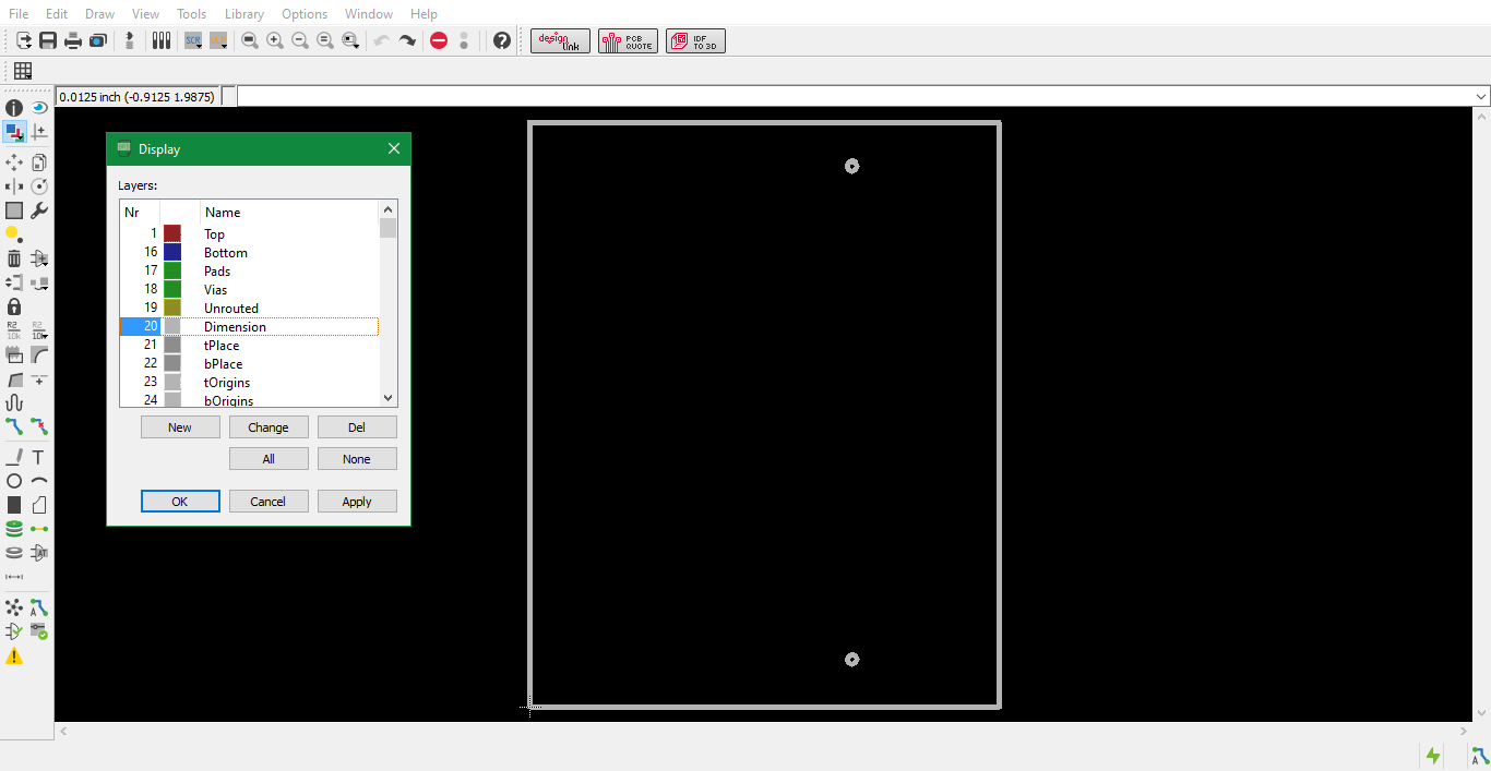
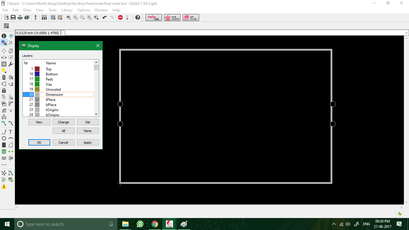
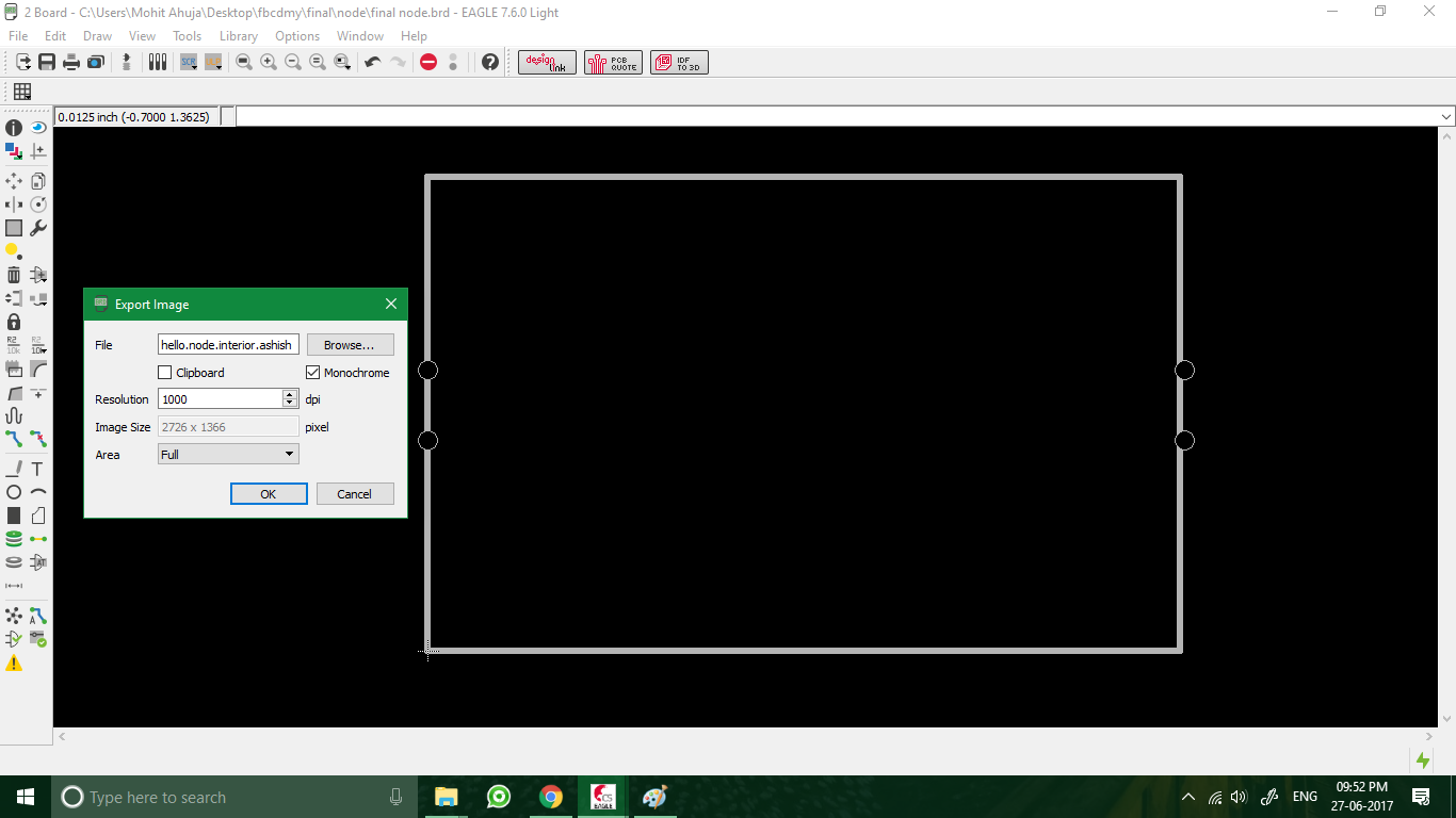
Step 16: Showing interior layer
Lastly I selected the Dimension layer to select the interior.
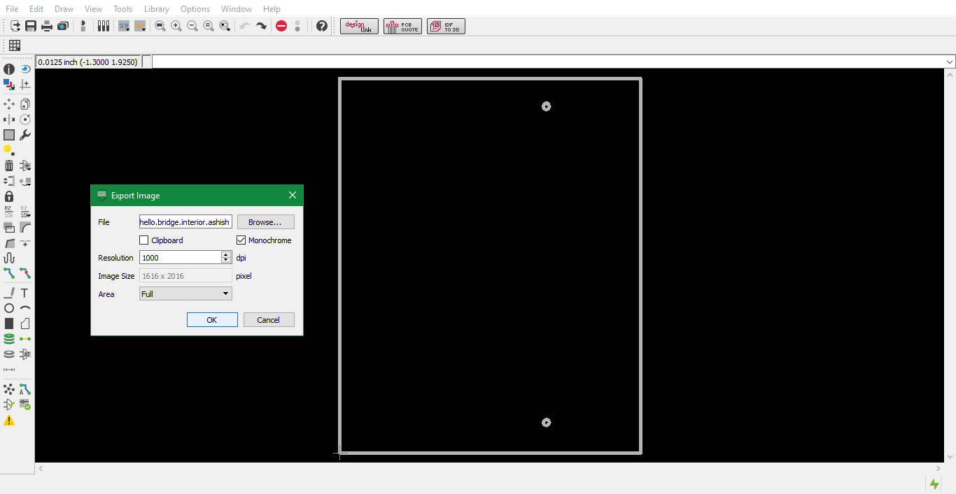
Step 17: Export window interior
I exported this file with monochrome setting and a resolution of 1000.
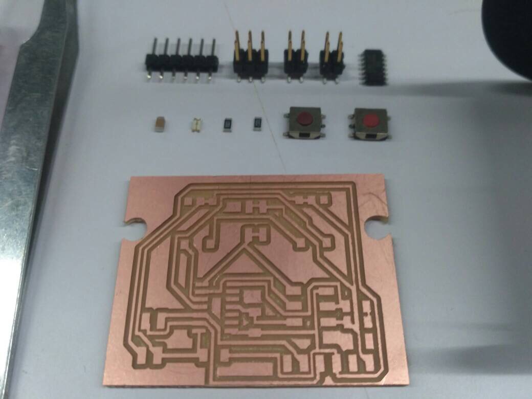
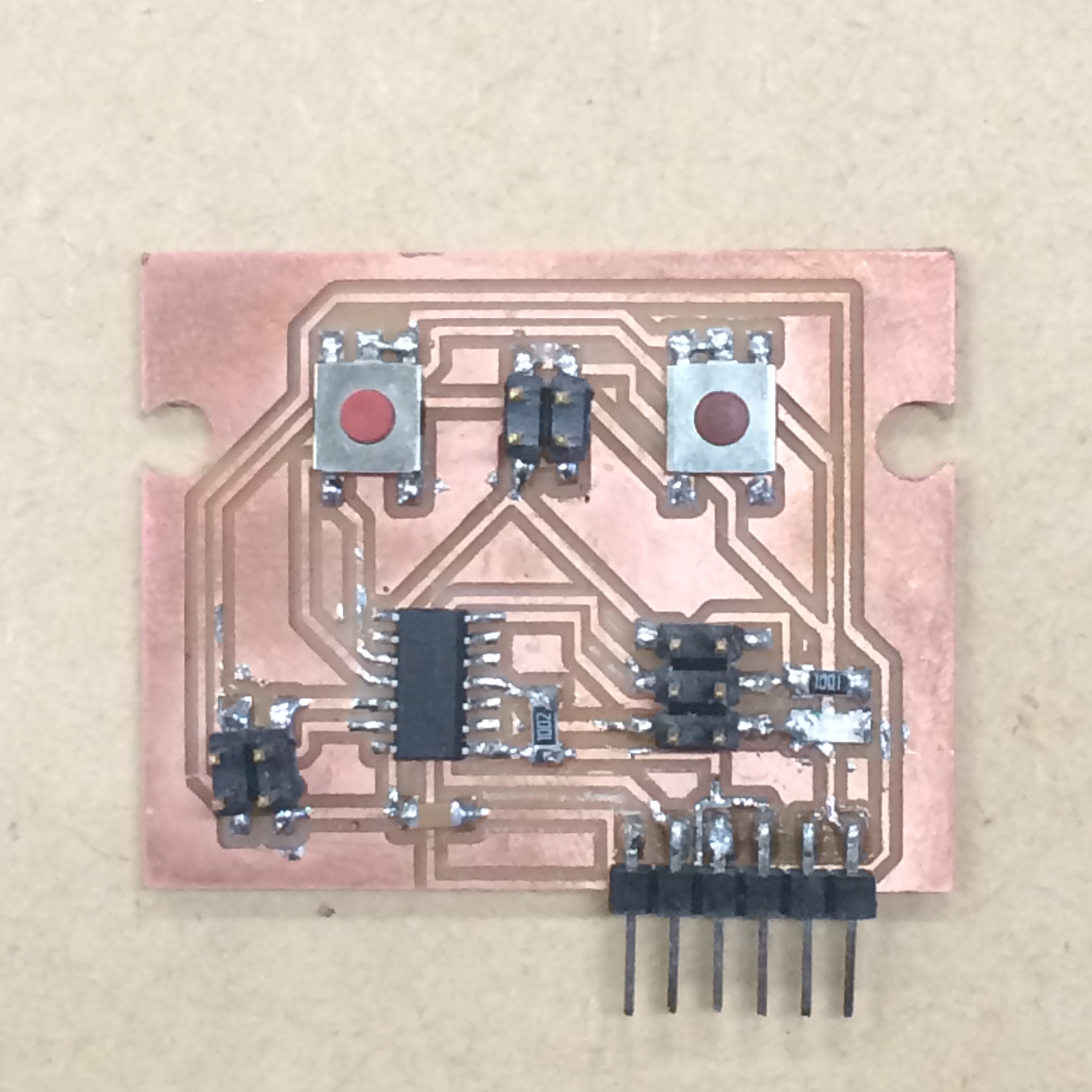
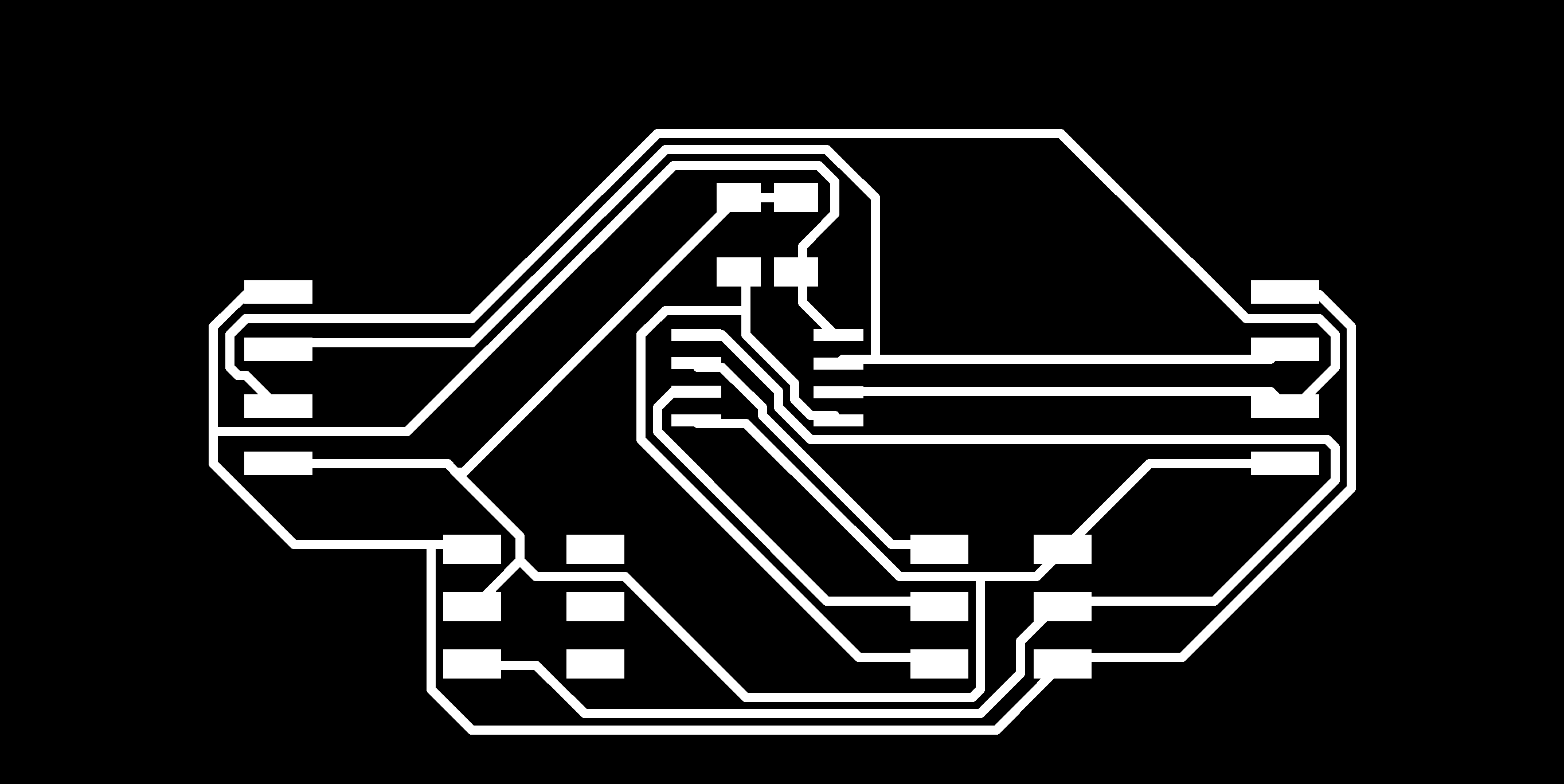
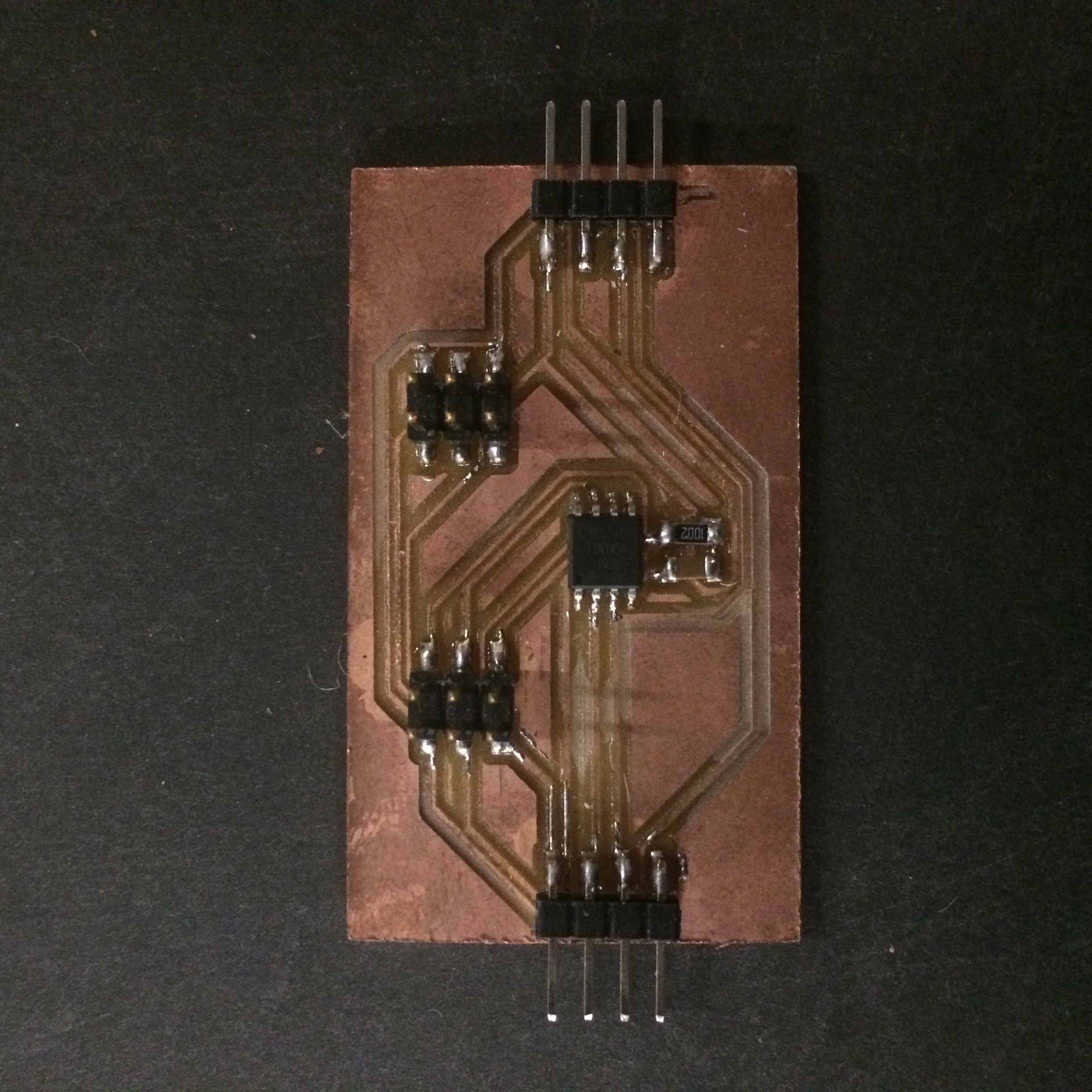
Final Circuit Board- Bridge
Designing the NOde board
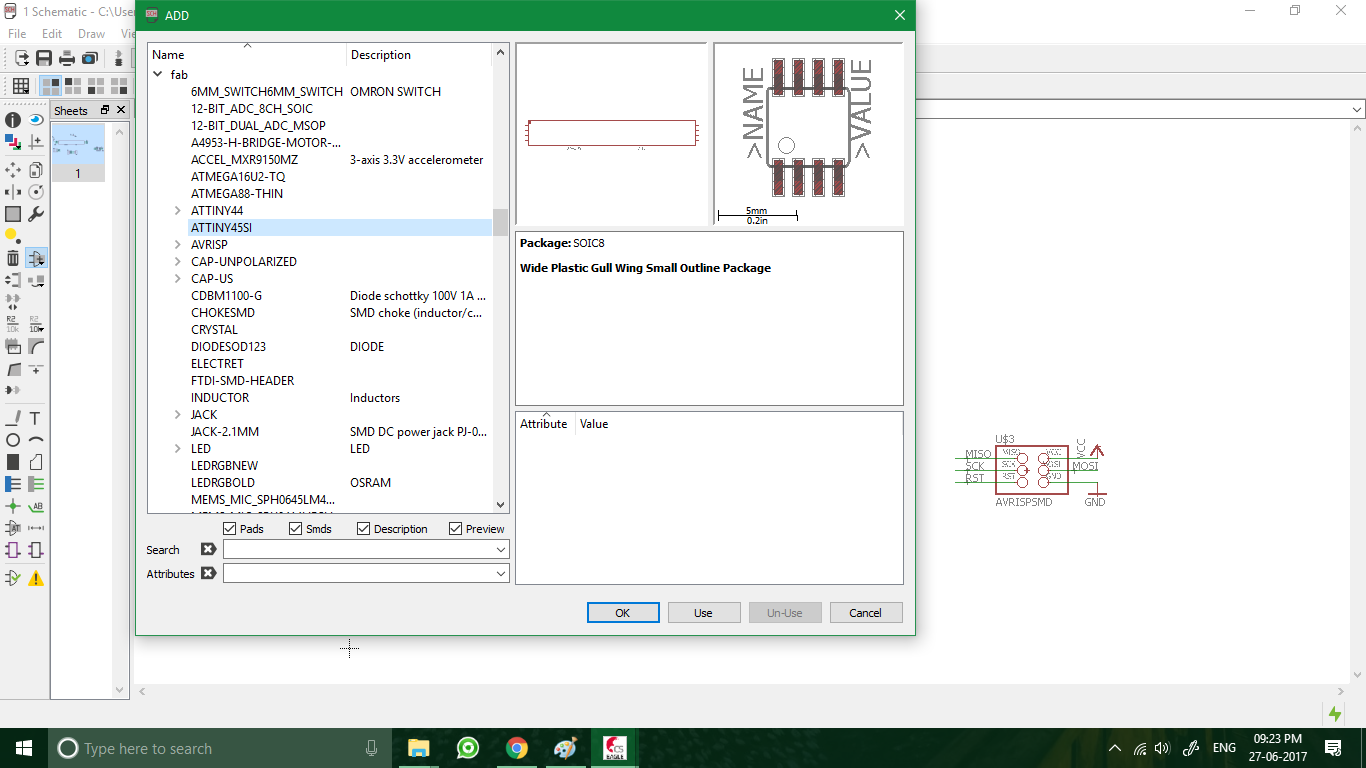
Step 1: Adding components to schematic
I began with adding components to the schematic window. The node has an ATtiny45 as opposed to the ATtiny44 chip on the bridge. The number of components on the node is also considerably much lesser.
Step 2: Schematic
After adding all the components and making the relevant connections, the schematic was complete.

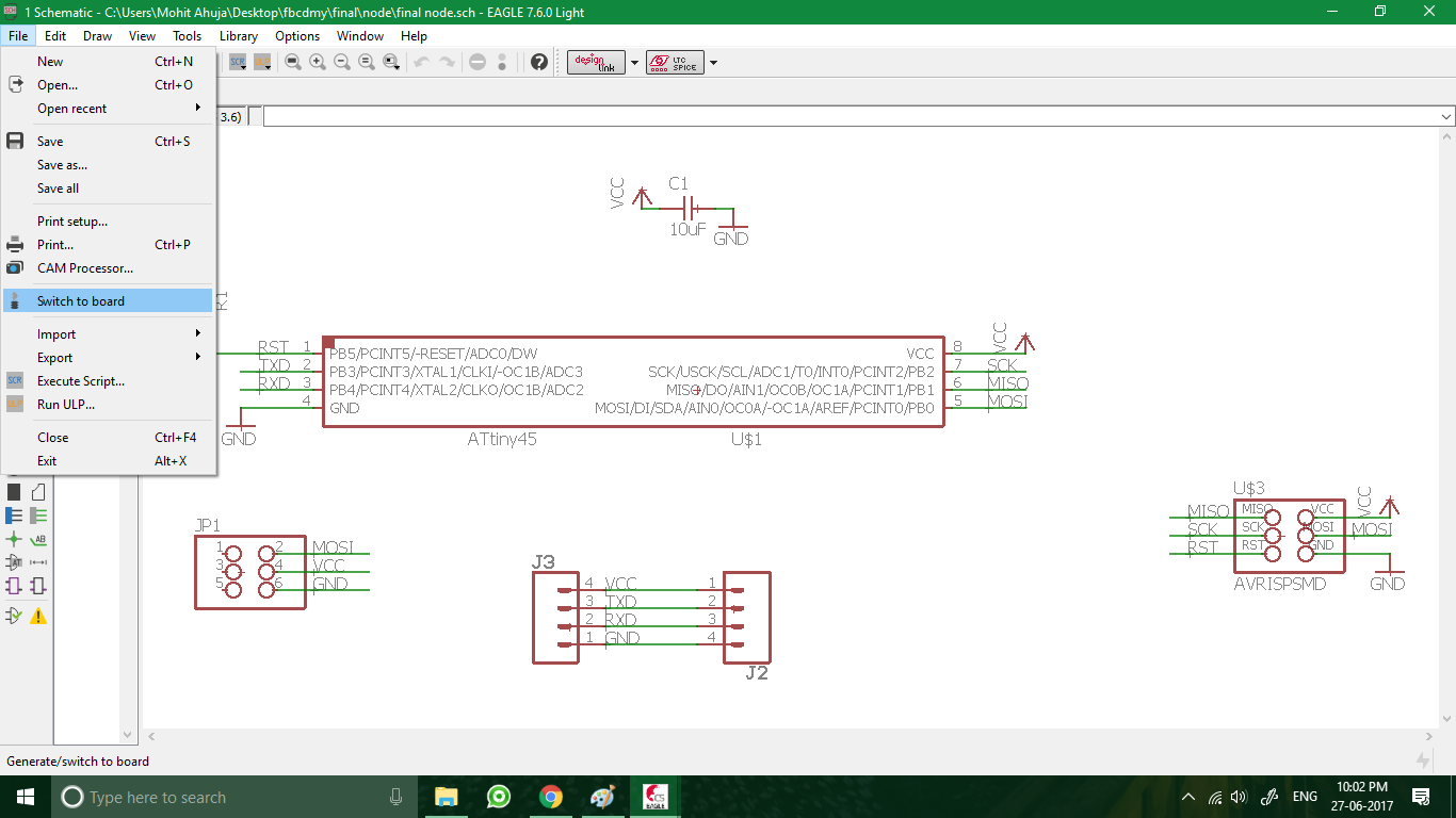
Step 3: Switch to board
Once the schematic was complete, I navigated to File > Switch to board.
Step 4: Board created
The Board Layout window was created, where all the components with their connections in ratsnest form are given.
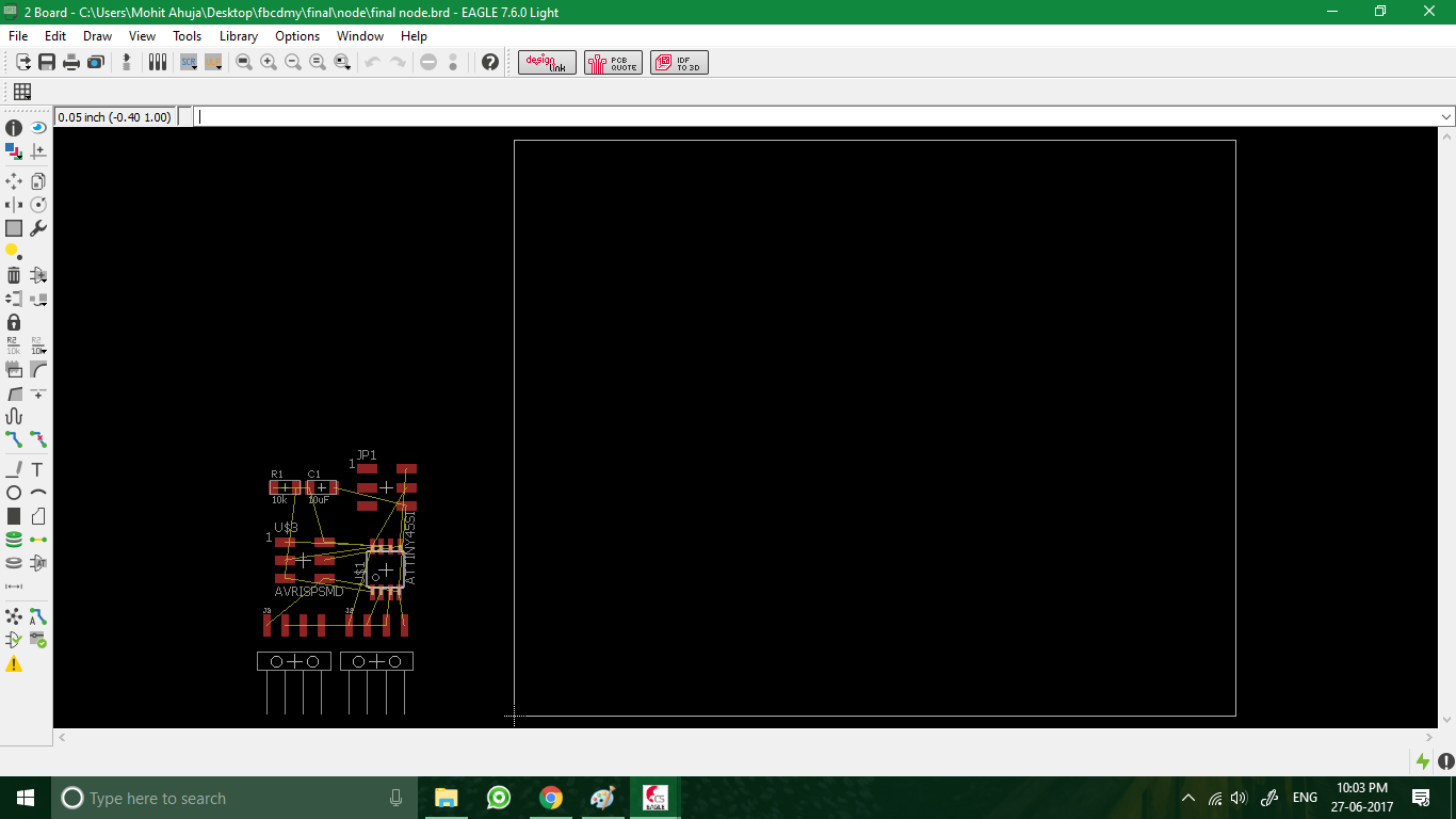
Step 5: Before autorouting
I rearranged the components according to my requirements and resized the PCB. I also made the interior of the board.
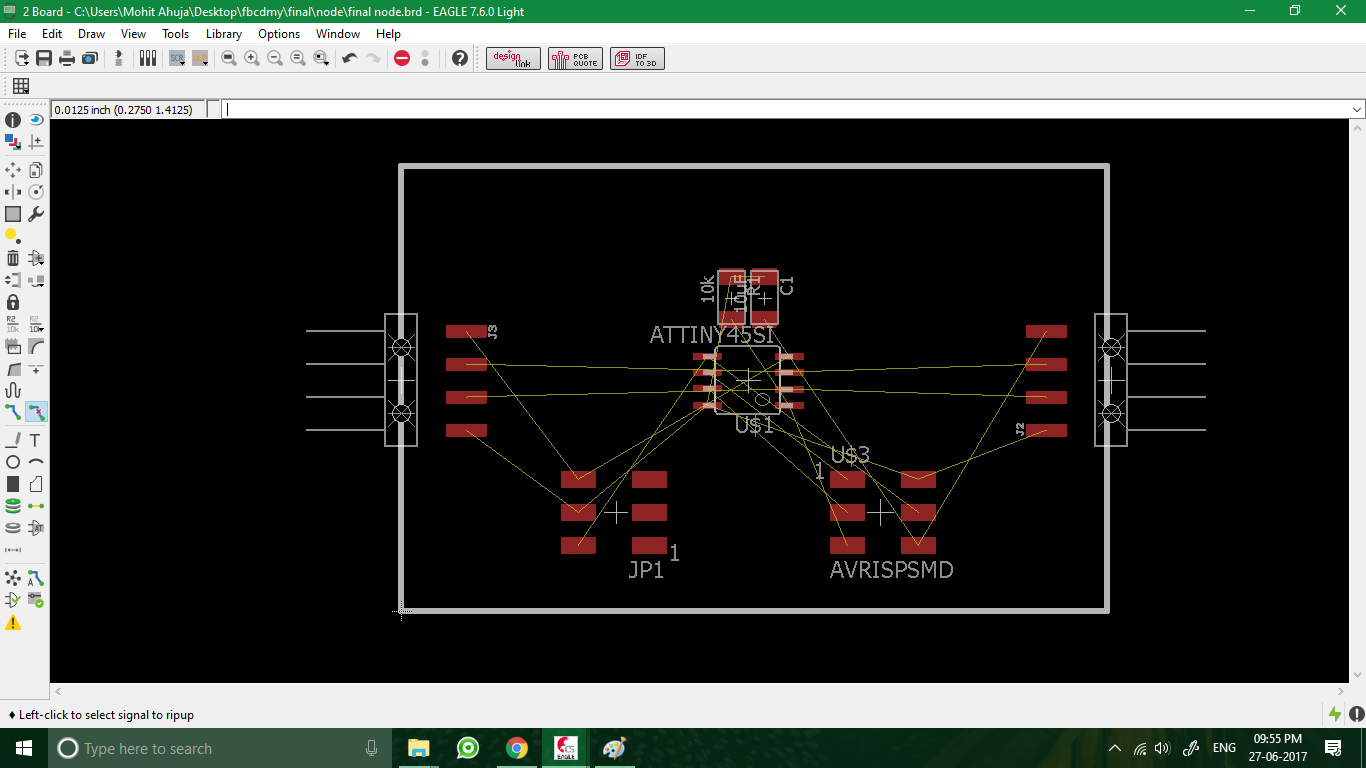
Step 6: net classes
After that I edited the net classes to with the following settings:
Step 7: Autorouting begins
Once the net classes are chosen, I began autorouting with the following settings:
Step 8: Autorouting window
Autorouting window showing the running threads for different designs.
Step 9: Autoroute complete
The best possible design was chosen for the PCB and the circuit design was checked with DRC to reveal no errors.
Step 10: Export as image
For exporting the image I navigated to File > Export > Image.
Step 11: Showing traces layer
I selected the Top layer to select the traces. I then started making the PCB Fab Files Layer by layer.
Step 12: Saving traces
I exported this file with monochrome setting and a resolution of 1000.
Step 13: Showing interior layer
Next I selected the Dimension layer to select the interior.
Step 14: Saving interior
I exported this file with monochrome setting and a resolution of 1000.
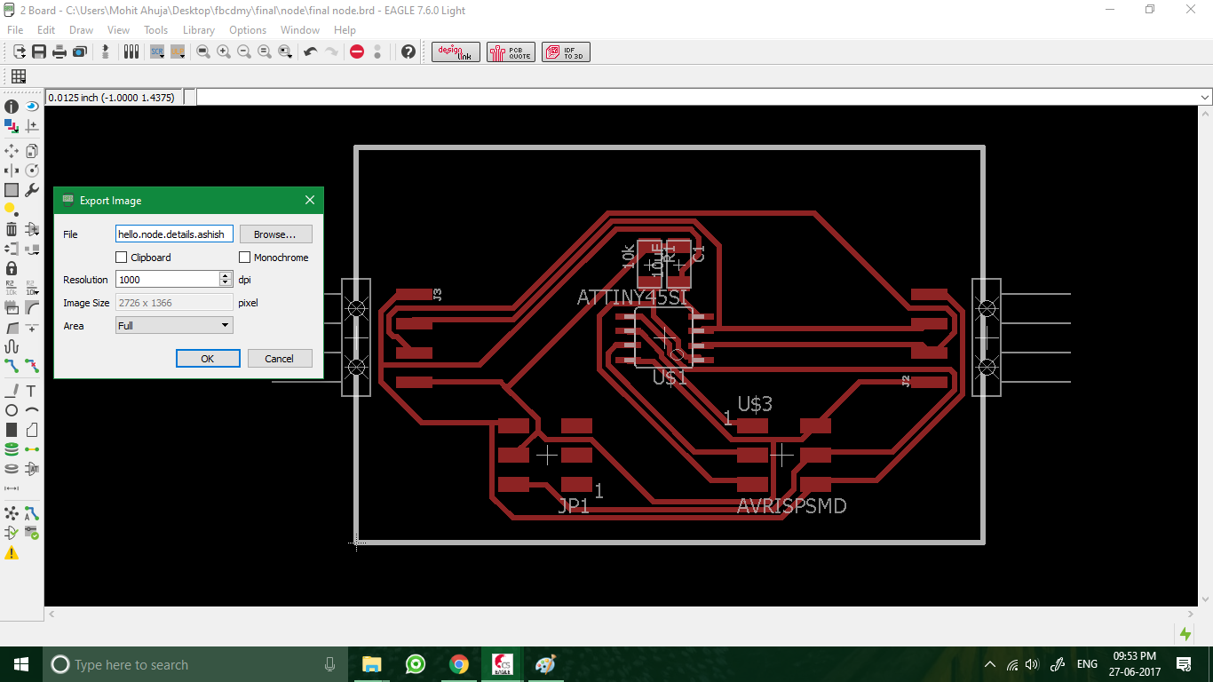
Step 15: Showing details layers
Lastly all the relevant layers were selected for exporting.
Step 16: Saving details
I exported the file with a resolution of 1000.
Step 17
Done
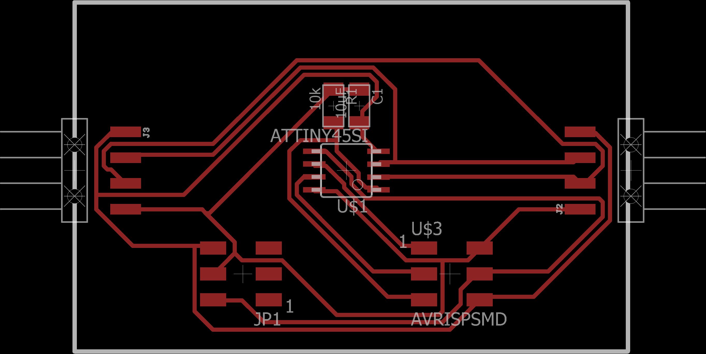
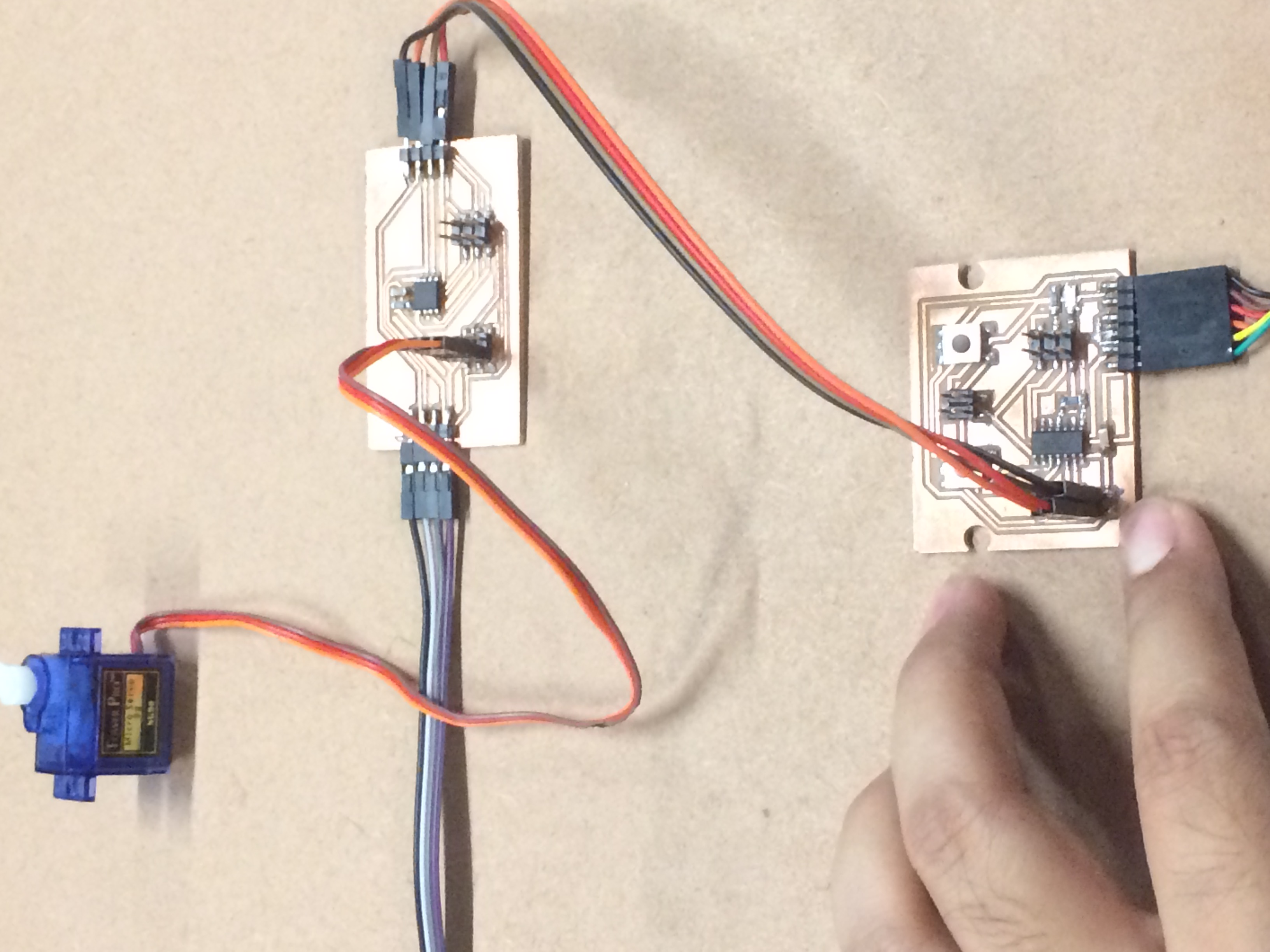
Final Circuit Board- Node
Programming
Bridge
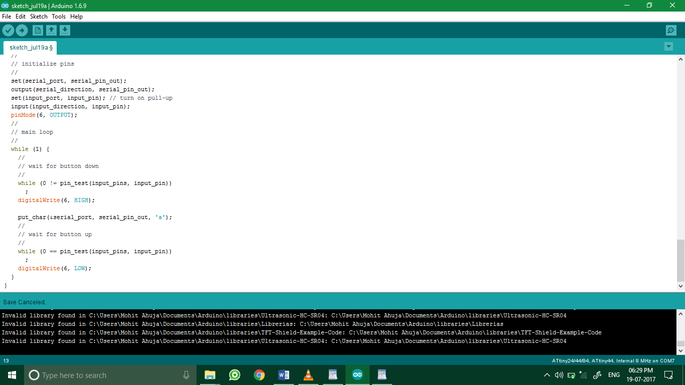
Step 1: The Bridge has two pushbuttons to toggle between different modes. But to demonstrate the functionality we need to use only one. I have used Neil’s code for the hello.button board. I added some modifications with the help of Mohit Ahuja. The button that I intend to use is attached to pin PA2. Pressing the button sends a character “a” on the serial port. The corresponding nodes will respond to the serial command given by the bridge.
Step 2: I selected the settings for uploading the code to the bridge. They are:
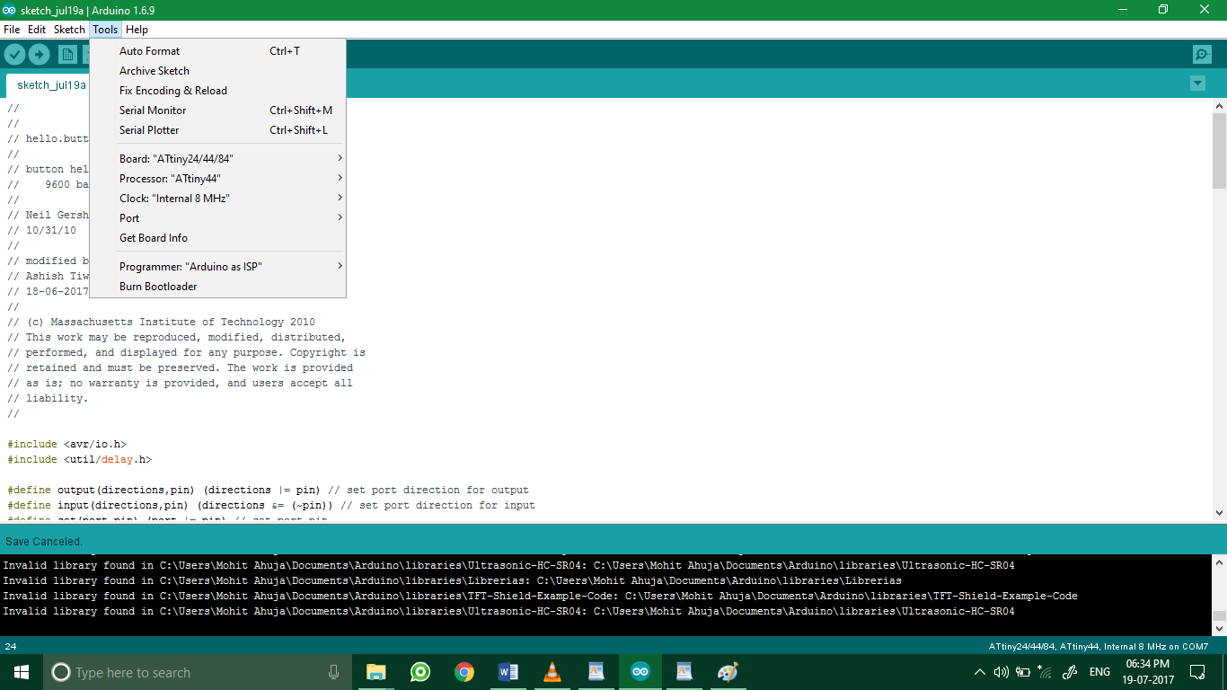
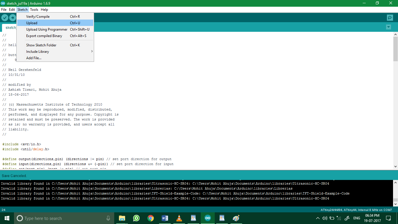
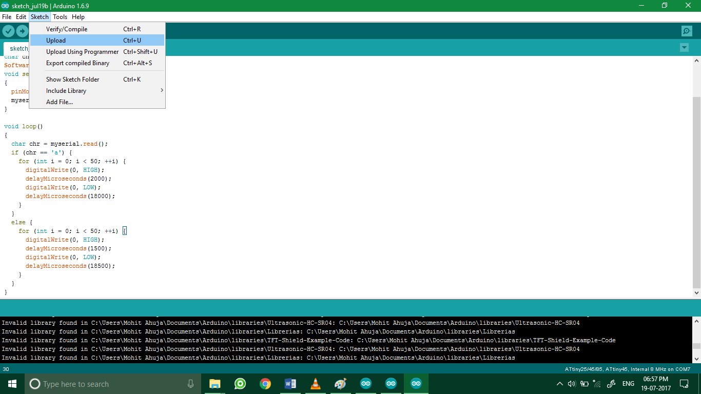
Step 3: After burning the bootloader, I uploaded the code by clicking on Sketch > Upload. Next I proceeded onto coding the node.
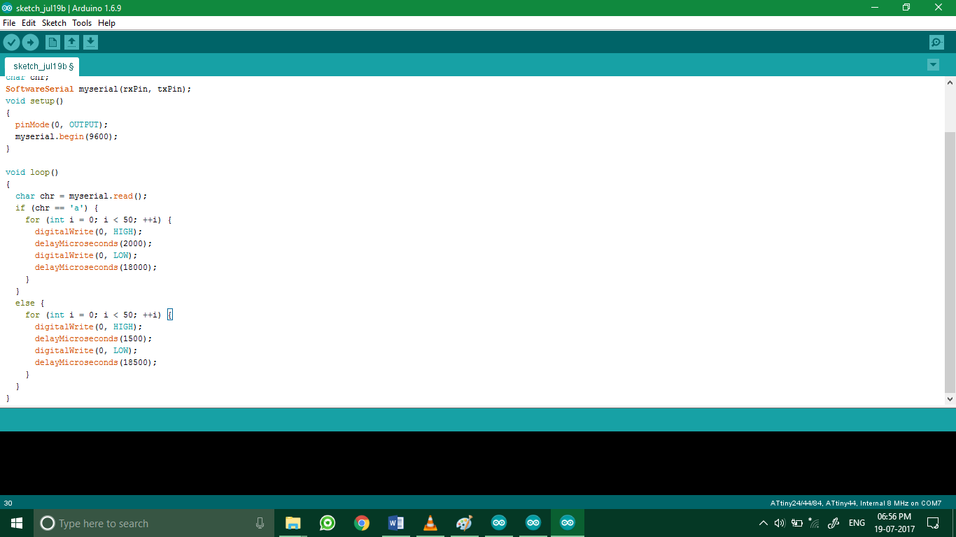
Step 1: The node is programmed in such a way that it has an address and different nodes can have different addresses if need be. The program looks for the address character on its serial port and if it gets the address, then it rotates the servo 45 degrees for almost a second, and then returns it to its original place. One only needs to change values in the if statement to change the desired address. The variable “chr” takes care of checking what is being sent on the serial port.
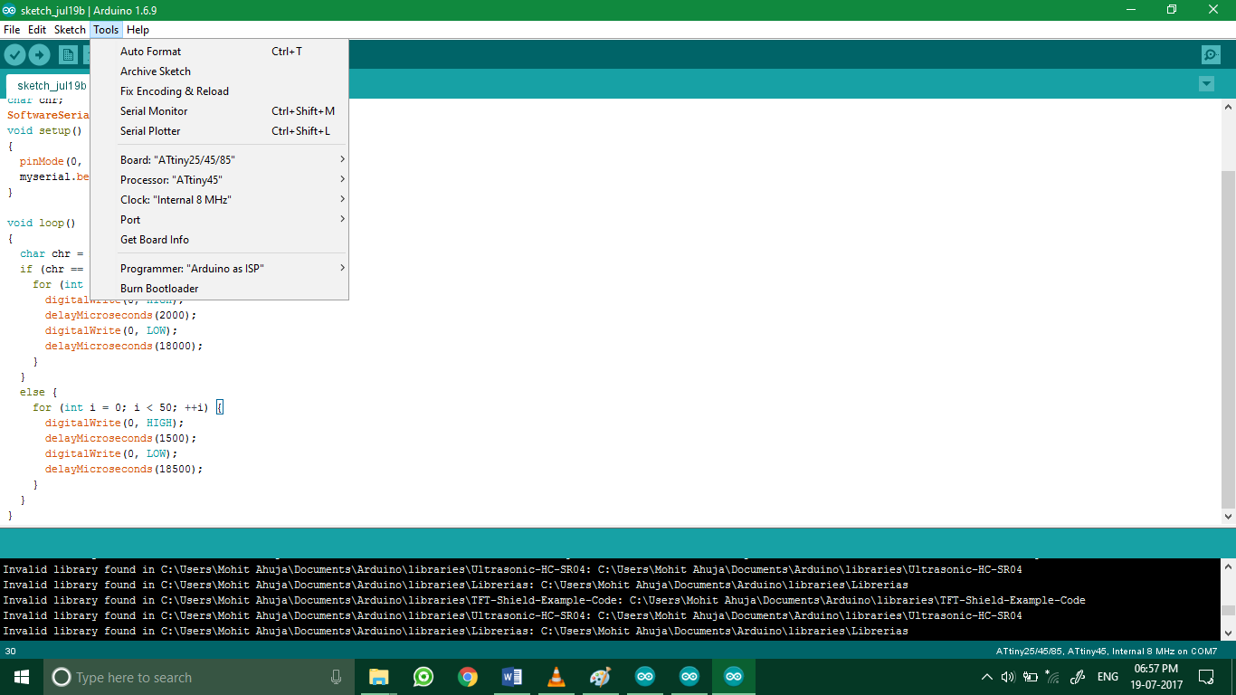
Step 2: The settings vary slightly for the node from the bridge. These settings are:
Step 3: After the bootloader was burnt, I proceeded to upload the code using Sketch > Upload.
After all the codes were uploaded, I connected all the boards together and tested them. The video shows a demonstration of the working network. A point to take care was that the bridge’s Tx pin was connected to the node’s Rx pin and vice-versa.
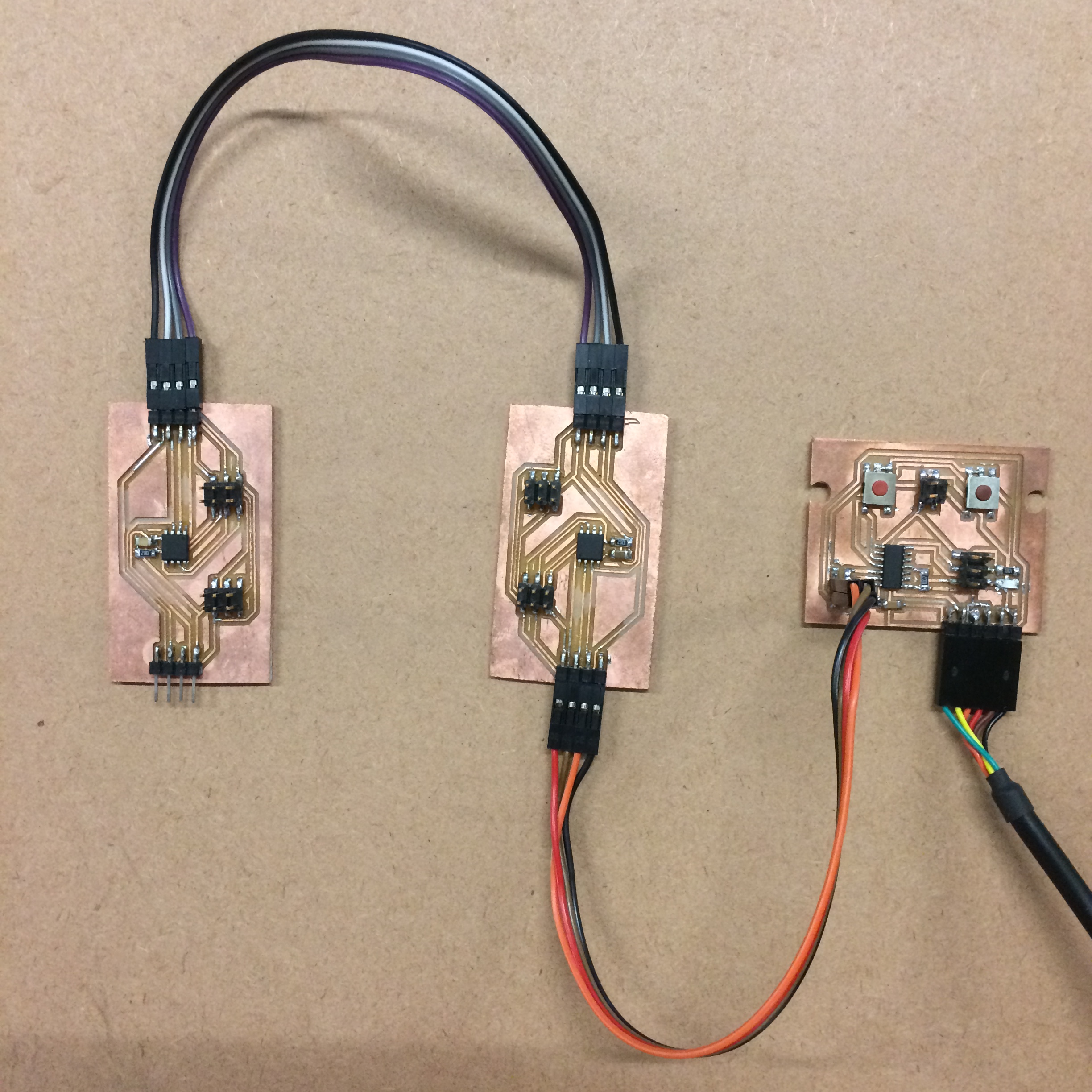
Communication between Bridge and Node
HOST COMPUTER >> BRIDGE BOARD >> NODE BOARD >> SERVO
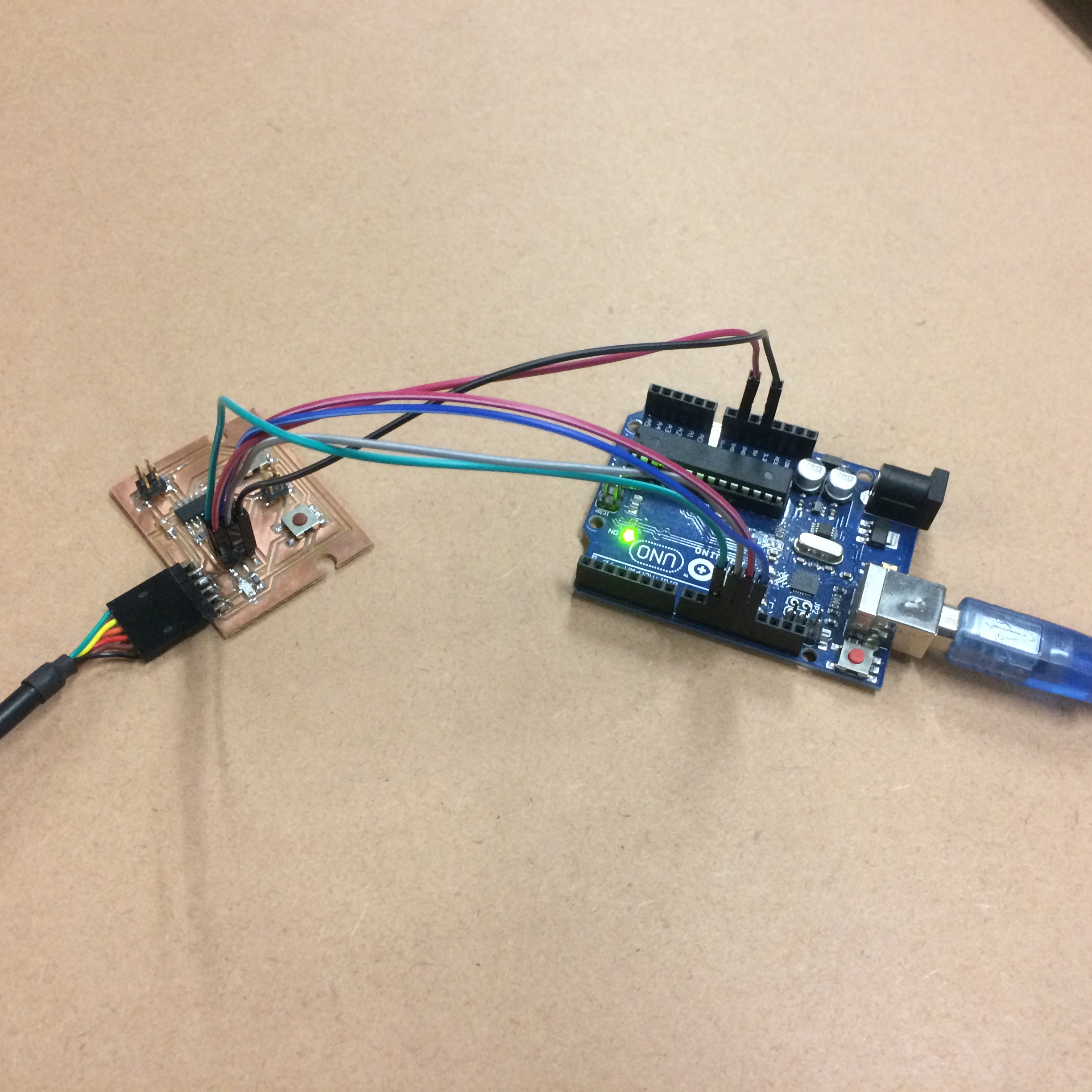
Using the Arduino UNO to program the board
A bridge board and two node boards, in the final project using the same system I use 5 node boards
Demo video
Code
Bridge board code
    //
//
// hello.button.45.c
//
// button hello-world
//    9600 baud FTDI interface
//
// Neil Gershenfeld
// 10/31/10
//
// modified by
// Ashish Tiwari, Mohit Ahuja
//
// (c) Massachusetts Institute of Technology 2010
// This work may be reproduced, modified, distributed,
// performed, and displayed for any purpose. Copyright is
// retained and must be preserved. The work is provided
// as is; no warranty is provided, and users accept all
// liability.
//

#include <avr/io.h>
#include <util/delay.h>

#define output(directions,pin) (directions |= pin) // set port direction for output
#define input(directions,pin) (directions &= (~pin)) // set port direction for input
#define set(port,pin) (port |= pin) // set port pin
#define clear(port,pin) (port &= (~pin)) // clear port pin
#define pin_test(pins,pin) (pins & pin) // test for port pin
#define bit_test(byte,bit) (byte & (1 << bit)) // test for bit set
#define bit_delay_time 102 // bit delay for 9600 with overhead
#define bit_delay() _delay_us(bit_delay_time) // RS232 bit delay
#define half_bit_delay() _delay_us(bit_delay_time/2) // RS232 half bit delay

#define input_port PORTA
#define input_direction DDRA
#define input_pin (1 << PA2)
#define input_pins PINA
#define serial_port PORTA
#define serial_direction DDRA
#define serial_pin_out (1 << PA1)

void put_char(volatile unsigned char *port, unsigned char pin, char txchar) {
  //
  // send character in txchar on port pin
  //    assumes line driver (inverts bits)
  //
  // start bit
  //
  clear(*port, pin);
  bit_delay();
  //
  // unrolled loop to write data bits
  //
  if bit_test(txchar, 0)
    set(*port, pin);
  else
    clear(*port, pin);
  bit_delay();
  if bit_test(txchar, 1)
    set(*port, pin);
  else
    clear(*port, pin);
  bit_delay();
  if bit_test(txchar, 2)
    set(*port, pin);
  else
    clear(*port, pin);
  bit_delay();
  if bit_test(txchar, 3)
    set(*port, pin);
  else
    clear(*port, pin);
  bit_delay();
  if bit_test(txchar, 4)
    set(*port, pin);
  else
    clear(*port, pin);
  bit_delay();
  if bit_test(txchar, 5)
    set(*port, pin);
  else
    clear(*port, pin);
  bit_delay();
  if bit_test(txchar, 6)
    set(*port, pin);
  else
    clear(*port, pin);
  bit_delay();
  if bit_test(txchar, 7)
    set(*port, pin);
  else
    clear(*port, pin);
  bit_delay();
  //
  // stop bit
  //
  set(*port, pin);
  bit_delay();
  //
  // char delay
  //
  bit_delay();
}

int main(void) {
  //
  // main
  //
  // set clock divider to /1
  //
  CLKPR = (1 << CLKPCE);
  CLKPR = (0 << CLKPS3) | (0 << CLKPS2) | (0 << CLKPS1) | (0 << CLKPS0);
  //
  // initialize pins
  //
  set(serial_port, serial_pin_out);
  output(serial_direction, serial_pin_out);
  set(input_port, input_pin); // turn on pull-up
  input(input_direction, input_pin);
  pinMode(6, OUTPUT);
  //
  // main loop
  //
  while (1) {
    //
    // wait for button down
    //
    while (0 != pin_test(input_pins, input_pin))
      ;
    digitalWrite(6, HIGH);

    put_char(&serial_port, serial_pin_out, 'a');
    //
    // wait for button up
    //
    while (0 == pin_test(input_pins, input_pin))
      ;
    digitalWrite(6, LOW);
  }
}
Node board code
      #include<SoftwareSerial.h>

int rxPin = 3;
int txPin = 4;
char chr;
SoftwareSerial myserial(rxPin, txPin);
void setup()
{
  pinMode(0, OUTPUT);
  myserial.begin(9600);
}

void loop()
{
  char chr = myserial.read();
  if (chr == 'a') {
    for (int i = 0; i < 50; ++i) {
      digitalWrite(0, HIGH);
      delayMicroseconds(2000);
      digitalWrite(0, LOW);
      delayMicroseconds(18000);
    }
  }
  else {
    for (int i = 0; i < 50; ++i) {
      digitalWrite(0, HIGH);
      delayMicroseconds(1500);
      digitalWrite(0, LOW);
      delayMicroseconds(18500);
    }
  }
}
Links
Code for bridge in .inoEagle board layout for Bridge
Eagle schematic for Bridge
Eagle board layout for Node
Eagle schematic for Node
Code for Node-board in .ino