This week is all about taking the simple Echo Hello World board from fablab archives, redesign it and add some new functionalities.
The objectives of this assignment are:
- Redraw the echo hello-world board.
- Add (at least) a button and LED (with current-limiting resistor).
- Check the design rules, make it, and test it.
- Extra credit: simulate its operation.
- Extra credit: measure its operation.
Redraw the Echo Hello-World Board
There are several softwares available for PCB design Prof. Niel in his lecture provided an exhaustive list of software ranging from free open source project to high end industrial grade one.

|

|

|

|
|
►Free,Open Source ►Modest Functionality. |
►Relatively low cost ►Suitable for intermediate users ►Widely supported and documented. |
►High liecense cost. ►Suitable for advanced user ►Allows many other funcationalities. |
►High liecense cost. ►Capable of IC design. |
The start of any Printed circuit board design starts from selection of components (based on circuit requirements). The interconnect of these components is commonly known as electrical schematic . Every electrical component is typically represented by a symbol and this makes it possible to understand the behaviour of the system. Altough it may not be completely clear in the presence of non-linear devices like ICs.
Select Component Library
To work with the all the discrete and analog components which are already available in the inventory of the Fablab. I downloaded the eagle parts library from here . This library contains information about the electrical characteristics (number of pins, electrical rating) as well as the physical characteristics such as package type, dimensions and number of components per IC.
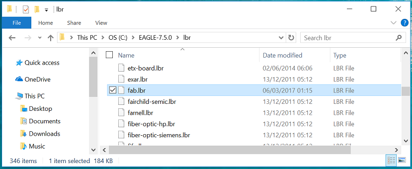
Library is copied in location /eagle/lbr/
Electrical schematic design is simply the scheme of electrical connections between the different discrete and integrated circuit components. Each component is represented by a symbol which is typically located in eagle library files. The figure below illustrates an electrical schematic with some discrete components connected to a micro-controller.

The design of PCB is an elaborate process which requires complete understanding of electrical as well as physical characteristics of integrated circuits. All commercial integrated circuits are identified through unique name. The desired components can be identified through internet search, through some well known websites like Octapart or distributor portals like Farnell , digikey and mouser etc. All manufacturers provide technical details and application notes in the data sheets.
The graphical illustration explaining the design process is as follows:
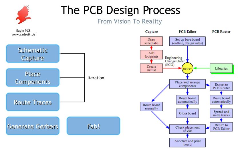
Source: Cadsoft.com
An excellent video illustrating the complete design process using eagle is as follows:
Electrical Schematic Design
As per requirement we had to redraw the echo hello world board. The PCB layout of this board in available here .
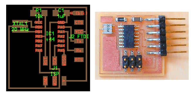
Source
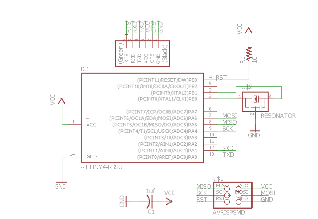
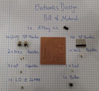
Carefully looking at the PCB board layout, I identified the following components are present in this circuit.
- AtTiny44a in SOIC package.
- 1 2x3 Pin right angle male header.
- 1 1x6 Pin SMD type male headers.
- 20 MHz local oscillator.
- 1uf capacitor.
- 10k Ohm resistor.
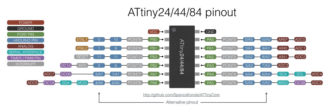
Now refering to the pin diagram and the data sheet of AT tiny44 we can notice many pin connections. A few important connections are as follows:
- Pin 1 and 14 need to be connected with Vcc and Gnd respectively.
- Pin 2 and 3 (also called PB0 and PB1) need to connected to XTAL.
- Pin 4 needs to be connected with Vcc using a capacitor and current limiting resistor as shown in the PCB.
- MOSI and MISO (AT-tiny44 pins 7 and 8 respectively) need to connected to ISP header
- SCK (Pin 9) needs to be connected with ISP header.
- Pin 12 and 13 (also called PA1 and PA0) need to be connected with Rx and Tx pins of the FTDI header.
So we start the design by placing the components from the fab library to the electrical schematic (using add button):
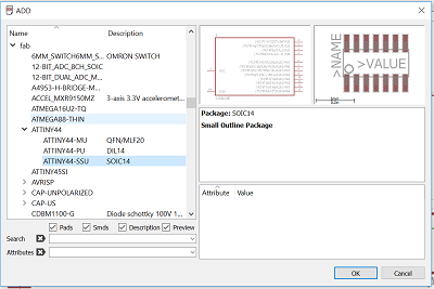
Using the PCB layout, I was able to figure out the list of electrical components and placed them on schematic layout.
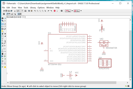
To create electrical connection between components we connect the pins with a little bit of wire and then name the pins with same names to interconnect them. .
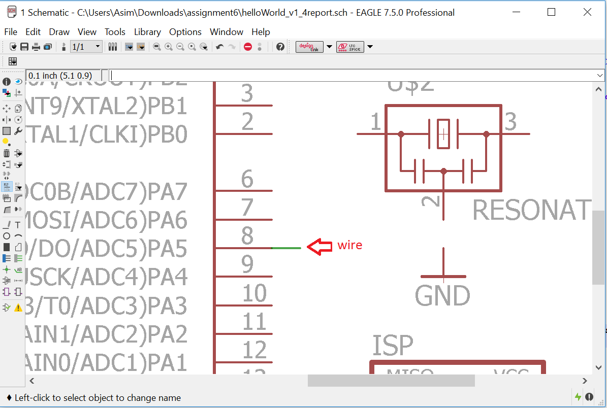
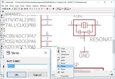
I have interconnected the pins using the naming convention convention as this reduces the chances of connection error due to wires not snapping to the pins.
This is how the electrical schematic layout looks after interconnect:
Add (at least) a button and LED (with current-limiting resistor)
For this part I have connected an LED and a tactile button to the Echo Hello World board. This is very straight forward but to make things more interesting I wanted to design a board where the pins are not necessarily locked to LED and tactile switch rather they could be connected to other Input/output devices.
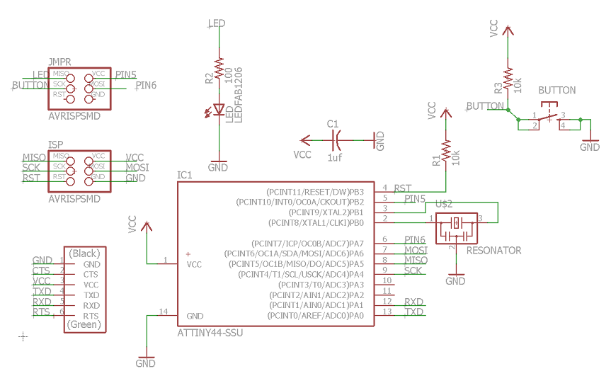
In this layout pin 5 and pin 6 are connected to LED and tactile button through ISP headers.
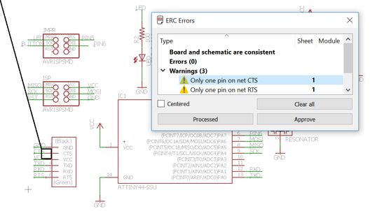
Once all components are interconnected, I ran the Electrical Rules Checks and found some warnings as some of the pins are named but not connected to any net.
Component Placement and Routing:
Now we switch to the PCB layout using schematic to board icon and we face a mess of components and interconnecting wires (ratsnet).
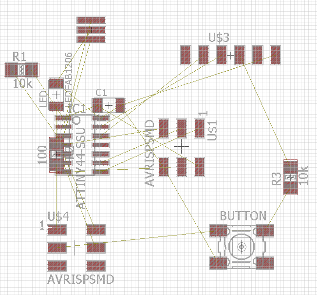
To design an optimal (in the sense of board size and complexity) it is really important to place the components thoughtfully. Although it is possible to route the traces using auto-router, however this solution is generally not the best. After several hours of trial and error I was able to make the following PCB layout.
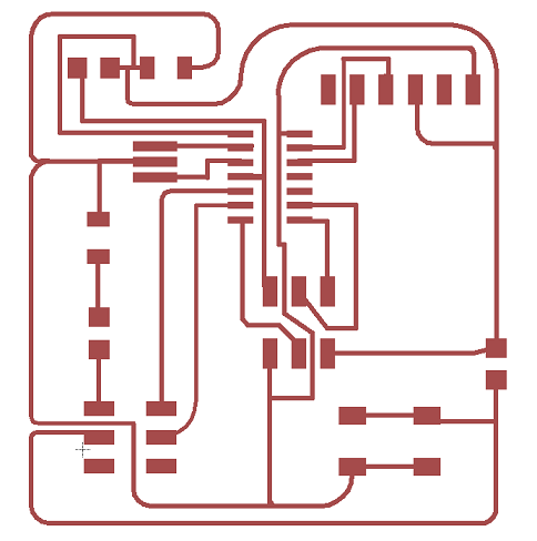
Design Rule Check and Fabrication
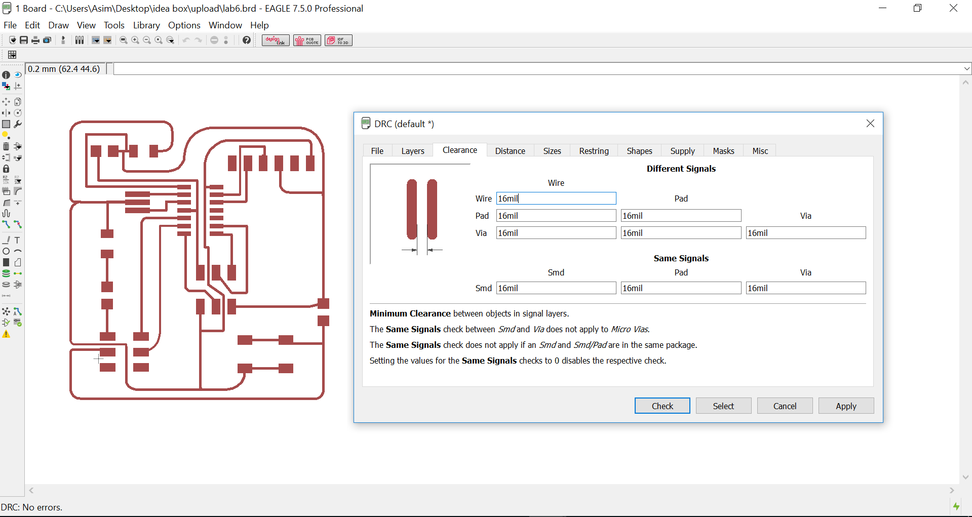
Once the design is final it is very important to test the integrity of the PCB layout using Design Rule Checks.
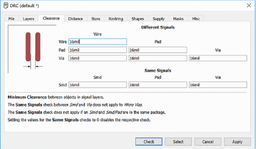
Design rule check detects possible anamolies in the circuit e.g. if PCB traces are overlapping and/or too close to each other or contact pads. Although DRC consists of a bundle of parameters but for this single layer circuit a very basic set is considered:
| wire to wire | Wire to pad | wire to via |
|---|---|---|
After completing this process I exported the PCB layout as a PNG format using File-> Export menu. We set the output pixel density to 1200 dpi.
Now we use this PNG file to generate the required code for our milling machine Roland SRM-20. The code is generated using the website Fabmodules.org.
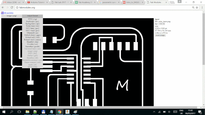
Some important design parameters (to be set in fabmodules) are:
- x0,y0 and z0 all need to be set to zero.
- home location for (x,y,z) is set to (0,0,5)
- Milling offset should be 3-4.
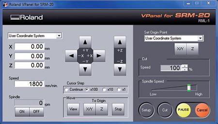
Once we had the milling machine code, we could use the vpanel software to mill the PCBs.
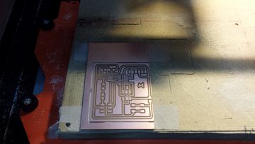
After following the straight forward procedure from assignment 4, I obtained this PCB:
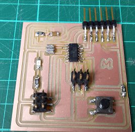
The next step was to solder the components onto the PCB. Thanks to a good practice in assignment 4 this job was pretty straight forward.
I discovered some faulty contacts with the help of Digital Multimeter and after going over the board (checking traces and contacts) with the help of schematic diagram I was able to secure all connections.
Learning Outcomes
From this extensive exercise I have come to conclude the following points.- Design of any Printed circuit board starts with selection of components appropriate for intended application. To this end datasheets must be refered.
- Electrical internconnects should be performed through naming conventions.
- Toughtful placement of components on PCB layout can reduce the size and complexity of baords.
- The DRC settings must be set in accordance with the capabilities of print mechanism. For manual design (as in our case) clearance should be kept to 16 mils.
- The resolution of the output trace images should be atleast 1200 dpi for further processing on fabmodules.org.
- Soldering of SMD components requires special attention and care. Ensure soldering iron is sufficiently hot and avoid placing lumps of solder on the pins.
- Upon completion all traces , pads and contacts must be checked with DMM to ensure connections are reliable.
Downloads
find all source files here.

This work is licensed under a Creative Commons Attribution-ShareAlike 4.0 International License
Copyright © 2017 Muhammad Asim Ali
This work is licensed under a Creative Commons Attribution-ShareAlike 4.0 International License
Copyright © 2017 Muhammad Asim Ali