Electronics Production
Objective for this module is focused on make an In-System-Programmer, a Fab-ISP. I have already made this during the one month long Pre-Academy. I first made Neil's version and then the USB key version (when I found that USB-mini cables are hard to come-by), using the components from the original board. So I'm not making another Fab ISP, but I'll modify the existing design and add more features. Also I'm thinking about exploring something new and help fellow students to make their ISP.
Since I made the board before, I'm writing about that same experience.
First lets talk about the machine we are using.
Roland MDX-20 Mill
Perhaps the most used machine in the Fablab!. This machine can be used for making the PCB (milling and drilling), carving simple 3D structures in machine wax. The machine can be considered as a mini CNC mill. The workpiece is attached on a detachable plate which moves along the Y-axis. The drilling/milling tool (end mill) or the engraving tool is attached to the head which moves along the X-axis. The end mill is attached to a DC-motor (10 W) which is mounted on a carriage that allows the the movement along the third axis, the Z-axis.
The motor (spindle) and the end mill spins at high RPM to remove the material from the workpiece as small chips. The milling bit primarily moves along the X-Y plane except for the beginning and the end of each section being milled. The end mill is designed such that it cuts into material from side, ie. the material removal happens during the lateral movement of the tool. The drilling bit has the main cutting edge at the end of the tool, which allows it to make holes in the workpiece. The tools will have flutes (spiral cut in the body of the end mill) along the length of the tool to facilitate in chip removal and sometimes to allow the flow of the coolant liquids(not for this machine) to the cutting area.

This machine has a few more tricks under it's sleeve. It can be used as a 3D scanner using an Active Piezo Sensor. The machine is capable of scanning objects at 4 to 15 mm per second
with a resolution of up to 0.05 mm. And the machine can also be used to mill soft metals like aluminum. So this machine is going to be explored further during the future
modules on 3D-printing/scanning, and CNC milling.

There are a few thing to be careful when you are using the machine
- Make sure that the Z-axis has enough room to move along z axis, else you will be left with a PCB not cut/drilled all the way or a wax model which is not complete or a PCB with copper where it is not supposed to be.
- Check the dimensions of the your original design and in the fab modules, after loading the .png. Resize if necessary.
- Also check the dimensions of the copper board being used, make sure that your design fits.
- Try to optimize your design and the placement of the PCB and origin; to reduce the wastage. If possible use the leftover from the previous milling operations.
- Use sacrificial material for PCB milling operations.
- Use proper settings and the bits, (especially, don't use the milling bit to cut, because you will break the delicate and costly milling bit. But if you use drilling bit to mill, you will only spoil the PCB, which is cheap).
- Take safety precautions, 'respect' the machine and the electricity.
Fab-ISP
The final ISP with LEDs for indicating communication and power can be found at the bottom of the page.
I made the FabISP not once but twice, first time
this one,


Now I want to talk a bit about my methods of soldering and de-soldering, it may or may not be the right way, but works best for me (may be till I see a better method from someone).
The soldering first.
Most important thing is that you need a clean surface to solder on, if the PCB is not clean enough, we have to do that first. The flux will help, but only to an extend.
The flux used in the lead-free solder is a nasty stuff and recommended NOT TO BREATH it. I use a flux pen to dispense the flux in small quantities, the flux pen has rosin
(comparatively safer, and is a natural substance) dissolved in a solvent (isopropyl alcohol). By the way, I made this mixture myself. Apply the flux only if necessary, too
much is not good. Also keep in mind that the solder wire itself has flux built into the core.
Begin the soldering from the center and move out, smaller components first. But the order is matter of personal choice, important thing is that the soldered components shouldn't hinder access to the new components being soldered. For components like SMT resistors and capacitors, start by putting a bit of solder onto one of the pad, place the component, melt the solder and align. Don't solder the other lead, not yet, you better wait till you place most of the similar components and verify once before soldering the second pads.
For ICs, I start similarly, start with soldering one pin to the pad and align the IC properly while keeping the solder melted. Once aligned, remove the iron, you are now free to solder
the remaining pins. I do drag soldering. Beginners can use the help of the solder-wick. Brush flux on all the pins of the IC, take a small piece of solder wick and wick
enough solder on it. Now drag the iron along the pins with the solder-wick between, the wick will release just the right amount of solder to the pins. The flux is used to
reduce the viscosity of the solder, to ease the flow of molten solder. Break the unwanted the solder bridges by touching up with the soldering iron or by wicking off the
excess. I prefer the biggest tip (chisel type) bit for drag soldering. And with experience you will not require the solder wick, except for touch-up.
Some may suggest against this method, saying it uses more flux and all. But I don't think so. First of all the process is quick, with experience you can solder a 64 pin
IC in less than a minute, and the excess solder applied is only very little. Also keep in mind that the flux within the lead-free solder is more hazardous than pure rosin
based flux (but cleaning maybe necessary). Also in most cases the solder used will be less, as soldering each pin one by one tends to use more solder which causes a lot
of bridging and require wicking off the excess.
By the way, I forgot to take videos of my process but this is a video that demonstrates the process of drag soldering, instead I'll show where I learned the trick from.
This one is another video demonstrating the method I use for soldering the SMT capacitor/resistor.
How to de-solder?
One can either use the heat-gun or the soldering iron to remove the components. But for the IC or any component that has more than two pins you may want to use the heat
gun.
Using the heat gun is very easy, just start it, aim it toward the component to remove (don't forget to move it around to distribute the heat, else you will burn the component
or PCB) and once the solder is melted just use the tweezers to remove the component. Applying light upward force during the process will cause the gravity to do the work.
Using the iron to remove the component is bit tricky, you need to heat both pads alternatively and as fast as possible, this will keep the solder on both the pads molten
and you can use the iron itself to push the component away.
Once again I don't have the videos of my process, so I'm embedding a video of the same process.
Programming the Fab-ISP
Basically I followed
this guide, with a minor edit, the
make fuse command is redundant,
make program does it anyways.
If all the connections are proper, and the components are all okay, the programming will be extremely easy. Like someone said "if you know what to do, its very easy". If everything works perfectly, the programing involves
- Extract the source code.
- Edit the Makefile to choose the correct IC and the clock speed ( for the one being programmed) and the programmer.
- Start clean by
make clean - Compile and generate hex code by
make hex - Run
make program(may be as root depending on the user privileges)
The Linux command
dmesg and
lsusb comes very handy during this stage.
dmesg will give some idea if the board is working or not. You will get some kernel messages when the computer detects the new hardware.
I tried Atmel ICE first, but no success. It was my first time using that hardware and was a bit complicated. Then I tried another ISP, with my friend
Yadu. Which worked just fine, I ran
make clean && make hex, which compiled the source to generate the hex code,
make program, which flashed the hex code to the chip, burned the fuse-bits and verified. Next step was to remove the jumper to disable the programming mode.
At this stage I had a working ISP, and I could see the entry (Bus 001 Device 025: ID 1781:0c9f Multiple Vendors USBtiny)
                sibu@archSSD ~ % lsusb
                Bus 004 Device 002: ID 8087:8000 Intel Corp.
                Bus 004 Device 001: ID 1d6b:0002 Linux Foundation 2.0 root hub
                Bus 003 Device 002: ID 8087:8008 Intel Corp.
                Bus 003 Device 001: ID 1d6b:0002 Linux Foundation 2.0 root hub
                Bus 002 Device 002: ID 174c:1351 ASMedia Technology Inc.
                Bus 002 Device 001: ID 1d6b:0003 Linux Foundation 3.0 root hub
                Bus 001 Device 002: ID 413c:2107 Dell Computer Corp.
                Bus 001 Device 025: ID 1781:0c9f Multiple Vendors USBtiny
                Bus 001 Device 024: ID 0bb4:0f91 HTC (High Tech Computer Corp.)
                Bus 001 Device 003: ID 046d:c077 Logitech, Inc. M105 Optical Mouse
                Bus 001 Device 001: ID 1d6b:0002 Linux Foundation 2.0 root hub
and
dmesg
[11184.067876] usb 1-6: new low-speed USB device number 26 using xhci_hcd
The ISP was tested by using the new board as a programmer to program an Arduino board I have.
Later, I moved all the components to a new board, to make the USB Key version. This board didn't work at the first time because of the loose connection, the board is very thin for a snug fit in USB port. So I made the connector area slightly thicker by applying generous amount of solder on the 4 contacts (I applied solder on the entire board too as the copper started to tarnish). Little bit of extra flux was also used to make the solder flow nicely and form a smooth profile (else the board may get stuck in the USB port). A piece of vinyl was also pasted on the backside of the board.
Mission Accomplished
Now I have a perfect little ISP of my own, and no need of any USB cables. I can now start programming new micro-controller boards, help others to give 'soul' to their own
ISPs....
ISP with LEDs
Although this works perfectively as an ISP, there are no LEDs to indicate communication. I like to have LEDs on Rx and Tx channels like the ones in an Arduino board. I found another Fabable ISP, FabTinyIsp. This has a few more features like LEDs on Rx/Tx lines to indicate communication, a reset switch, a smaller chip etc. I'm thinking about making this board, with one modification, the ISP connector to the side, the connection would be made from the side rather than top of the board. Or I will solder the ISP on the board itself and I plan for a makeshift conformal coating, using 'glue-sticks'.
Re-Designing the ISP to include LEDs
I changed my mind;
Instead of making the FabTinyISP, I decided to modify the design of the FabISP key I have made; just added two LEDs and current limiting resistors. The LEDs were added
on Rx and Tx lines, ie MISO and MOSI lines.

Eagle Files
Board SchematicI made a few changes again,
- Removed the two solder jumpers, one of the jumper supplies is for supplying power via ISP connection and I need this. Another jumper is for enabling the programmable mode of the chip, which I don't want as I have already programmed the chip and I am not intended to change it. The jumper pads are still there but not solder jumpers anymore, more like test points.
- Replaced the crystal oscillator with the resonator, effectively one component replaces three because I can lose the two capacitors connected to the crystal as well.
- Removed the .1uf capacitor in parallel with the 1uf one(between VCC and GND), the change is only 10% (within the tolerance of the capacitor?). If this is going to create any problem, I will stack this capacitor on top of the 1uf one, but I don't think its going to make any problem.
- Removed the 0ohm resistor/jumper.
The new design is here.

The short vertical bottom layer trace (blue) is not supposed to be connected, the pads are not to be drilled either. This is more like a test point, when shorted it enables the chip to programmed.
Exporting the Eagle design to .png for milling.
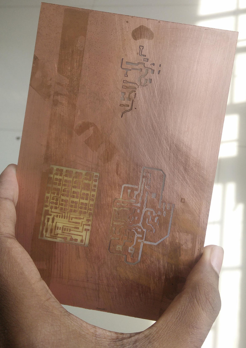
Below is gallery showing the process of exporting the image to .png files for cutting and milling traces operations.
The .png files for cutting and milling the traces are shown below. There were few mistakes and the edited images/eagle files can be found further down.


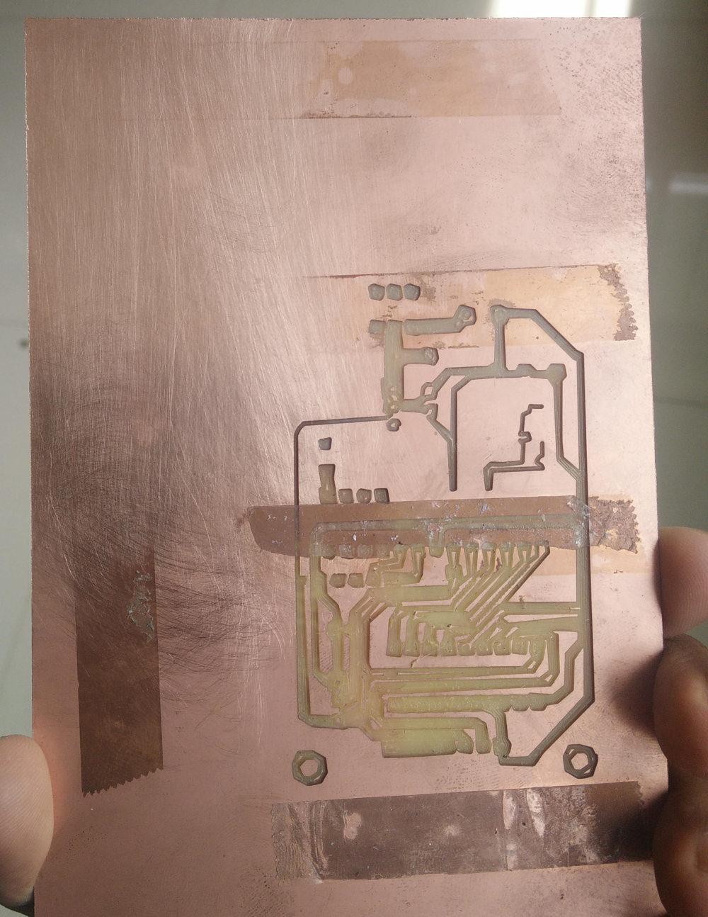
I made a few mistakes in the previous design/milling operation.
- Made holes for via(interconnect between layers) on the test pads(the pads which are to be shorted only if the chip needed programming)
- The cutout path in the milling layer was too thin, it should have been 1/32" or about 0.8mm. The result was the board won't get cut with default settings, when I forced the bit size as 0.3mm in fabmodules, the board got cut but one of the traces became too thin. Picture can be seen below.

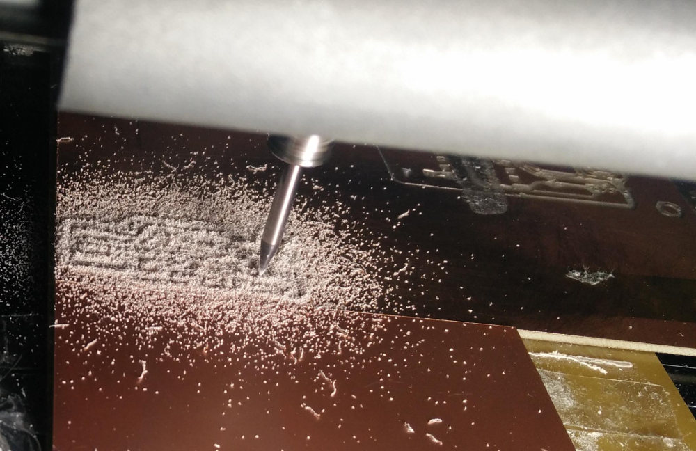
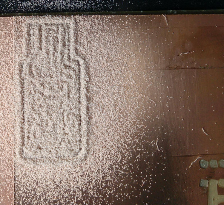


Bonus!
Here is a time lapse of the milling process, the board being milled is not mine, I just recorded it.
I used the intervalometer function in Magic Lantern firmware for the Canon 600D DSLR to take many photos of the process at regular intervals.

ffmpeg -framerate 30 -i img%03d.jpg -c:v libx264 -r 30 -pix_fmt yuv420p test.mp4
) to stitch them all into a video.


Eagle Files
for the final version go to the bottom of the page
Board-v2 Schematic-v2
Populating and Debugging


Error
There he is! I missed him so much!
The command dmesg shows the following output on plugging the device in the USB port.
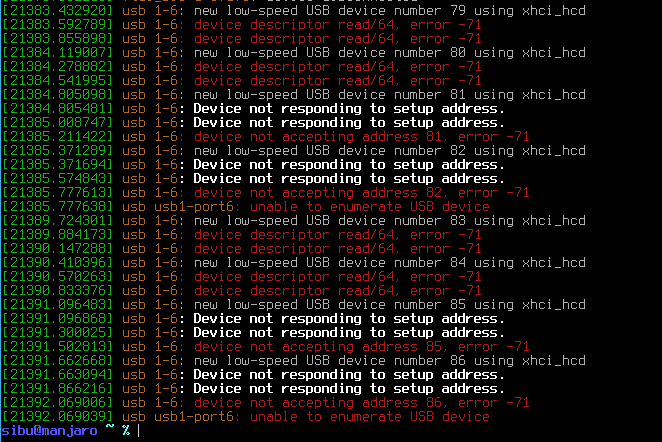
I spent some time figuring out what this error is.
- Checked the soldering: There was no issue in soldering, all the connections are proper.
- Found that this is because system detected something and the device is not behaving as a USB device should.
- First I suspected that the new LEDs were the culprit. SO I removed the current limiting resistors of the LEDs as reheating the LEDs again and again is not good. No Luck
- Used a DSO to see if I put the right resonator, I might have used 8MHz instead of 20, because I took a component which fell of from the reel, there is chance that someone took it by mistake and put it in the wrong box.
- Great!! No signal from the resonator, what could be the problem? Short circuit?
- I found the problem!
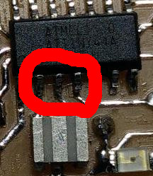
- There was thin strand of copper shorting the two pins the resonator was connected and another nearby pin to the right. This piece of copper might have came from the soldering wick during my drag soldering or from the PCB itself, the thin copper left behind by the milling process.
- After cleaning the short circuit, the PC
recognized
the board. - Soldered the Resistors back.
- The LEDs are not glowing, but this was expected as the MISO/MOSI pins are kept at a high impedance state when not in use.
- So I connected an Arduino board and tried programming it via the FabISP. Now the LEDs are lighting up, but again, only when there is data flow through the MISO/MOSI pins.
Since the board is working happily with two LEDs, I thought why not one more, a power LED, an indicator that the ISP is getting power. I didn't want to make a new board, so I just soldered
an LED and a 499 Ohm resistor to the board, between the VCC and GND.


Conformal Coating
Here is the picture of the ISP in a makeshift conformal coating. I used hot melt glue as the conformal coating, the tools used for this are the glue gun, hot air gun and 'wet finger'
to shape the softened glue. This will protect the board against the atmospheric and other elements causing corrosion, rough handling, vibrations, and short circuits from
dirt and water.

Here is the video of the new ISP in action, the board is used to program blink LED program to a 20MHz Fabduino variant I made for Electronics Design.
A snap of of the new ISP, before cleaning.
