Eagle
Our instructor led us through redesigning the Hello world Board in Eagle, Eagle is widely used and free for smaller projects. Before starting we had
to download the fablibrary (found here) so we would have all the parts in the right dimesions.I extracted the library file to my Eagle Project folder and then added it to eagle by clicking the Use Library button on the top toolbar in schematic view. I browsed to my library and clicked open.
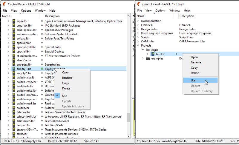
In Eagles main window there is a file browser on the left. I used that to navigate to the fablibrary wich was under Projects, and there I right clicked and selected Use, to use the library. I added one more library from the Library subfolder, the name was supply1.lbr.
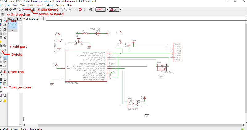
 Now in schematic view I could start Adding components by clicking Edit-> Add, or just typing Add into the command line and hitting Enter.
All of the required components where added and rotated respectivly by Right Clicking while dragging them.
Lines where then dragged to connect components, using the Original HelloWorldBoard as a reference, plus a extra button and a led that I added. Junctions can be added where lines that intersect should connect I followed instructions from the fabacademy Tutorial site to place them right. I connected those pins not by a line but by giving the pin and component a Name and a Label wich connects" them without me seeing.
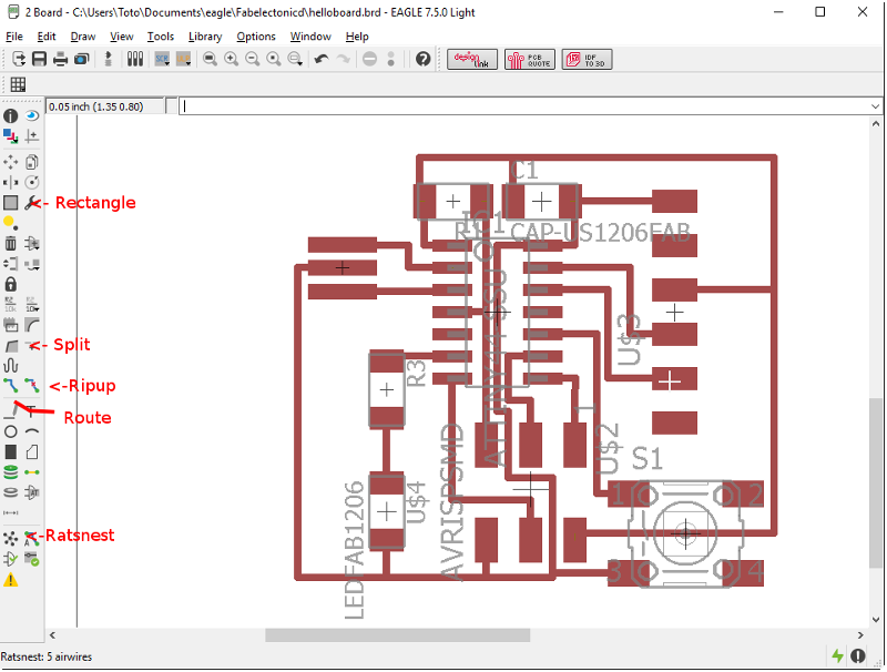
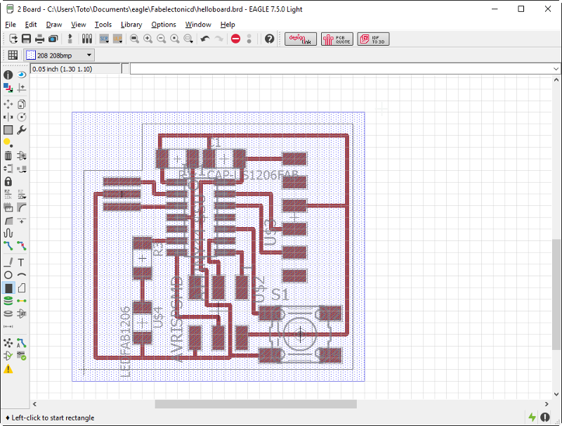
 When all components where connected I hit the Switch to Board button to go to the board editing window. There I found all of my schematic clustered up in one corner outside of the canvas but connected by thin yellow guide lines. Now I used the original Board again as a reference and arranged the components on the canvas. Now used the Route tool to manualy route the paths between components. If I needed I needed to fix any mistakes I used the Rip tool and then hit Rastnest button to calculate shortest airwires.
 When routing was complete I needed to set up and calculate the milling path for the router click: Tools -> DCR... to setup and run the test.

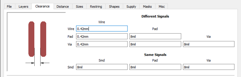
 I got some errors because the lines were space to closely together, that was higlighted in red, so I had to move the lines around to space them evenly.

I already set the alt gridsize to be 3 times smaller in the grid option, so I could hold down alt to move lines at smaller increments. But by clicking The Information button and then selecting the line I could manualy type in the x and y position of the line start and finish. When lines were nested in the center of a component I sometimes needed to use the Split tool to create a corner close to the line origin.
With all this finished I opened the Layers panel and selected the dimensions layer, on that I draged the outerboarder of the canvas to fit my pcb creation, I redrew a few lines. Then again selecting layer properties I selected another layer, in this case layer 208 for convenience. and there I used the Rectangle Tool to draw a rectangle around the design, I had it one grid unit bigger than the board. This Rectangle does not get exported but it sets the exported image size so the board layout has a border.
 I exported two images first only layer1 was showing to export the PCB paths and secondly I exported the board outline. I then choose FILE->EXPORT->IMAGE. Selected a folder and .png format with a 1500dpi and Monocrome checked.
I opened the Boarder image in Gimp and used the paint bucket tool to paint the outside rim of the pcb black.
Here is the PCB path image:
and the workfiles Schematic
Board
Milling
I ran into a few problems when milling. First I had exported an image in 150dpi instead of 15000dpi resolution and that did not work out for creating path in fabmodules.
My next problem was that I did not press the copper plate tightly enough to my wasteboard so it bulged up in the middle. resaulting in to deep milling lines.
Thirdly I inverted my boarder image in fabmodules so the tool milled the inside of my edge and ruined my paths. So I started over and milled a new board

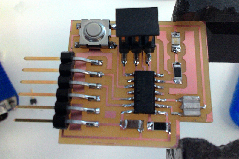
Soldering
Soldering went alright, I made a mistake placing a capacitor at the wrong place but that was quickly fixed. My microcontroler started looking like a silverlegged spider
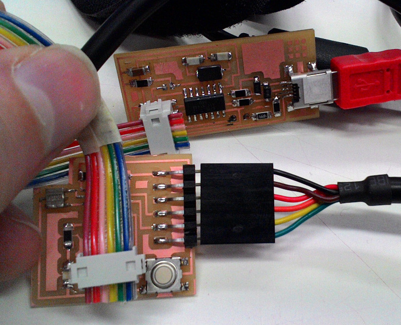
Programming
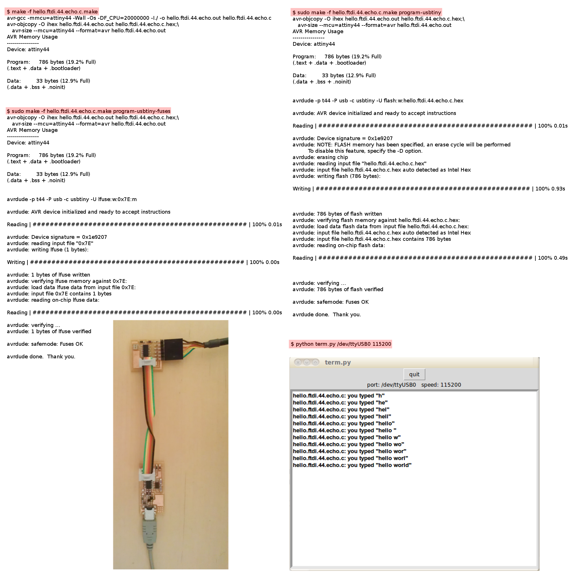
To program the Board I needed to connect my ISP board made in Week4 and to download this file and This file Into a folder on my Desktop. I then followed the code on this image to program the board. In Command prompt I navigated to my folder and the executed:
make -f hello.ftdi.44.echo.c.make
This compiles and creates a .hex file that will program the microcontroler.
and then
make -f hello.ftdi.44.echo.c.make program-usbtiny-fuses
This programs the fuses of the microcontroler to set the clock type and other function, this only needs to be done once.
At this point I got an error and my Bas my instructor pointed out that I had not connected my board to a power source. With that taken care of I repeated the last command and got an outcome as my image guide had depicted. The last line of code I ran was:
make -f hello.ftdi.44.echo.c.make program-usbtiny
This actualy programs the board.
Echo
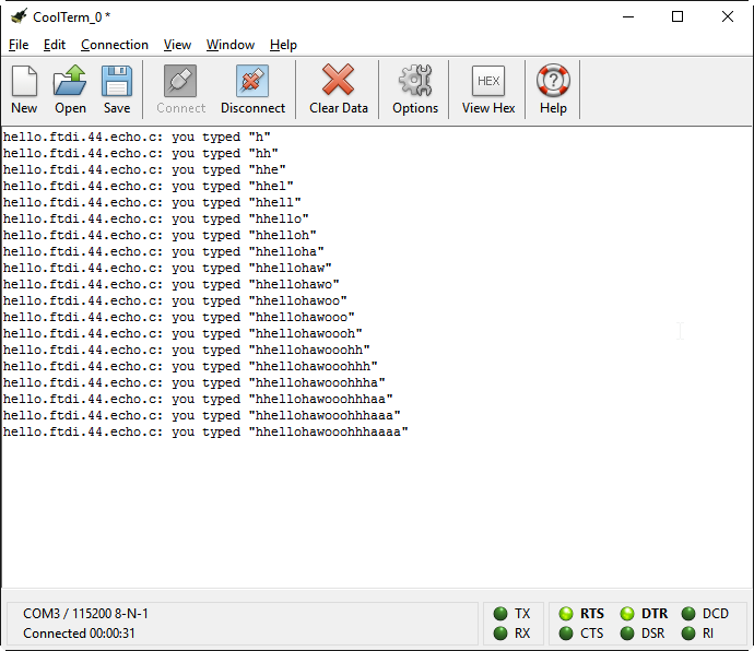
To connect to the board and test the connection I downloaded and installed CoolTerm I clicked options and set Baudrate to 115200, and Port to COM3, I knew it was COM3 because I checked the board properties in Device Manager. I then clicked Connect to connect to the board, I communication terminal opens up that returns the characters I entered up up to a certain count.
kicad
I started a tutorial on the open source program KiCad I got as far placing components in schematic view before I ran out of time but I must say its UI looked good and I felt just about as comfortable using it as in Eagle, I could well imagine it as my pcb program of choice.