Two steps forward!!!!
Electronic design is fun! No, really, it is. Ok, it's a bit frustrating. Yes, it can be very frustrating. But when it works, how cool is that! So that is about how the week went for me. I'll get into all the mind-numbing details later but suffice it to say - I learning a lot this week but it was very frustrating. I'm going to do my best to document the gory details because it really is in the details - and I mean the 1/1000 of an inch details - that this week proved to be very instructive. Plus some interesting observations on pcb and schematic design. If you are still interested, have look at the page for Electronic Design since I'll be drawing a lot on information assimilated during that week.
Where we last left off...
In electronic product, there were quite a few issues with getting the self designed board into a state where CopperCad (CC) would show a proper output. In fact, we were never able to get a proper ouput based on the circuit designed usign EasyEDA. There was a lot of back-and-forth questioning the potential origin(s) of the problem. So this starts with those issues and moves forward. Instead of starting with the AVR ATTINY44, the ATMEGA328 will be used instead. This is a more sophisticated chip with more IO and additional functionality including built in A/D converters. It also comes in the 32 pin TQFP package which is a bit of a challange due to the small pitch.

Designing the schematic
I'm continuing to use EasyEDA since the more I learn about it the more I like it. One of the first things to do is find the components we'll be using. One thing about EasyEDA is the component libraries are reasonably large but not so large as to be unmanageable. There were about a half dozen version of the ATmega328 and one that had the appropriate foot print for the schematic. Its important to try and find the correct component/foot print match though in some cases substitutions can be made or slight design changes.
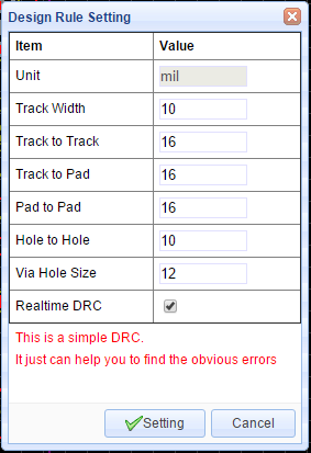
The track width was set to 10mils since this is about the lower limit for milling to still have a solid surface attachment of the trace.
One element that makes schemtatics much easier to read are NetLabels. These keep the designs from having connections running everywhere and make it much more readabilty. Don't despair, there will be many opportunities to make connections when it comes time to design the PCB.
Finally, when building the schematic keep in mind how the connectors are wired. Before wiring together connectors look at the physical layout of the chip. It doesn't always make sense to wire together one port to one set of pins. From a layout perspective, sometimes it is better to mix and match to facilitate routing espeicially since we are working on single sided boards.
Designing the PCB
One thing that is important to note especially for online sites, is how frequently settings are designed to run on industrial photo-lithography equipement. The resolution of such machine is mich higher then our much loved 1/64" bits so if these out-of-box settings are used, the cut path software will produce erronous output (which you may or may not immediately recognize - especially if high density or large PCB boards are being designed).
Most PCB layout software has some sort of design rule manager which permits defining a set of constraints applied to the traces and pads. This is ESSENTIAL in designing the boards since it provides immediate feedback concerning the positioning traces and pads. The image shows the settings for EasyEDA that permit Coppercam to correctly route the board with the 1/64 bit. If the design rules are not respected it is almost certain there will be shorts in the boards.
One problem I initially had was wanting to use the Auto-router functionality. Auto routing produces a very nice set of traces once the position of the components have been fixed. But there are two major problems - (1) auto-routing - for the case of EasyEDA - assumed that boards would be build two sided and got itself out of single-sided routing constraints by using vias on the bottom of the board and (2) once the correct design rules were applied, the auto-router was not able to find a solution for the board.
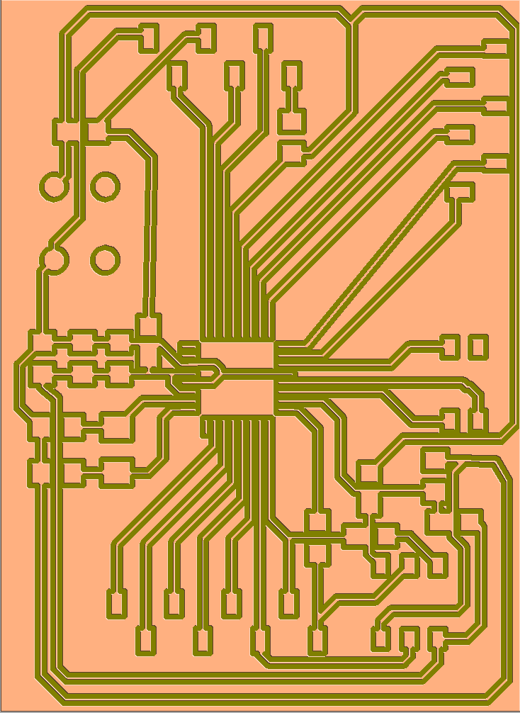
To get around the issues, I finally used hand routing which ended up not being as horrific as I thought if one (a) respects the design constraints imposed by the bit size and (2) pays careful attention to how the chip is layed out and makes schematic changes to ensure large board items like headers are linked appropriately. With all this in mind - and the occasional use of Ok resistors as jumpers over certain traces- I was able to come up with a board design that could be milled without errors.
CopperCAM is your friend, really!
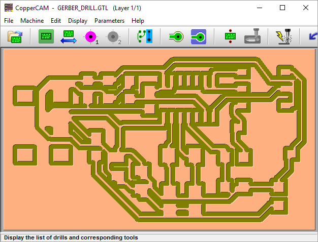
CooperCAM is the software translates the Gerber input into the cutpath for the Milling Machine. The set of images on the left illustrate the output of CC both in terms of cutpath and the actual copper output which is computationally rendered. The images are clickable if you need to see them in greater detail. If one looks closely it is obvious there are areas where copper traces and pad overlap which would cause a short circuit. Both the sets of output illustrate this problem. So as they say in IT - "Garbage In/Garbage Out".
Going back to EasyEDA, the Design Rule analyer showed several errors where traces were too close. The errors outlined above were already outlined by the design software, it was ignored by the user which proved to be a fatal oversight. Going back to EE and taking the snap-to-grid down to a single mil, it was possible to move the traces to be exactly between the pads which removed the error. The other error required the ATMega pads to be reduced from the normal size to the width of the lead - Neal even mentioned this in class which is how I found the solution.
Getting a millable cutpath requires - first and foremost - that the design softare has the correct design rules for the type of construction that will be implemented for the physical board. This data needs to be accurate to the mil or else the milled card will present errors. The design rules used for this example are shown in the image in the previous section.
Mill baby, mill!
Finally the output was 'clean'. The images on the left show the output which is of a slightly earlier version that still presented some errors but addressed the issue referred to in the previous paragrpah.
Unfortunately, the milling process abruptly stopped on two occasions, each in a different section of the board and we are in contact with Roland to try and ascertain the origin of this issue...
In fact, it turned out to be something simple! CC has a limit on the number of traces that can isolated with the free version and the board was several traces over the limit. Since we generated milling files from two different machines, the G-code order was not identical so the milling stopped in different places. I will let CC know what it would be helpful to generate an error/warning message when a file is saved that exceeds the number of free traces and that the milling will be incomplete.
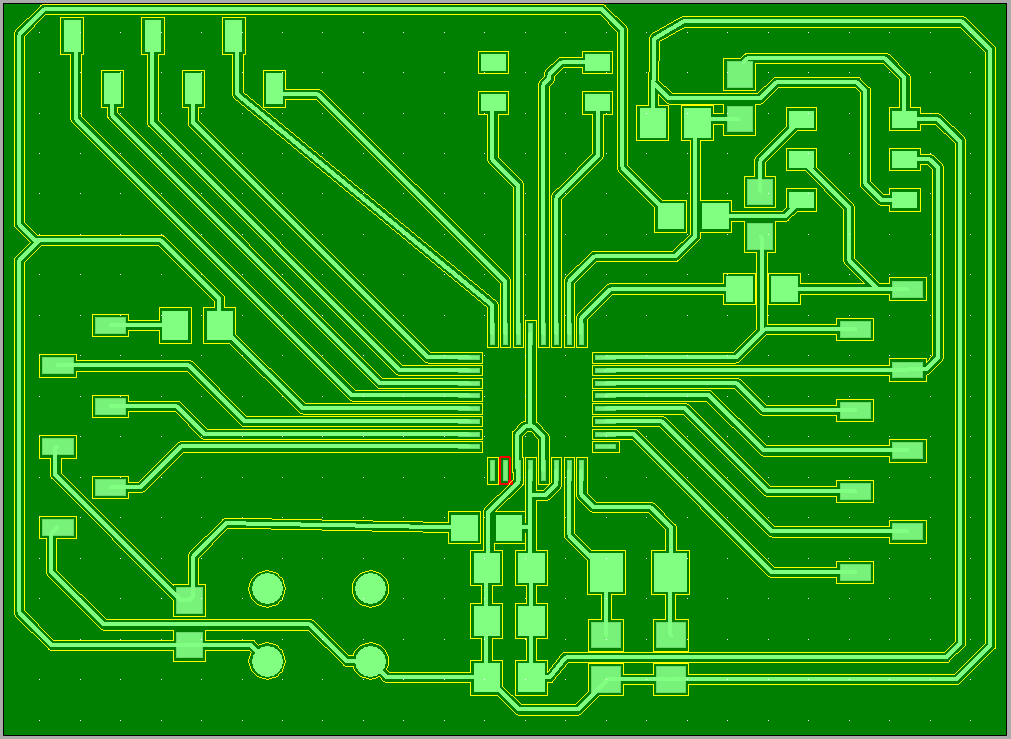
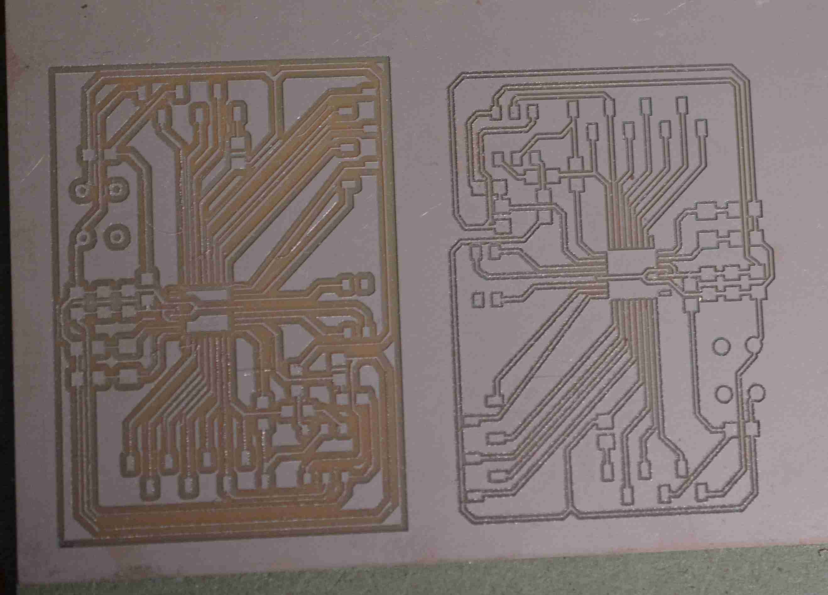
As a plan B, we used Fabmodules with an SVG output from the EasyEDA and the difference between the two is shown in the picture on the right - Fabmodules on the left, CC on the right.
In any case, we are able to mill a reasonably high quality board that can be soldered. Remember to sand down the surface of the board to remove any burrs, blow it clean with compressed air and do a visual inspection with a good jewelers loop to ensure traces are clean. I also do an isolation test to ensure there are no shorts due to copper fragments wedged in the traces.
Stuffing the Board!
Stuffing the board turned out to be relatively straight forward. I'm using solder-paste and hot-air since I find this a more efficient way to get the small SMD components on the board. The soldering-iron is very using for cleaning any bridging between the pins of the micro-controller. Continual continutity testing also helps to ensure there are no 'hidden' shorts underneath hidden traces. Since 0K resistors were used on several occasions to bridge traces it was important to test isolation was clean since things are very tight.
There were two design issues with the board. One was the wiring on the switch. The ratlines generated in EE were not inline with the internal wiring of the pushbutton switch. This will require a redesign/remilling of the board to correct, but is not technically show-stopper since the button is just to reset the chip. The second design issue was the use of a 20 Mhz crystal. This was problematic since the ATMega 328p is designed to run at 20Mhz but requires some modifications of the boot loader. We are in the process of trying this out at the moment but are having an issue with the ISP bootloader and drivers.
Meanwhile, I need to go back and make those corrections to the board and re-mill.
To-do
While Fab Academy is very SMD based oriented, it would be good to some experience using through hole parts. This requries using the drilling files but it appears to be relatively straightforward.
Bibliography
This article discusses in great detail PCB milling with loads of information on V-engravers.
http://www.precisebits.com/tutorials/pcb_mech_etch.htm http://www.uddeholm.com/files/Cutting_Data_Corrax_eng.pdf http://www.precisebits.com/tutorials/calibrating_feeds_n_speeds.htm