Electronics Production
One significant issue in doing any electronic assembly project is choosing the proper design tool. The tool needs to have a several core functionalities. This paragraph is just to share my frustration with how difficult current open-source solutions are to use. We were trying to build the FabISP kit from scratch based on the existing schematics and have not found a solution that could be called efficient. The most significant issue has been having a component library containing the components used in the circuit. Everything evaluated including PCBWeb (Digikey), Circuit Maker and Kicad all seem to be lacking in one component or the other. Even in the generic parts library there weren't even generic footprints. Then there are products that force you to share your design with everyone. While not all free products were tests, many comments appear on the web around products that don't permit Gerber export, only allow a very limited number of components, tie you into a single supplier. This web page is a good starting point and make sure to read the comments. From the bowels of that page I did find EasyEDA which is web based design product which seems to address many of the faults of the other units. We shall see...
Later in the day...
OK, to sum up our experience so far - one step forward, two steps back. EasyEDA cranked out great schematics and the more I use the software the more I like it, except...
Let's take a moment to talk about what I now discovered is called the 'Toolchain'. Much like a 'Ball-and-Chain', this terms refers to how only a set of restricted pieces of software work together to actually get the needed output. EasyEDA provided a number of output formats including - SVG, PDB, PNG and Gerber.
And now it all goes wrong!
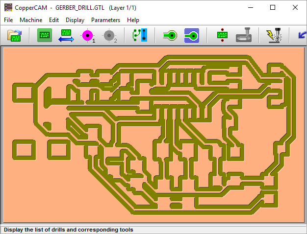
We found the software CopperCAM to be interesting so we were going to use that the generate the cut-path and send the output into the Roland. When we input the Gerber file (w/ GTL suffix) into CopperCAM we get the output you see at the right. Ouch! This was unexpected and represents, what in is France is generally referred to as 'La merde'. Notice first that no individual pads are present where the USB connector is placed. Traces seem to overlap, jumpers are missing separation spaces. Basically, this board would be worthless if milled. So what's happening?
Could it be the EDA?
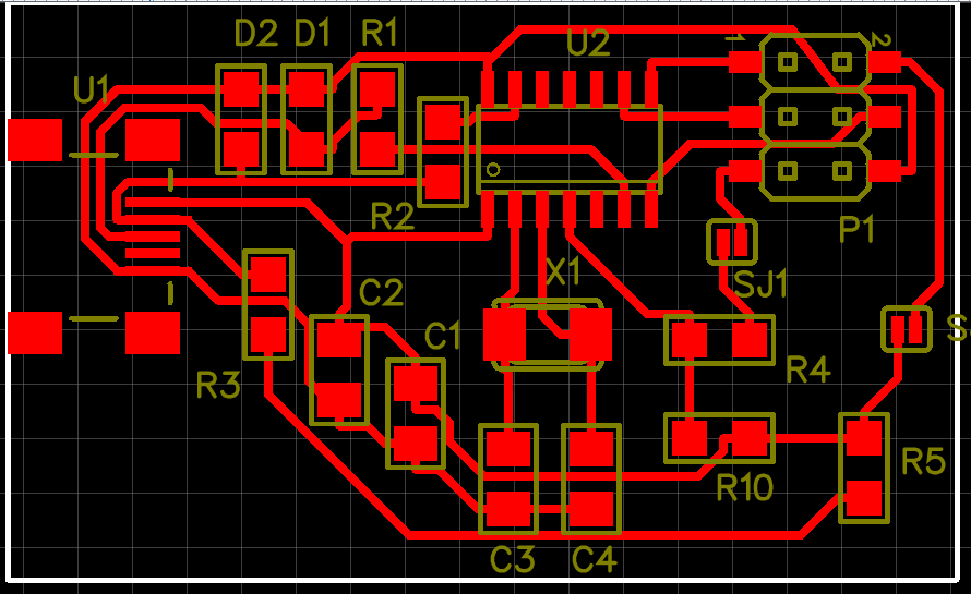
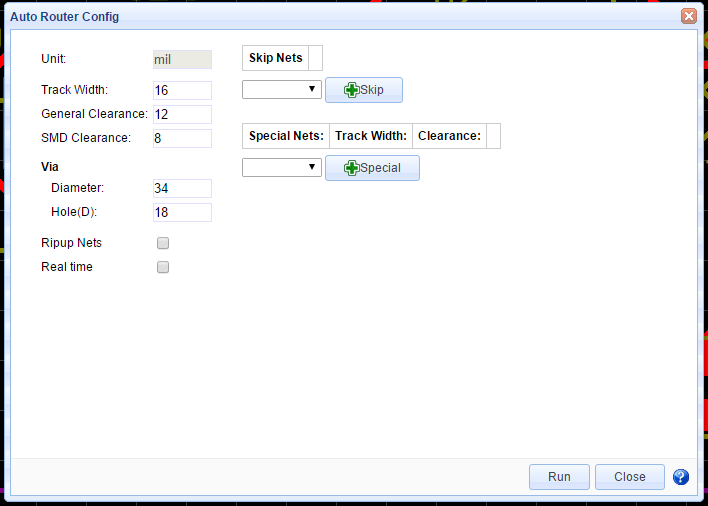
On the upper-left is the routing path calculated by EasyEDN. Note that to achieve this routing path the parameters are those listed in the image on the lower-left. It took quite some time to get the routing to not require any vias on the underside of the board. There was quite a bit of trial-and-error involved in positioning the different components. Placement and routing are hopefully subjects that can be explored in greater detail much later as it seems to be an element of circuit design that is quite difficult even for the computers.
Before going further, we are going to ass-u-me that the output of the EasyEDA software is correct and conforms to norms. There is some reason to believe this may not necessarily be the case given certain things we observed when using the Fab Modules; however, this could also be related to Fab Modules. We simply don't have enough time to investigate the origin of the discrepancies observed. I may integrate this information another time as it is quit interesting to see how "standard " file formats may not be so standard.
Could it be CopperCAM?
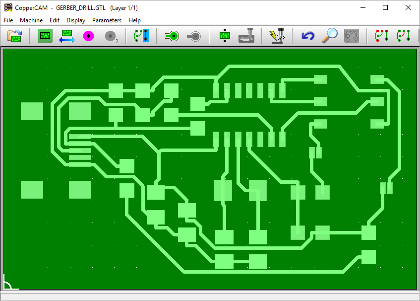
On the right is the Gerber file input displayed in CC. Note that all appears to be identical to the what was displayed in EE so the data is being transferred correctly. So the input data looks good and CC can read the file correctly. The CC documentation is lacking in details and it seems that CC requires the Gerber input as primary data source for cutpaths. This is different from the Fab Modules that permit multiple input types especially graphic files. While CC does except different input files, we observed some behavior that could be not be explained via the documentation.
Further investigation on the internet of other CC users turned up some configuration differences in the tools. Perhaps this is a more fruitful path of investigation.
What about the bits?
The 'standard' bit used for milling in the Fab Academy is the 1/64(0.015) inch ball-nose or square-end endmill. This translates to slightly less then 0.4mm or 40 mils of width. In the previous section, the general clearance in EasyEDA was set to 12 mil and SMD clearance was 8 mils (NB - Why there is a different clearance for SMD, I have no idea). So, already there is an issue between the computer generated clearances and those imposed by physical limits of the tool. And here is the question - how to generate efficient traces without resorting to vias?
One tool that hasn't been mentioned is the V-engraver which is a 'V' tipped tool. These tools permit drilling much 'thinner' channels between traces but are more complex to manage since the width of the cut is dependent on the depth. This can become an issue when the board to be milled is not 'level' within the tolerances of the tool. Any warping will result in inconsistent spacing potentially cutting traces or created separations that permit bridging. Theses tools are generally more fragile then end-mills (yes, you read that correctly - even more fragile). Luckily the price is lower; however, word on the street is quality can be very different depending on manufacturer. We place an ordered to see how these tools function in comparison to endmills. Stay tuned!
UPDATE! - We've doing some tests using V-type engraver and initial results are interesting. First, the traces cannot be nearly as fine as when using the endmill. However, having said that the isolation paths between traces can be much thinner. So, traces end up wider while isolation paths are thinner. Second, attention needs to be given to pad spacing. As an example, the stand pad width for the ATMEGA package needed to be reduced when using an end-mill to ensure the bit could pass between the traces. With the smaller isolation paths this is no longer necessary and even counterproductive since a spot of copper is left between the two traces which creates the risk of shorts. In any case, further investigation is necessary but initial results are promising and more effort in this direction could be productive.
The end!
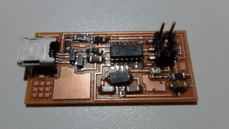
To complete this week's lecture, we still needed to produce the FabISP, so I gave in and used the stock PNG and Fabmodules. Machining was flawless on the Roland MD-40 and it was relatively straightforward to solder together the board. I'd never worked with 1206 SMD components and realized that both my vision and hands were not what they were only a few years ago. I will not go into solder paste and reflow this week but suffice it to say that I will be looking forward to employing more 'advanced' technologies to overcome my physical limits! I admit I did use the hot-air station to get me out of some sloppy soldering jams. Even Lorenzo was impressed with the abilities of hot-air rework stations.
Unfortunately, the board programmed well but was not being recognized as the FabISP board by my windows machines. Some hardware debugging showed some incorrect resistors - when it says 100 you shouldn't ignore the little 'k' at the end! But I found my favorite jeweler's loupe and reviewed SMD resistor labels so it was another 'learning moment'. Someone needs to explain to me why SMD capacitors have no capacitance labels as this is going to be a pain later. The week finished with a working FabISP and a few more grey hairs for Lorenzo.
To-do
Investigate the abilities of the Roland to do 'Auto-Z' leveling. It is possible in some software to probe the surface and build a 'map' of the surface the machine can use to adjust the Z-offset on the file. This is of particular interest when running very fine V-tips. We have a the touch scanning attachment for the Roland so it will be interesting to see if the technology is already integrated.
I've also found a YouTube page that shows double sided milling of PCBs using V-engravers and FR4 boards. This is interesting not only for the use of v-tips and double sided copper but the fact it was FR4 (fiberglass) PCB board - and the bit speed was very fast. All-in-all in excellent video to watch.
Bibliography
This article discusses in great detail PCB milling with loads of information on V-engravers.