Now Design your own PCB!!
Circuit board design with Eagle
From last 'Electronic Production' assignment, I had already Eagle on my laptop.
So I just stuck to it rather than using other software.
To make a Schematic, I simply adjusted the schematic file from
echo hello-word board example,
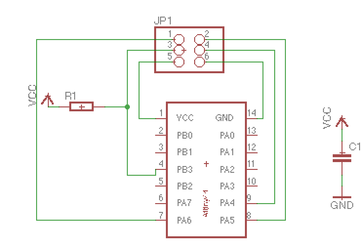
by adding a switch, a 2x6 pin header for extension and 2 more resistors to it. I added a pin header instead of an LED because I wanted to have a versitile board where I can still access the pins of the attiny such that I can play around with it and learn about the functionality. I used LED in the board for communication in Week 15 which I used in a video in Week 16.
HOW TO: Schematic Design
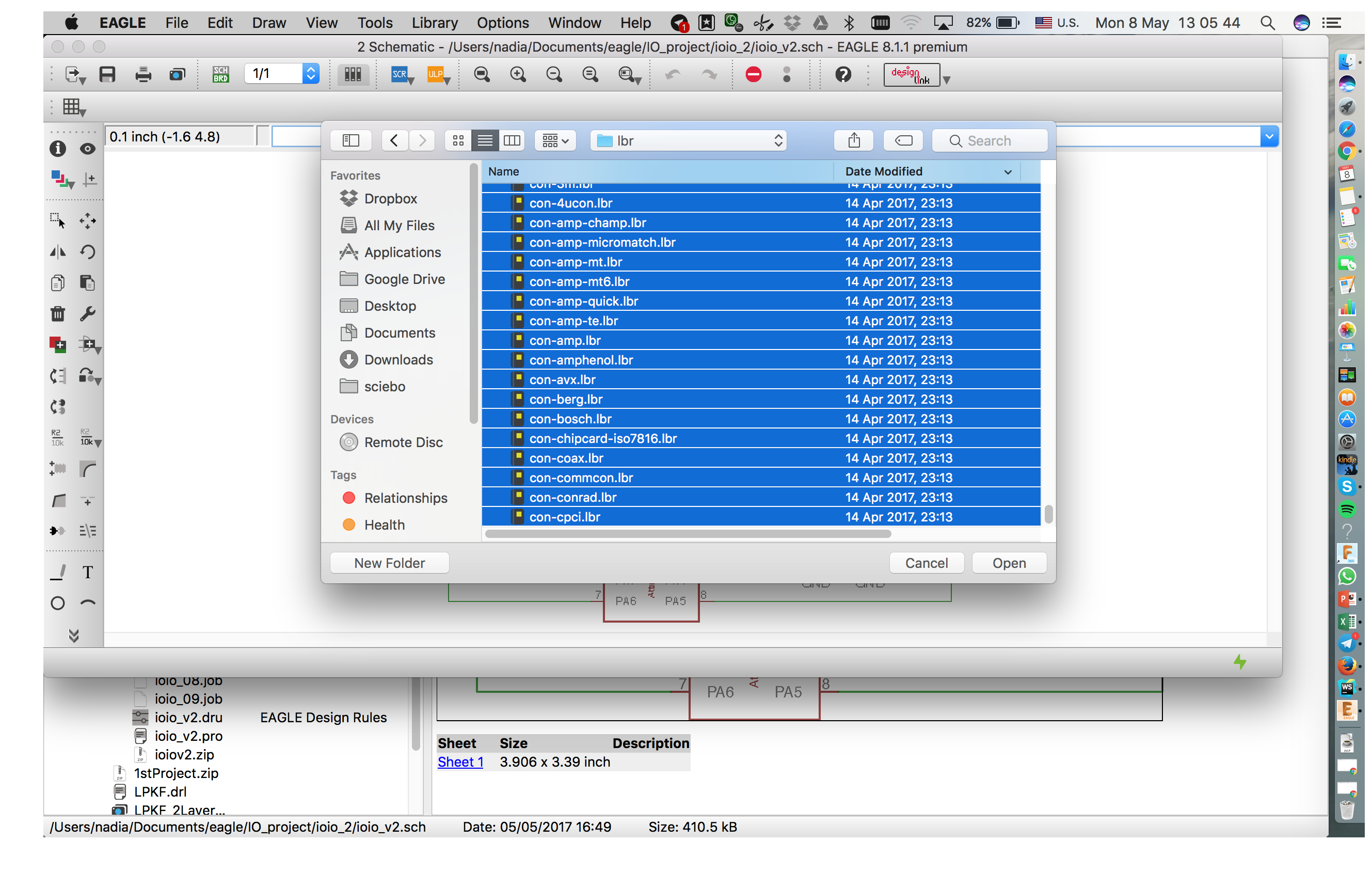
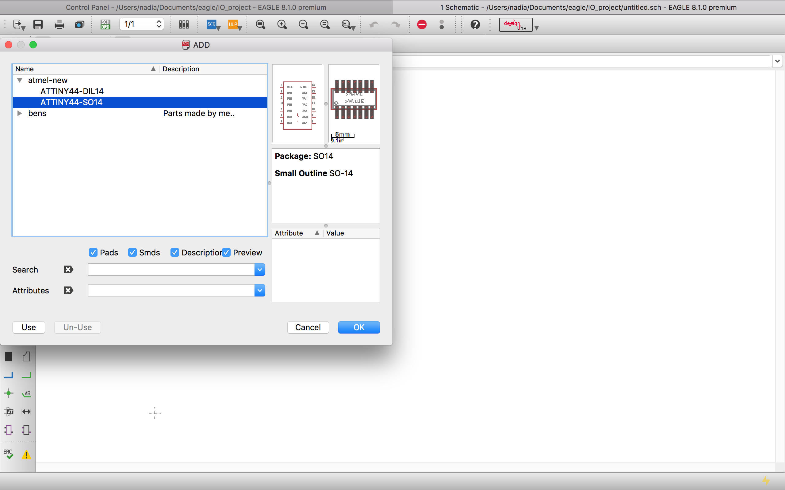
- Include all the libraries in Eagle using 'use Library' from upper panel.
- Add the necessary components to the board.
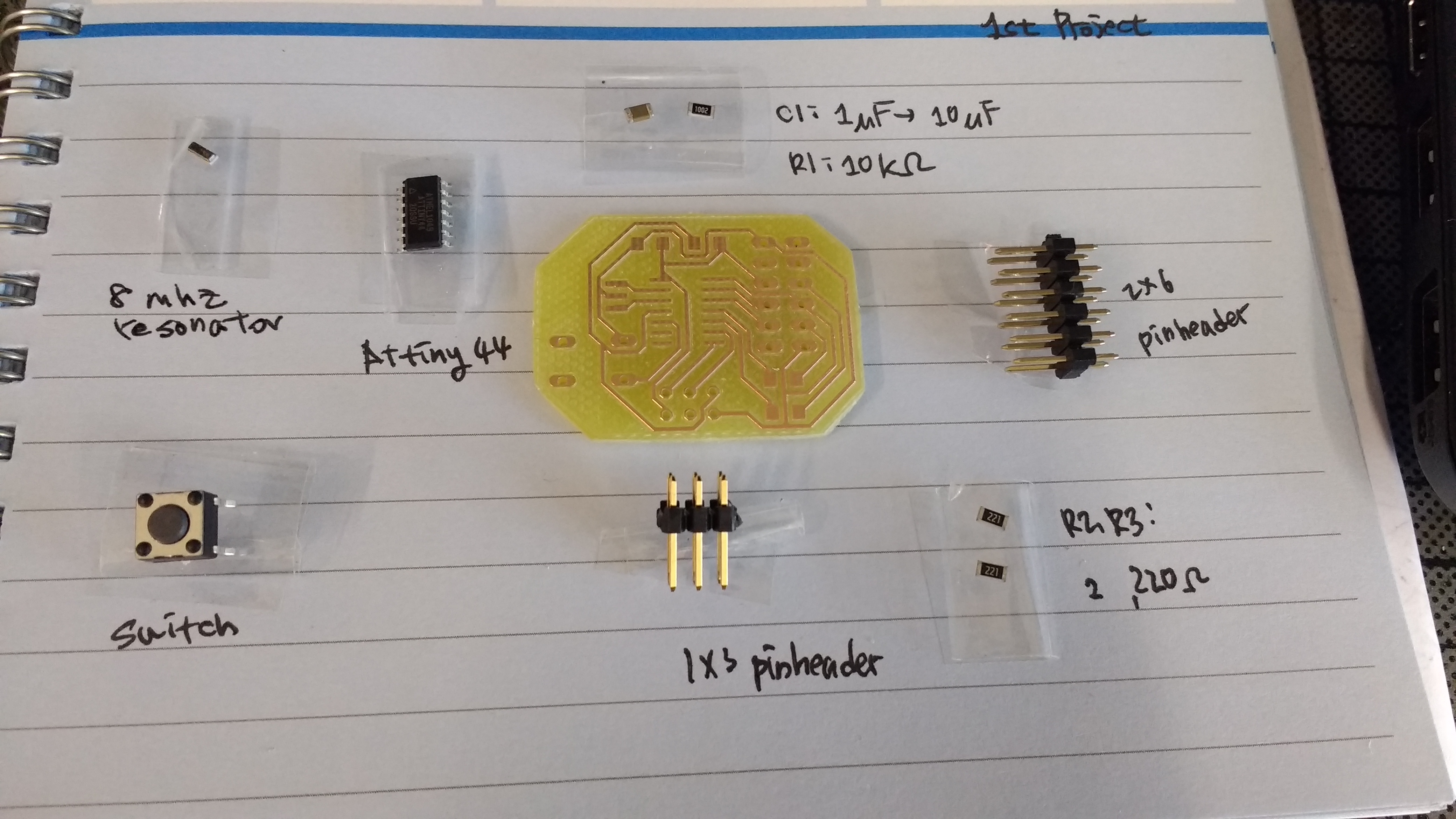
Components to be added to a circuit, and where to find in the schematic library described below:- Download Attiny Eagle library
- ATtiny44 microcontroller, you can find it under 'atmel-new' > 'ATTINY44-SO14'
- 1 capacitor, 'C1206' > 'C-EUC1206 (C-EU)' *(C1-1µF)
- 3 resistors, 'R1206' > 'R-EU_R1206 (R-EU)' *(R1-10kΩ, R2-220Ω, R3- 220Ω)
- 2 1x6 PINHEADER, 'PINHD 1x6' > 1x6
- 1 2x3 PINHEADER, 'PINHD 2x3' > 2x3
- 1 Resonator, 'CSTCR6M00G53Z (CSTCR)'
- 1 Switch
- Connect parts such as a sample schematics.
- Connect rest of the parts(Resonator, Switch, 2 Resistors, and a Pin header) to a schematics
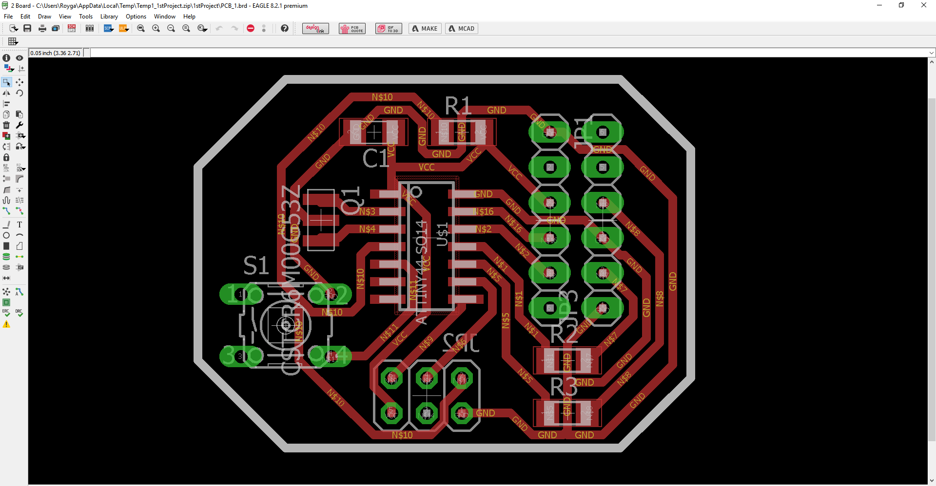
Board design with Eagle
To make a board, i had to
For me (manuel) routing was really a puzzling process, and it took me really a long time.
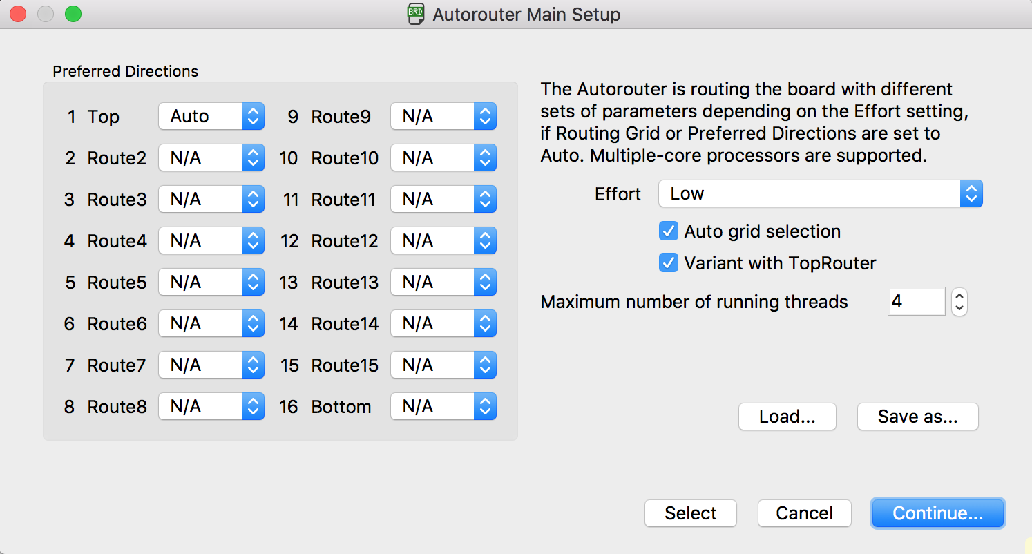
Then 'autoRouting' function provided in Eagle was real life saver.
It is also possible to mix manuel routing and autoRouting process, which is to
HOW TO: Board Design
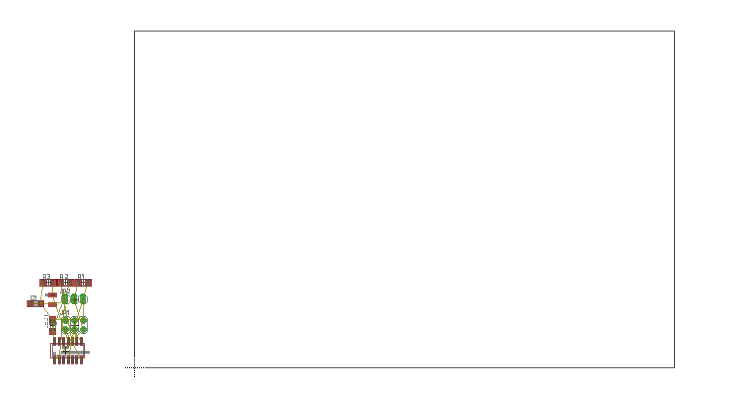
- Create .brd file from the schematic, as board is created outside of the working place(inside the line) you can either move the entire board inside the outline(which I chose to do) or delete the outline.
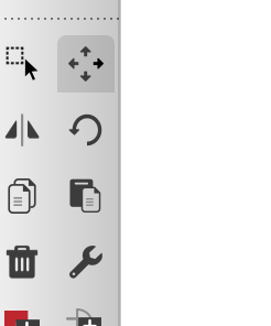
- Route the board, tools for routing can be found from the left panel of the screen.('Route'or AutoRoute')
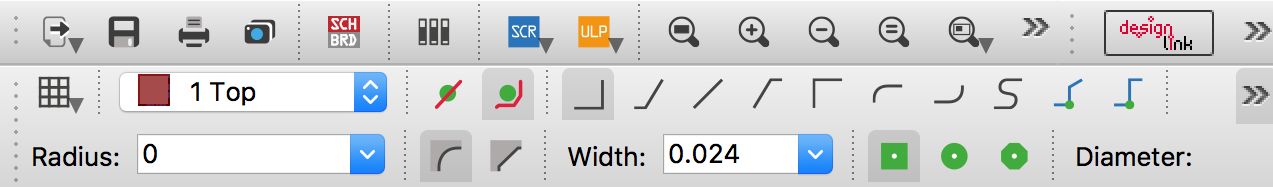
- Be sure to adjust line width to 0.024(from 0.016 as default) and line is selected to '1Top'.
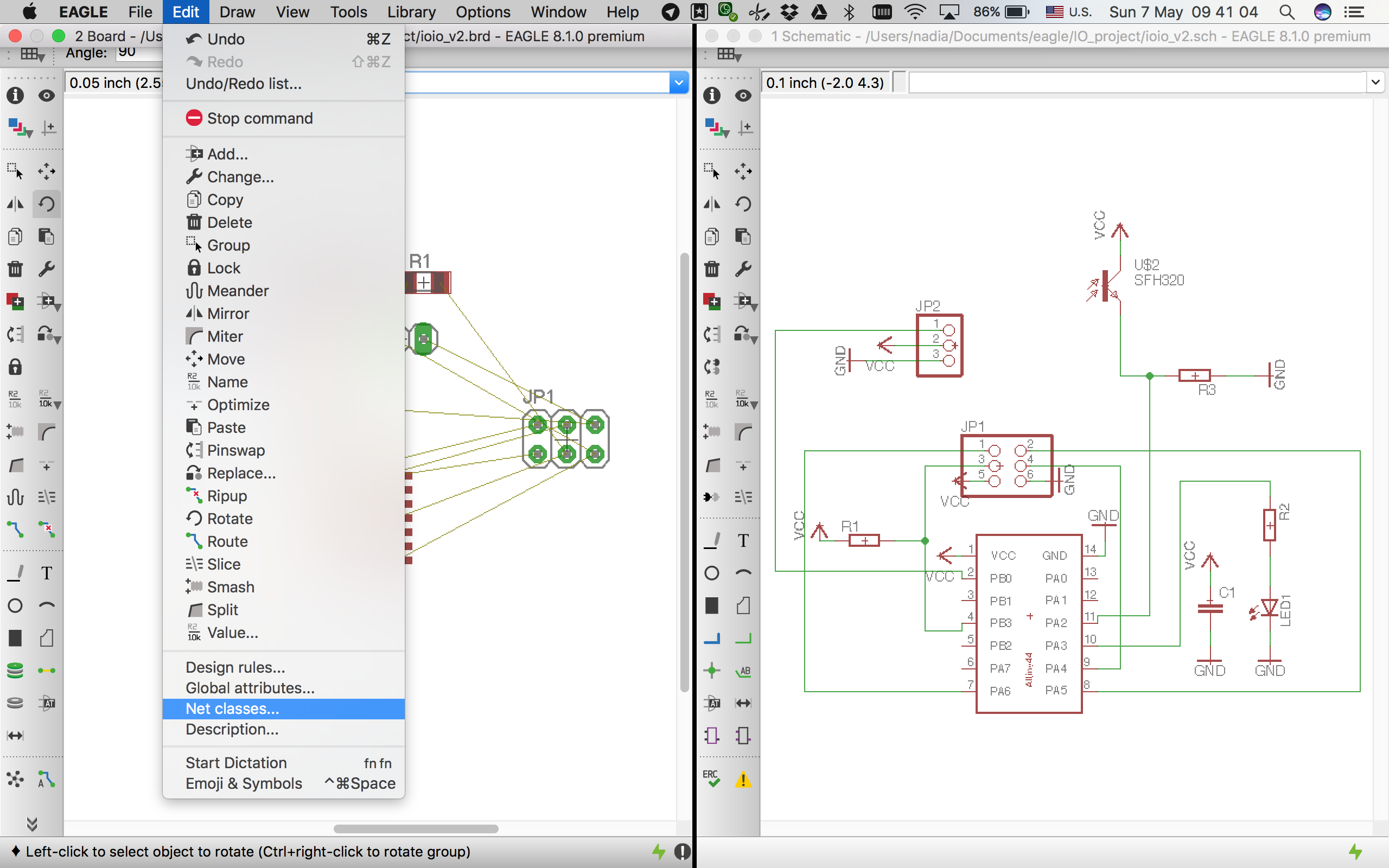
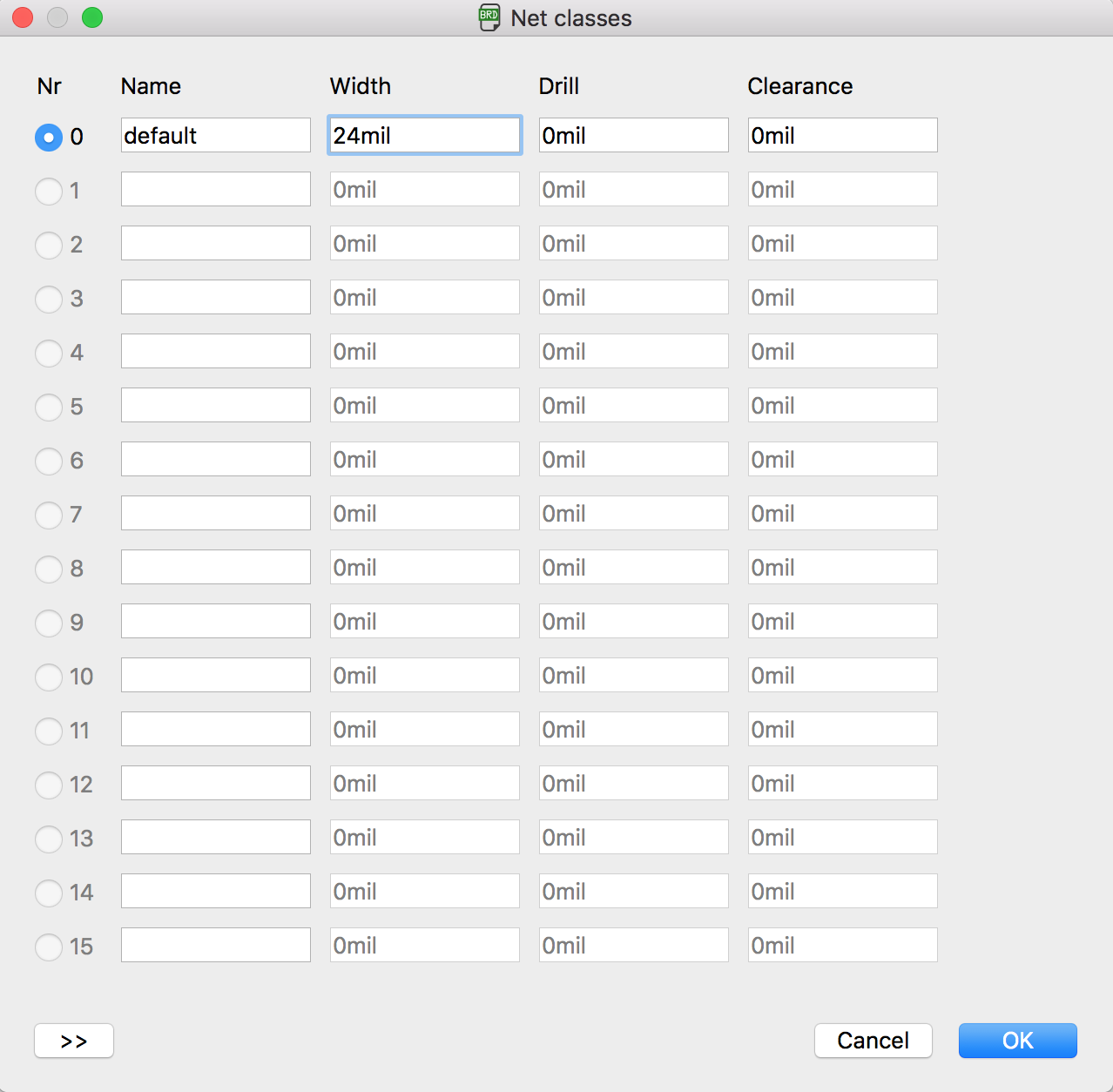
- In case of 'Autorouting', you can adjust width of entire routing line in Edit > NetClasses.
- Create outline
- Select Line tool from left panel.
- Select layer as '20 Demension' from panel above.
- Draw outline close to the circuit(save space- economical reason) with the line tool.
.png)
Final check(optional): Checking Design Rules for milling and soldering
I found following series of articles on using Eagle from Sparkfun
really helpful as a novice user.
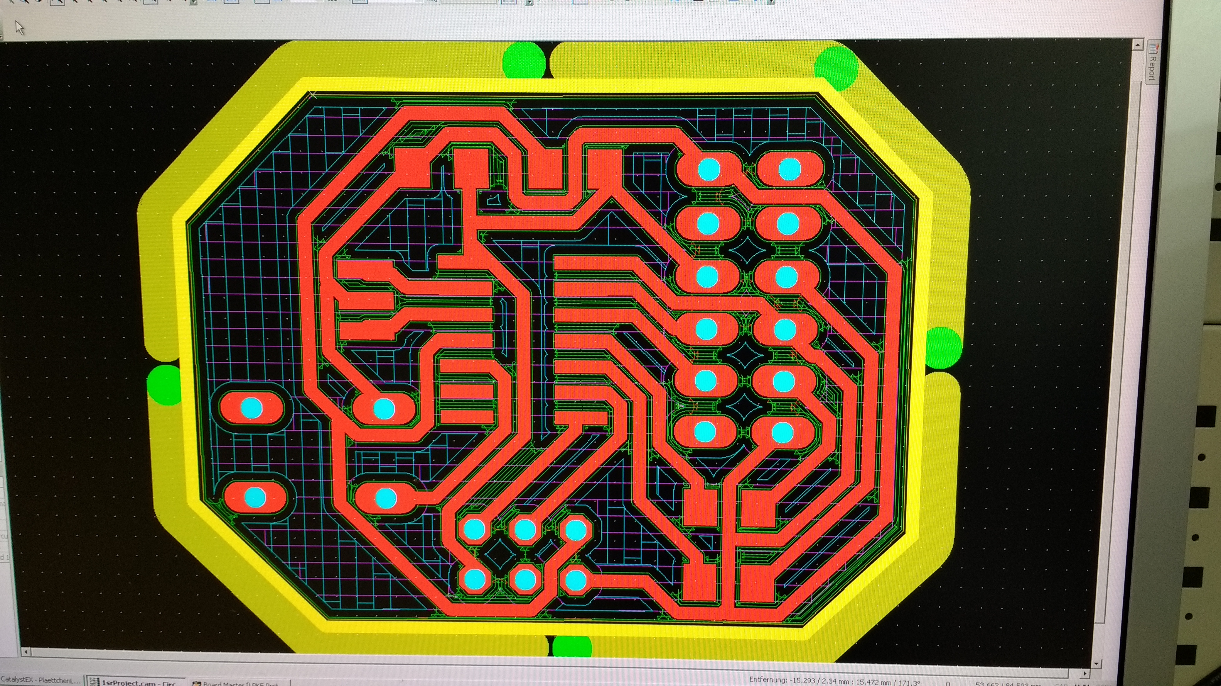
According to the series, before creating Gerber files, it is a good practice to check whether routing you made inside the board is not violating the basics rule such
as clearance(enough gap between traces), overlap(if two signal traces are overlapping) and will at the end work.
It also provides pre-made design rule they have already generated. After you load and check your board with provided .drc file and get "DRC: No Error" message, then you are good to go.
If not you will have to adjust your board. My first board passed successfully in this step.
Apart from this, I have also learned from our instructor Marcel that I need to think ahead of milling and soldering parts in design step itself.
- Having wider routing lines when creating board makes your soldering process lot much easier.
- Try to avoid the situation where lines get too close to each other or go underneath of other components(Hard to solder)
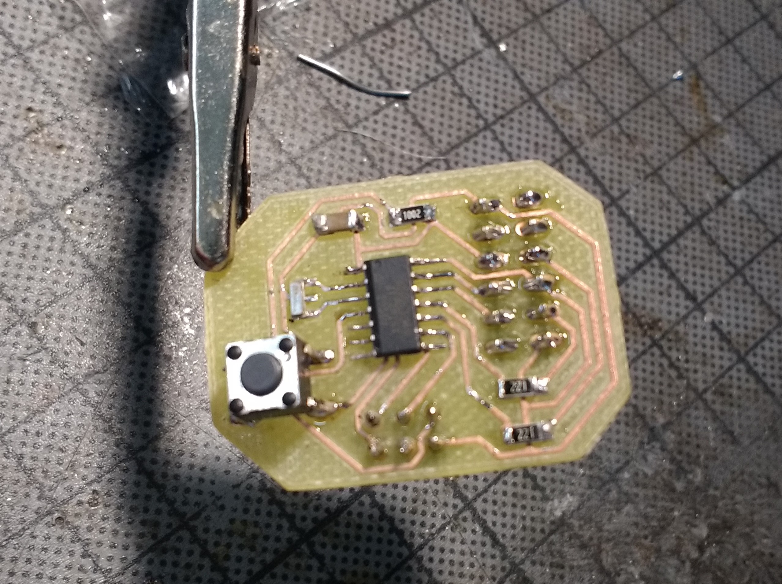
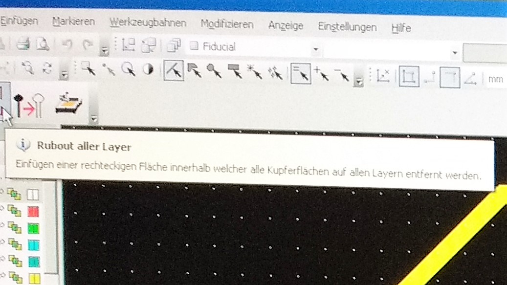
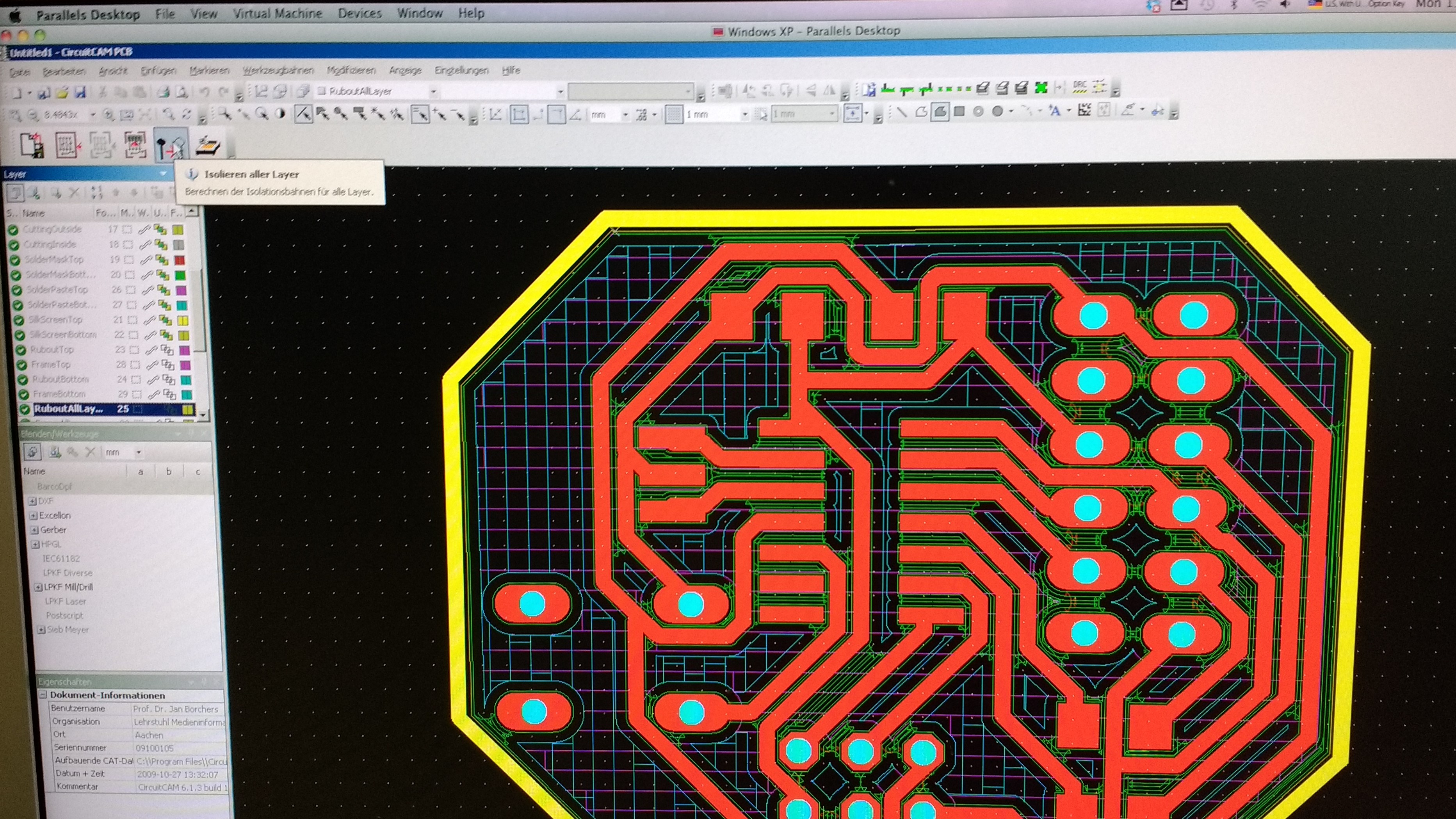
PCB making
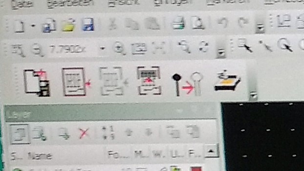
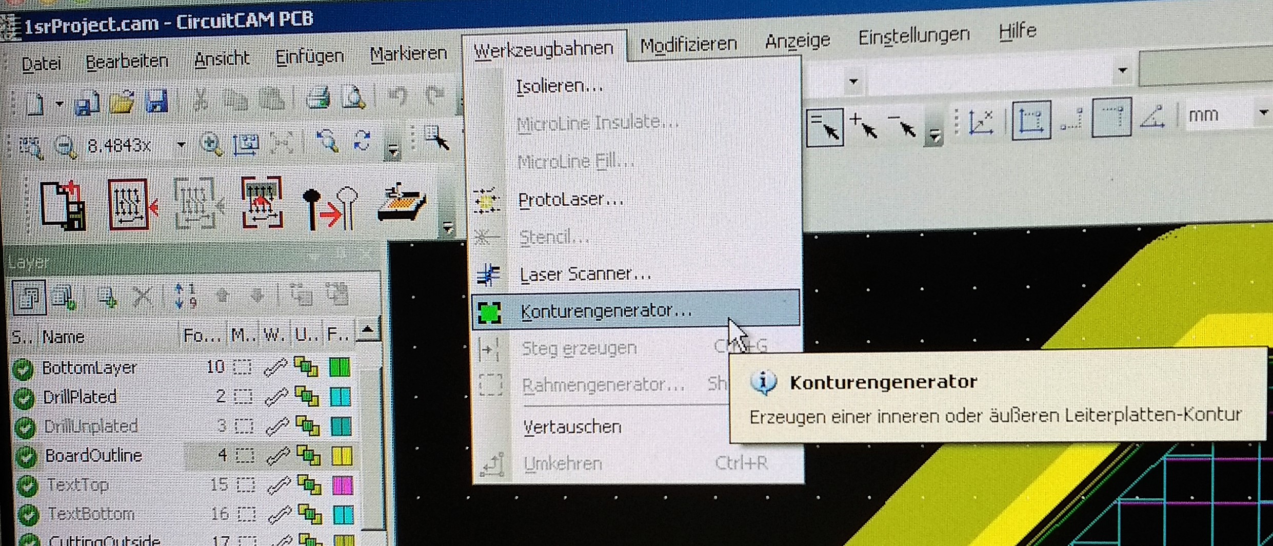
This part is somehow a repetition of week4.Electronics Production, for more detailed information, please refer to a linked page.
I milled single-sided PCB using CircuitCAM and BoardMaster program
along with LPKF Protomat S62 PCB mill in our lab.
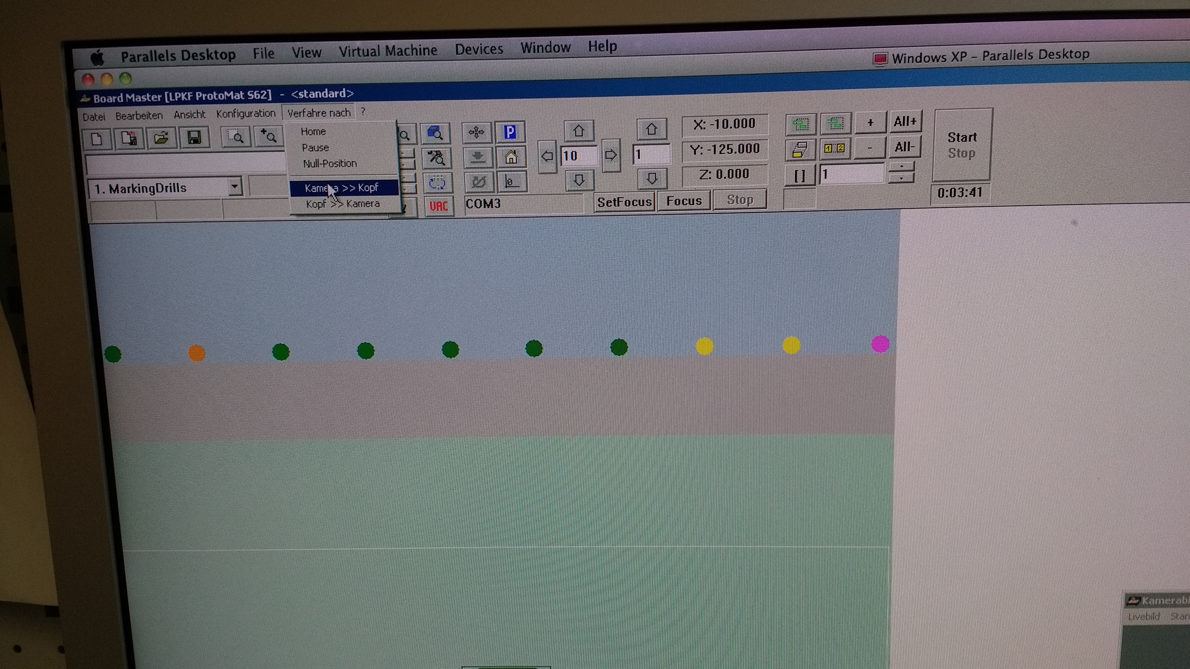
HOW TO: Milling and Soldering
- Create .job file from Gerber files.
- Milling
- Turn Milling machine and vacuum cleaner on.
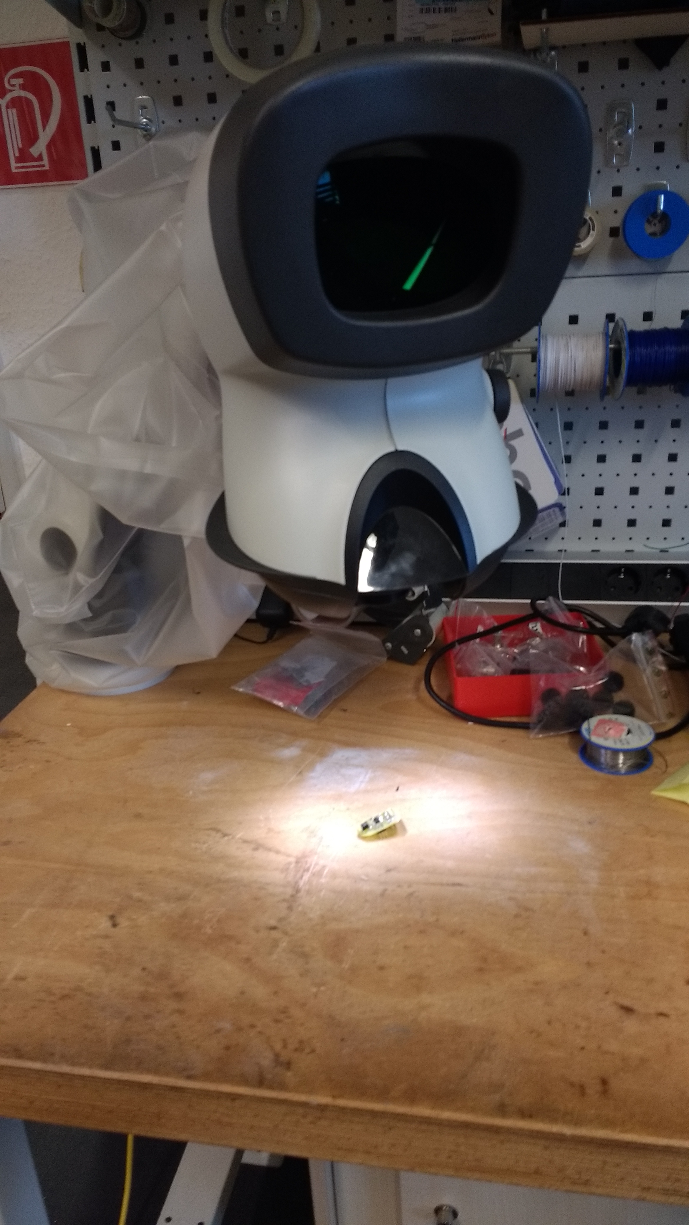
- Move camera to head.
- find the area to cut with camera.
- move a pcb to a cutting orgin point.(Check whether it is set for the all layers, sometimes, layers are placed in different positions).
- Move head to a camera.
- Visit menus in order(1,2,7,10) and operate them(All+, Start).
- When finished move milling device back to home and turn off the software and machine.
- Using Pincett. pick up the milled PCB board from the plate and trim the edge with a sandpaper.
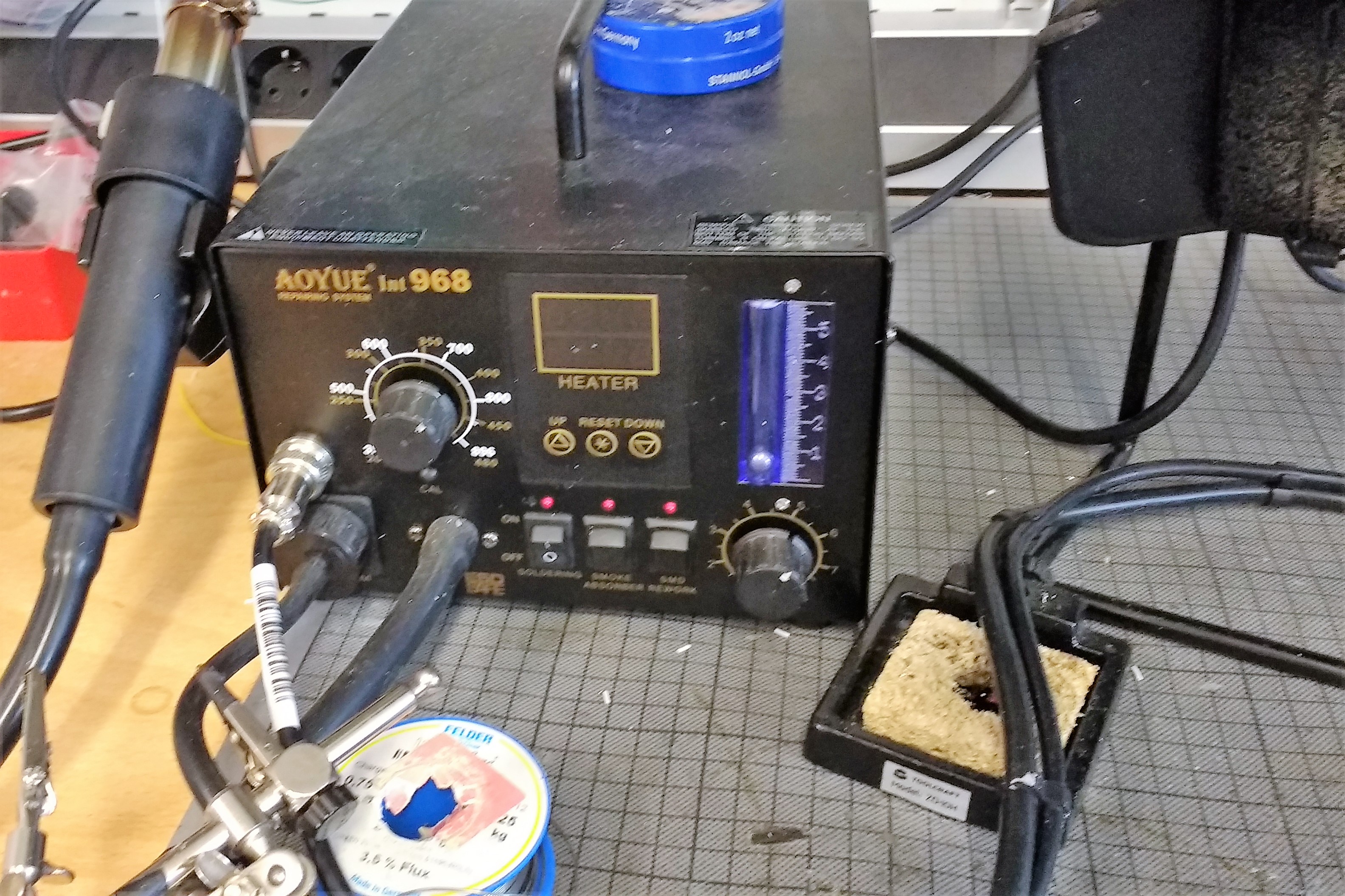
- Soldering
- Prepare right components to solder in PCB.
- Check the direction if required(in my case, switch was the one which require right direction but as the different length of each sides were naturally give an idea of what is the right connection).
- Sit on a soldering station.
- Solder components on PCB.

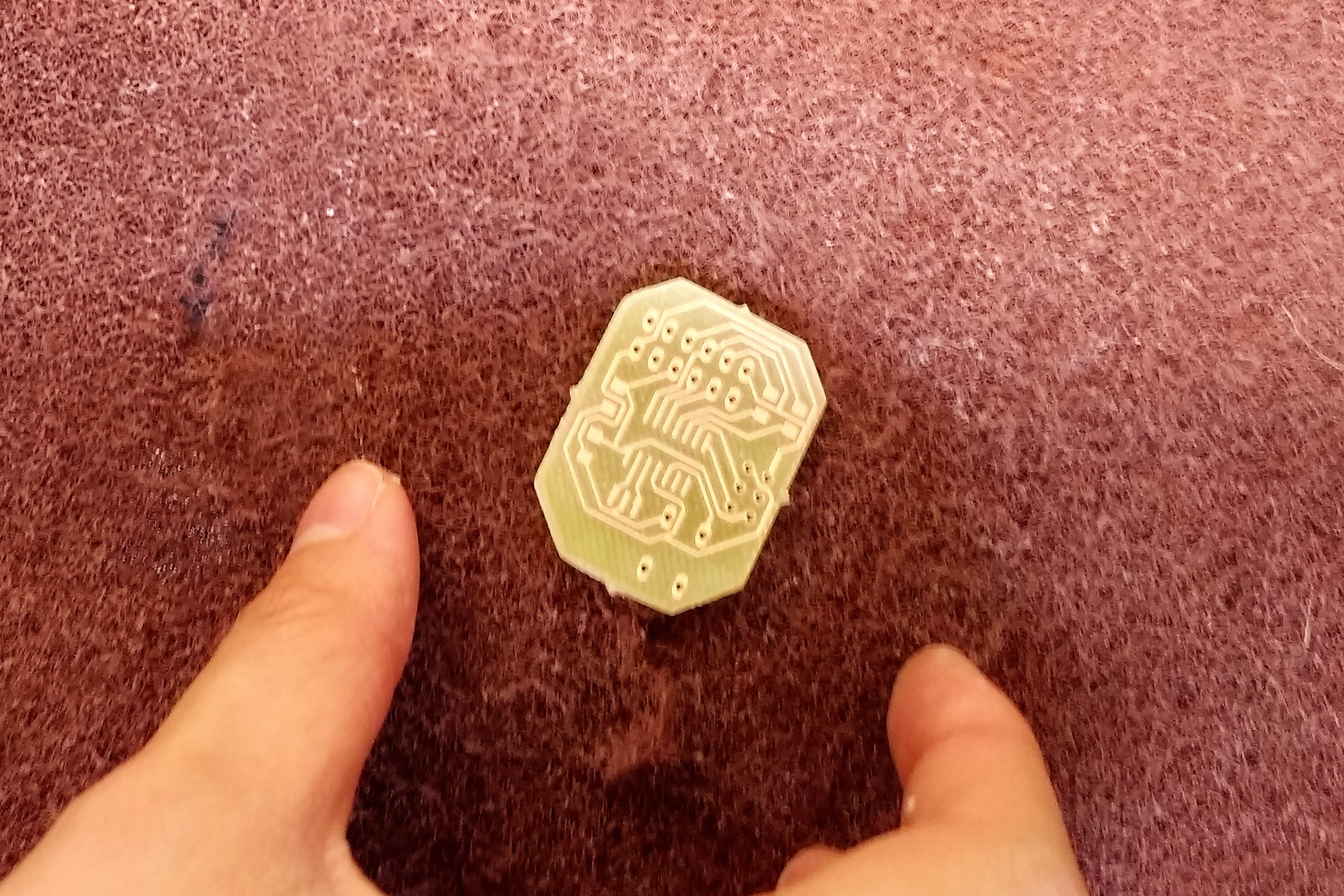
Below are results from the assignment.