Evolution
In this section some info about evolution
Week #2 as my main project is a little in stand-by because of lack of information I have time to work on this project. So if you will look on week#2 assignment you will
found many information about progress I did. So now I have design for the top part of my Soil Sensor. I have ordered some cheap arduino ready sensors so I can start some tests at home with some kitchen flowers of my wife :-). Hope
I will not kill them :-).
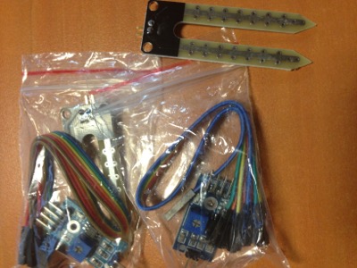
Unboxing cheap soil sensors. Ready to progress.
Real progress
After passing the week of Input devices and week Network and communication I saw how it works "step response loading"
and I2C communication - now let apply it to my boards.
Definition
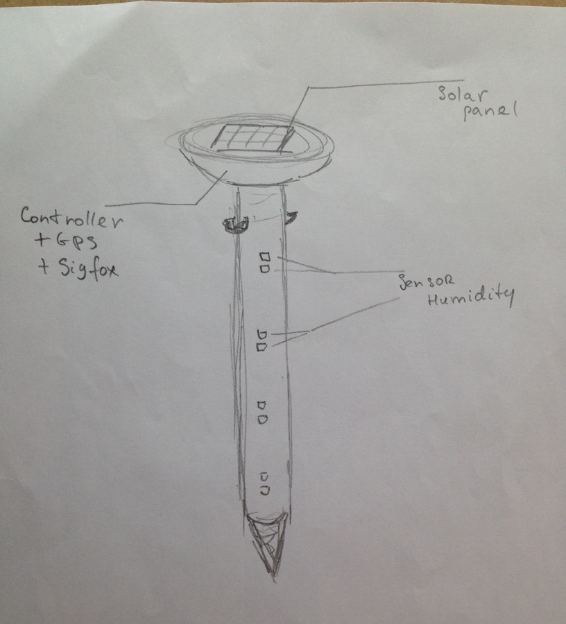
Soil moisture sensor is a small board that has 2 I2C connectors (in / out - just to simplify wiring and join them in serie) and has a sesor connected via 1MOhm resistors that work as step response loading. In network we have N node sensors (they are slave
in I2C network and reply on request from master. And dring the time each node just collect the moisture status of soil by converting analog data received via step response). Also network contain 1 master node (that call each slave
times to time) and some device (either the ESP8266 that send via WiFi data to Node-Red server, either the LCD screen that do outout - see Output devices where I
did exactly for this extra project the output screen)
Design
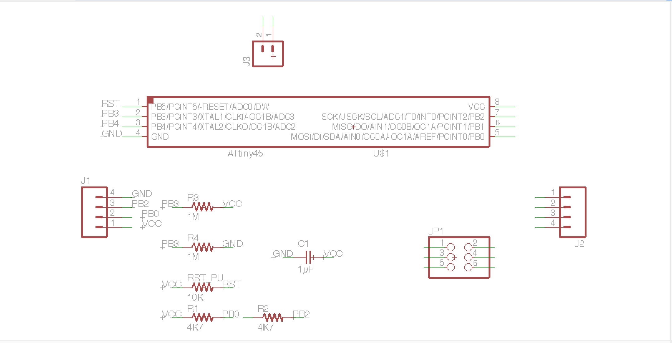
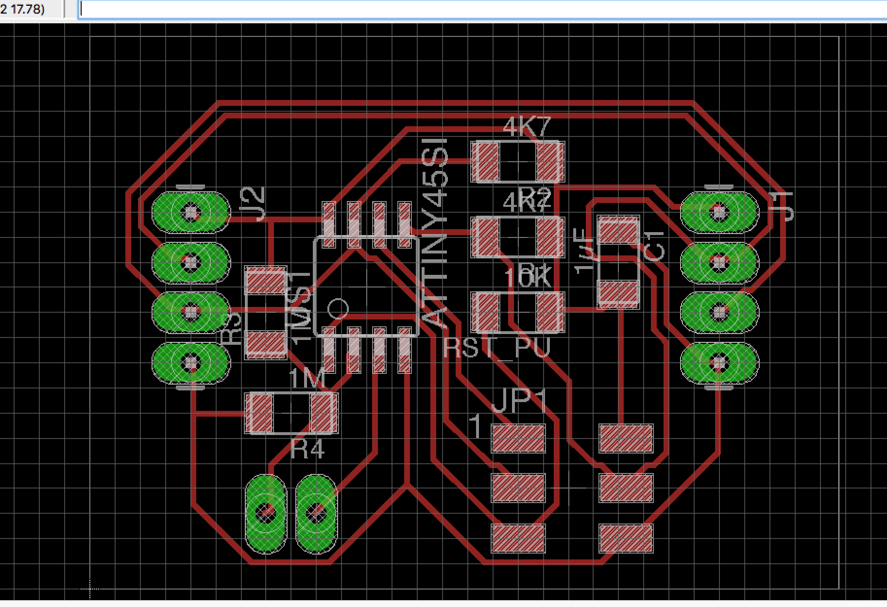
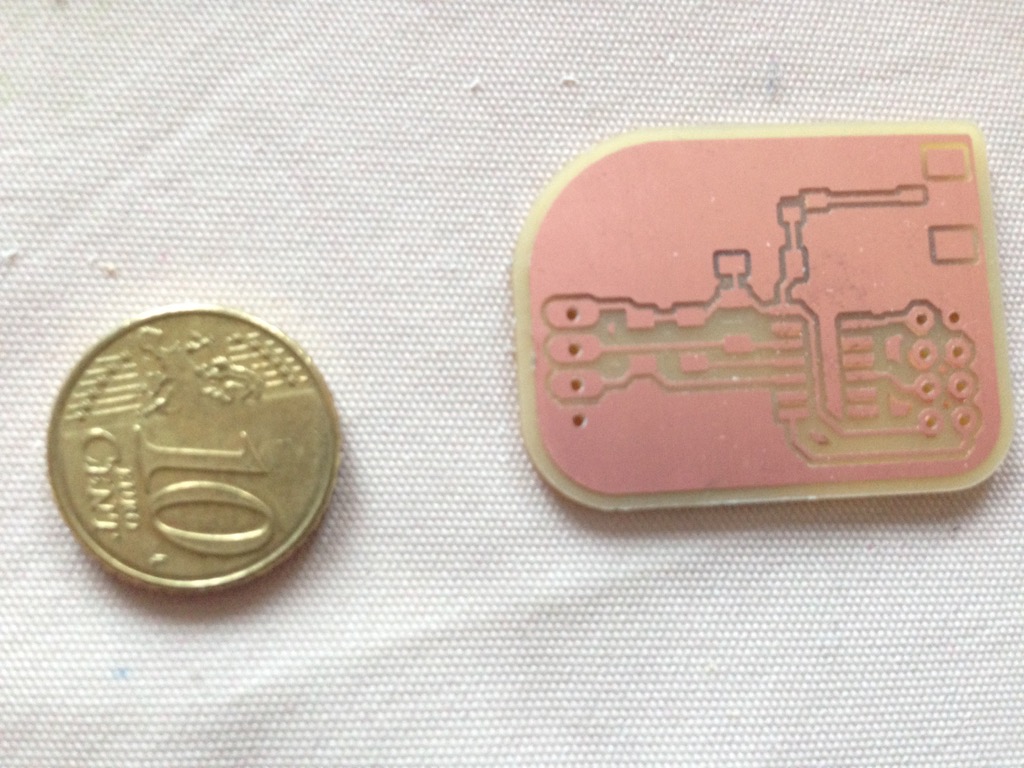
So I started to make nodes in Eagle. My first version of node looks like this:
To speed-up milling - I did it by 6
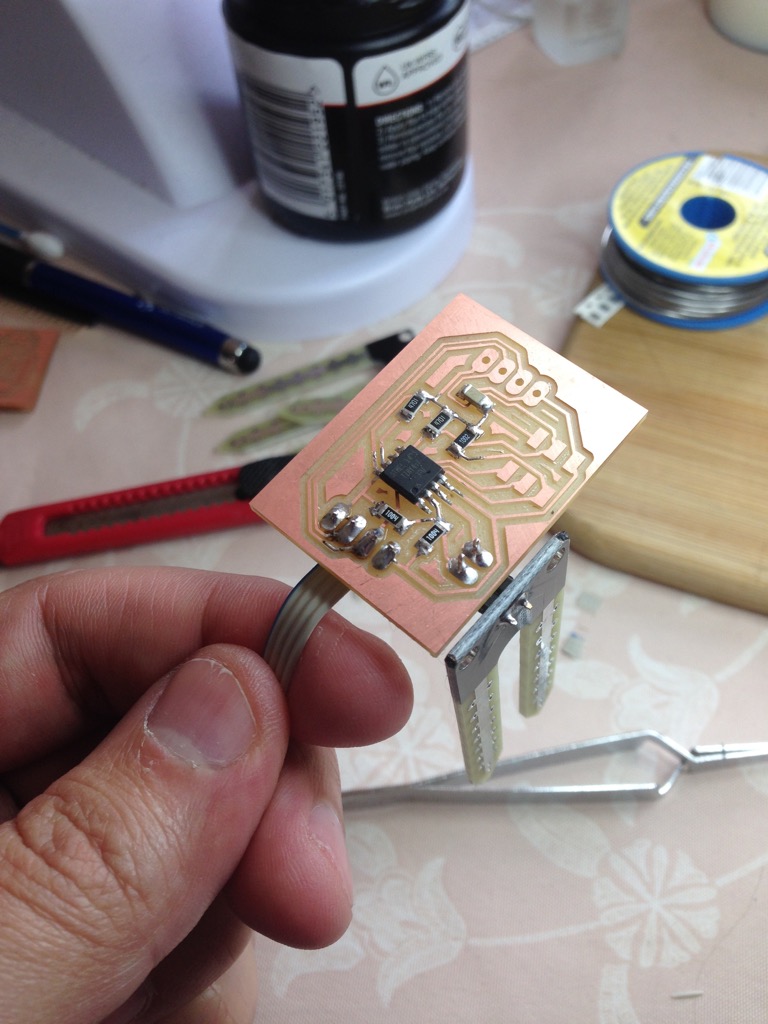
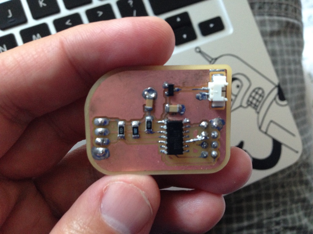
Milling and soldering
When I solder them - I started to learn about how it works I2C communication and I found that I don't need to have on each node the pull-up resistance. So I soldered them just on master node and on the last in line. The first node also have a header pins
to connect to master (just to have a disconnectable wire in one place)
This version works! I tested it and shown results during the Network and communication week assignment.
Let do V2
Few things that I want to improve.
- ISP header
- I don't need the 6 pin header of ISP programmer. I will use my test pince that I have ordered (it makes part of Fabacademy inventory). Using this I can programm my chips directly. So remove header
- Size
- Will reduce size.
- Master node
- Yes, master node need to be designed. I used standard board I2C from the week of networ and communication
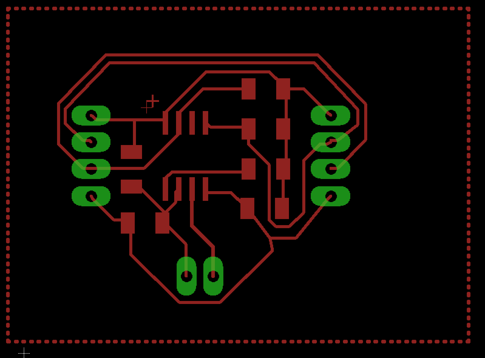
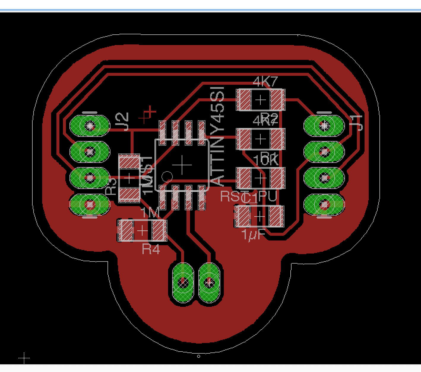
V2 node
So v2 node designed. All changes applied. Below is board (schematic does not have a lot of changes). As well remarked (+) to simplify soldering of avr.
V3 node
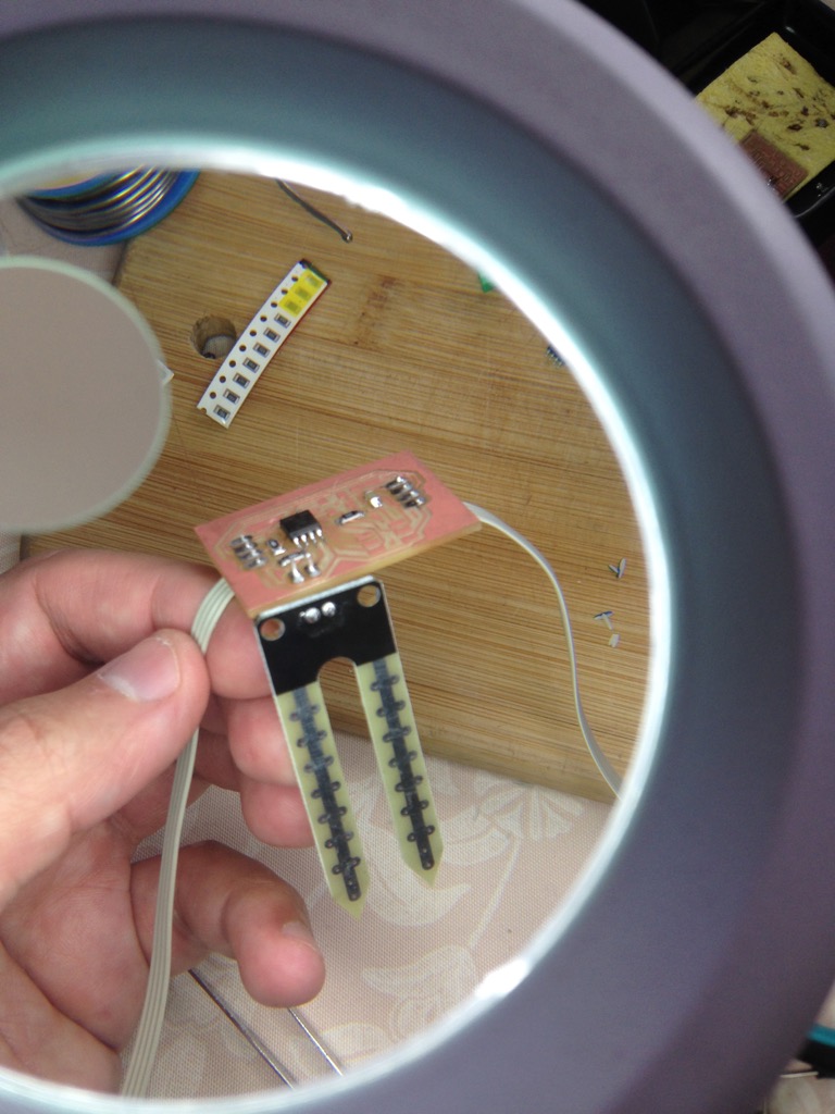
Yes! Directly to v3! :-). V3 has more cool design and I like it much more. Below is one board and pack of 4! :-)
And yes - I milled them (but not yet soldered). Here how it looks like:
Here is the difference between v1 and v3
I found them awesome :-)
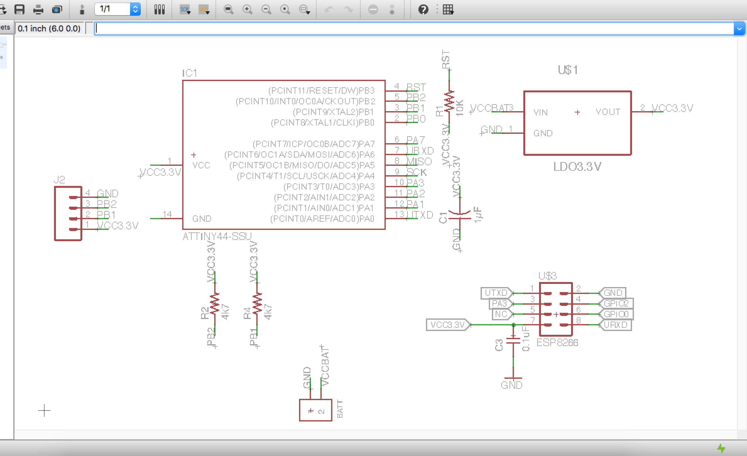
V3 master node
So v3 master node based on Attiny44 (to manage serial and i2c communication, but in reality I find that 45 was enough...) has two different things (important things) - it contain 6 holes that ready to receive esp866 WiFi board. And master node able to
communicate with this WiFi shield by Serial protocol - so it can report own and all slave nodes status directly to server via Internet. IoT! :)
As well master node has 2 type of power - from outside (during programming for example) or from the LiPo battery! (750Mah it should works for weeks without a problem). So below is the design.
Milling master
So milled master and I did v2 before (one trace was not on good place - so updated by wire). In v3 this error fixed. So below is soldered version v2 (worked version)
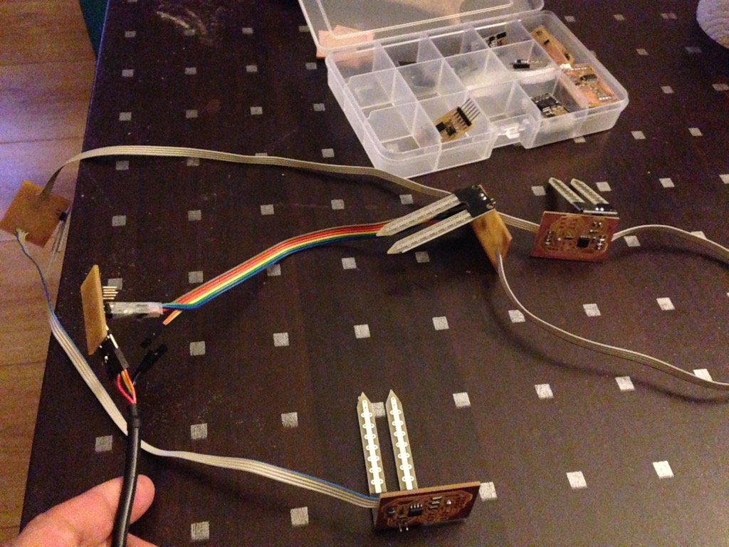
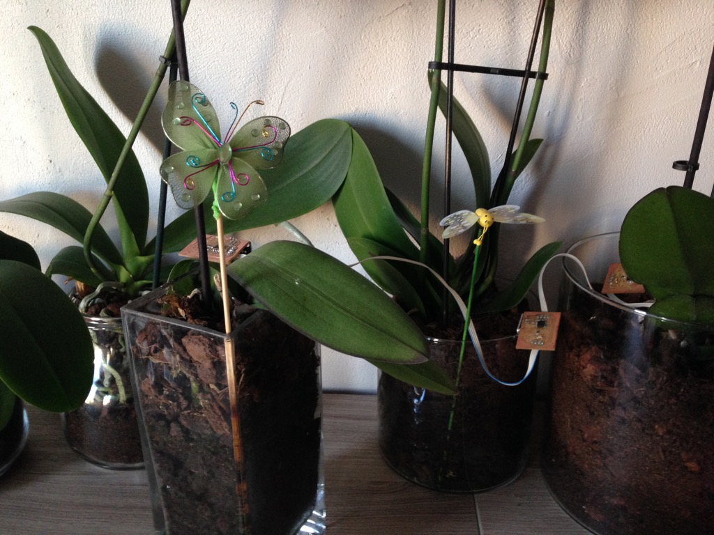
How it looks like
Network is build and tested. So it can be tested in real
Network is build and tested. So it can be tested in real
Will create box for each of them. But next time