Week 8 - Embedded Programming
Assignment
- read a microcontroller data sheet
- program your board to do something, with as many different programming languages and programming environments as possible
Index
Program the board
Arduino Blink Sketch
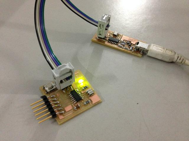
First step was to check if the hello board from week 6 was working fine.
I used a colleague’s FabISP for this, since it was tried and tested.
I downloaded Arduino IDE, and followed the instructions here to setup David Mellis’ Board Manager for the ATtiny.
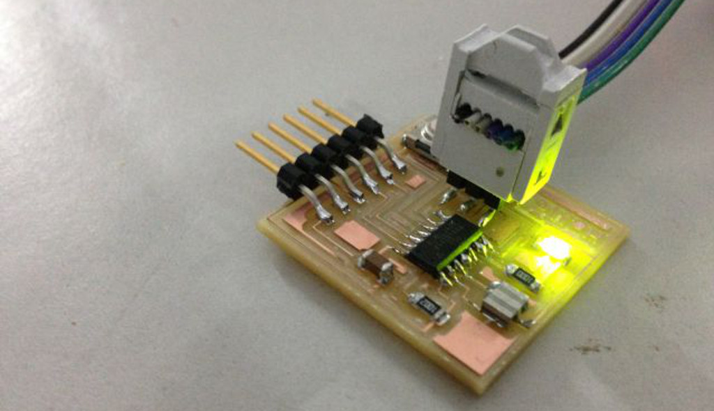
I had connected the LED to PA7 which was on pin 6. I opened up the Examples -> Blink sketch and changed the pin number for the LED from 13 to 6.
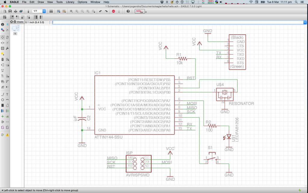
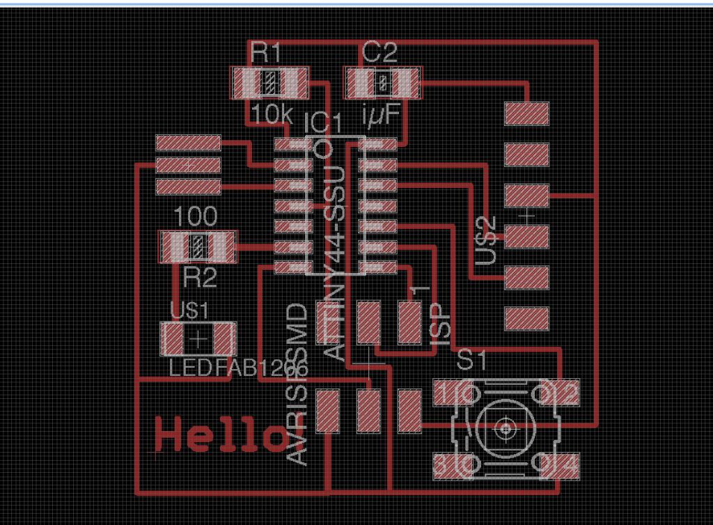
For reference, here are the schematics and layout for the board from week 6 to figure out which pin the LED is connected to:
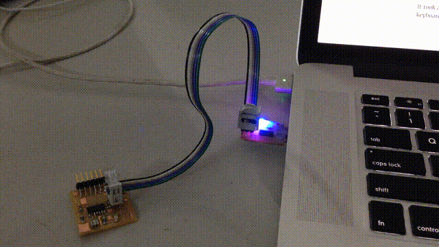
When I uploaded the sketch, the LED on the FabISP started blinking instead of the one on the hello board, so clearly the LED wasn’t on pin 6 but on pin 7:
I then changed the pin number to 7 to match “PA7”:
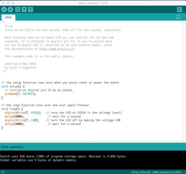
And it worked just fine.
Note the size of the binary in the above image shows 836 bytes. Will compare that to a C and assembly program later.
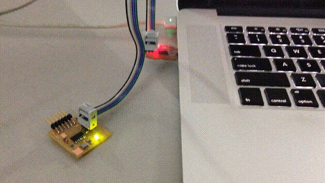
Next I tested it with my FabISP, and that worked fine too! :-)
Here it is:
Original Files
- blink sketch: blink.ino
Arduino Button Sketch
Next I tried the Button sketch. After programming, it was behaving unusually. The LED would turn on and off if I brought my finger close to the LED.
Francisco mentioned that this was because I hadn’t enabled the pull-up resistor and the wire was “floating”.
Arduino docs mention that pinMode should be set to INPUT_PULLUP instead of INPUT to enable the internal pull-up resistor. After changing this it worked correctly - with the LED being on by default because the signal was pulled-up to logical 1 and the code (below) uses this to switch on the LED.
Here is the button sketch with my minor changes:
const int buttonPin = 3;
const int ledPin =  7;

// variables will change:
int buttonState = 0;

void setup() {
  // initialize the LED pin as an output:
  pinMode(ledPin, OUTPUT);
  // initialize the pushbutton pin as an input:
  pinMode(buttonPin, INPUT_PULLUP); // <----- changed from INPUT
}

void loop() {
  // read the state of the pushbutton value:
  buttonState = digitalRead(buttonPin);

  // check if the pushbutton is pressed.
  // if it is, the buttonState is HIGH:
  if (buttonState == HIGH) {
    // turn LED on:
    digitalWrite(ledPin, HIGH);
  } else {
    // turn LED off:
    digitalWrite(ledPin, LOW);
  }
}
Original Files
- button sketch: button.ino
C Blink Program
Next step is to write the LED blink program in C.
I have started reading Make: AVR Programming by Elliot Williams, and I really like this book compared to the couple of others on AVR programming I’ve tried to read.
I used the Makefile generated from avr-project, which is a Crosspack AVR tool available on the Mac.
Next I tried the following code to blink the LED in C.
#include <avr/io.h>
#include <util/delay.h>

#define LED_PIN PA7
const int delay = 1000;

int main(void) {
    DDRA |= (1 << LED_PIN); // sets the data direction of pin 7 in port A to output

    while(1) {
        PORTA |= (1 << LED_PIN);  // writes a high value to pin 7
        _delay_ms(delay);

        PORTA &= ~(1 << LED_PIN); // write a low value to pin 7
        _delay_ms(delay);
    }

    return 0;
}
The output was:
$ make flash
avr-gcc -Wall -Os -DF_CPU=20000000 -mmcu=attiny44 -c blink.c -o blink.o
avr-gcc -Wall -Os -DF_CPU=20000000 -mmcu=attiny44 -o blink.elf blink.o
rm -f blink.hex
avr-objcopy -j .text -j .data -O ihex blink.elf blink.hex
avr-size --format=avr --mcu=attiny44 blink.elf
AVR Memory Usage
----------------
Device: attiny44

Program:     100 bytes (2.4% Full)
(.text + .data + .bootloader)

Data:          0 bytes (0.0% Full)
(.data + .bss + .noinit)


avrdude -c usbtiny  -p attiny44 -U flash:w:blink.hex:i

avrdude: AVR device initialized and ready to accept instructions

Reading | ################################################## | 100% 0.00s

avrdude: Device signature = 0x1e9207
avrdude: NOTE: "flash" memory has been specified, an erase cycle will be performed
         To disable this feature, specify the -D option.
avrdude: erasing chip
avrdude: reading input file "blink.hex"
avrdude: writing flash (100 bytes):

Writing | ################################################## | 100% 0.13s

avrdude: 100 bytes of flash written
avrdude: verifying flash memory against blink.hex:
avrdude: load data flash data from input file blink.hex:
avrdude: input file blink.hex contains 100 bytes
avrdude: reading on-chip flash data:

Reading | ################################################## | 100% 0.15s

avrdude: verifying ...
avrdude: 100 bytes of flash verified

avrdude: safemode: Fuses OK (H:FF, E:DF, L:62)

avrdude done.  Thank you.
It shows that the program size is 100 bytes, which is much smaller than the one generated through the Arduino Sketch (836 bytes).
The LED did start blinking, but it isn’t blinking as fast as it should - the delay seems more like 2 sec than 100ms.
The makefile had a variable defined called CLOCK, which was set to 20000000. I changed it to 1000000 (got this hint from the Arduino status bar which reported “ATtiny44, 1Mhz internal”). With this change it started working correctly.
The datasheet says this in Section 6.2.6 (page 30) about the “Default Clock Source”:
The default clock source setting is therefore the Internal Oscillator running at 8.0 MHz with longest start-up time and an initial system clock prescaling of 8, resulting in 1.0 MHz system clock.
Original Files
Assembly Blink program
Next step is to program in assembly language.
I’m going through tutorials on AVR Beginners for this.
Toolchain setup
I’ve installed avra assembler using homebrew, since gavrasm is available only for Windows and Linux.
I used Francisco’s code to check if avra was working as expected.
I had to add the following line to include the declarations file for the attiny44 from here.
.include tn44def.inc
I ran:
avra blink.asm
and it output:
$ make flash
avrdude -c usbtiny -p attiny44 -U flash:w:blink.hex:i

avrdude: AVR device initialized and ready to accept instructions

Reading | ################################################## | 100% 0.00s

avrdude: Device signature = 0x1e9207
avrdude: NOTE: "flash" memory has been specified, an erase cycle will be performed
         To disable this feature, specify the -D option.
avrdude: erasing chip
avrdude: reading input file "blink.hex"
avrdude: writing flash (8 bytes):

Writing | ################################################## | 100% 0.05s

avrdude: 8 bytes of flash written
avrdude: verifying flash memory against blink.hex:
avrdude: load data flash data from input file blink.hex:
avrdude: input file blink.hex contains 8 bytes
avrdude: reading on-chip flash data:

Reading | ################################################## | 100% 0.07s

avrdude: verifying ...
avrdude: 8 bytes of flash verified

avrdude: safemode: Fuses OK (H:FF, E:DF, L:62)

avrdude done.  Thank you.
This worked, but the LED appeared to be on continuously since there was no delay in the code.
Next step is to add in some delay. This could be done by using interrupts or by keeping the processor busy for the expected time-period.
The following code uses 2 registers as a single 16 bit value and increments it till there is an overflow. This introduces a small delay which makes the LED blinking visible.
clr r24                 ; clear register to use as part of word
clr r25                 ; clear register to use as part of word
delay_loop1:
adiw r24, 1             ; add 1 to the word starting at r24
brne delay_loop1        ; loop until overflow
The total time taken is calculated as follows (refer to the AVR Instruction Set Manual for the clock-cycles for a specific instruction. The ATtiny datasheet also provides this information at the end:
- clr: 1 cycle
- adiw: 2 cycles
- brne: 2 cycles when no overflow, 1 on overflow
Delay cycles =
    2 * clr(1 cycle)
    + 65536 * looping(4 cycles)
    + 1 * overflow(3 cycles)
    = 2 + 262144 + 3
    = 262149
Given that the clock is running prescaled at 1mhz == 1µs per clock cycle, the delay is 262149µs or ~ 262ms.
Here is the full code with delays:
; blink.asm
;
; Blink LED

.include "tn44def.inc"

.org 0              ; sets the programs origin

sbi DDRA, 7         ; set bit in Data Direction Register to mark the pin as output

loop:
sbi PORTA, 7        ; turn on the LED

clr r24             ; clear register to use as part of word
clr r25             ; clear register to use as part of word
delay_loop1:
adiw r24, 1         ; add 1 to the word starting at r24
brne delay_loop1    ; loop until overflow

cbi PORTA, 7        ; turn off the LED

clr r24             ; clear register to use as part of word
clr r25             ; clear register to use as part of word
delay_loop2:
adiw r24, 1         ; add 1 to the word starting at r24
brne delay_loop2    ; loop until overflow

rjmp loop
Original Files
- Blink asm program: blink.asm
- Makefile: Makefile
- Directives file: tn44def.inc
Program Size Comparisons
The output of avrdude shows the program size for the blink LED programs:
-
Arduino sketch: 836 bytes
-
C program: 100 bytes
-
Assembly program: 8 bytes
$ avr-objdump -j .sec1 -d -m avr blink.hex

blink.hex:     file format ihex


Disassembly of section .sec1:

00000000 <.sec1>:
   0:	d7 9a       	sbi	0x1a, 7	; 26
   2:	df 9a       	sbi	0x1b, 7	; 27
   4:	88 27       	eor	r24, r24
   6:	99 27       	eor	r25, r25
   8:	01 96       	adiw	r24, 0x01	; 1
   a:	f1 f7       	brne	.-4      	;  0x8
   c:	df 98       	cbi	0x1b, 7	; 27
   e:	88 27       	eor	r24, r24
  10:	99 27       	eor	r25, r25
  12:	01 96       	adiw	r24, 0x01	; 1
  14:	f1 f7       	brne	.-4      	;  0x12
  16:	f5 cf       	rjmp	.-22     	;  0x2
It was interesting that the clr instruction was replaced by an eor (Exclusive OR) of the register with itself.
The size seems more than 8 bytes. Also avr-size shows the size as 24 bytes… not sure why avrdude mentions “8 bytes of flash verified”.
$ avr-size blink.hex
   text	   data	    bss	    dec	    hex	filename
      0	     24	      0	     24	     18	blink.hex
Interrupt-based program
Here is a program, which continuously blinks the LED every 100ms. On pressing the button (and holding it down), the LED is turned off for 1 sec before resuming blinking. On releasing the button, the LED is turned on for 1 sec before resuming blinking.
This is implemented using interrupts, see the commented code below.
Notes:
- The INT0 interrupt allows triggering changes on pin low, pin change, pin high edge, pin low edge.
- INT0 on the attiny44 is available on pin PB2.
- It supports 2 pin change interrupts PCINT0 and PCINT1.
- PCINT0 handles pin changes on pins 0:7, PCINT1 handles pins 8:11
- Bits in PCMSK0 and PCMSK1 need to be set to indicate which specific pin the program is interested in.
#include <avr/io.h>
#include <avr/interrupt.h>
#include <util/delay.h>

#define LED_DDR     DDRA
#define LED         PA7
#define LED_PORT    PORTA

#define BUTTON_PORT PORTA
#define BUTTON      PA3
#define BUTTON_PIN  PINA

const int delay = 100;

ISR(PCINT0_vect) {
    // by default the bit will have a high value because of the pull-up resistor
    if(bit_is_set(BUTTON_PIN, BUTTON)) {    // this is true when a pressed button is released
        LED_PORT |= (1 << LED);             // turn LED on
        _delay_ms(1000);                    // so we can see the change
    } else {                                // this will happen when the button is pressed
        LED_PORT &= ~(1 << LED);            // turn LED off
        _delay_ms(1000);
    }
}

void initPinChangeInterrupt(void) {
    GIMSK |= (1 << PCIE0);              // enable pin change interrupt 0
    PCMSK0 |= (1 << BUTTON);            // ... only for the button
    sei();                              // enable interrupts globally
}

int main(void) {
    LED_DDR |= (1 << LED);              // mark LED as output
    BUTTON_PORT |= (1 << BUTTON);       // mark button as input and enable pull-up resistor

    initPinChangeInterrupt();

    while(1) {
        _delay_ms(delay);
        LED_PORT ^= (1 << LED);         // toggle the LED
    }
    return 0;
}
Original Files
- C source: button-int.c
- Makefile: Makefile
Timer Blink
This program implements the blink logic as a timer event rather than a delay loop. Here is the commented code:
#include <avr/io.h>
#include <avr/interrupt.h>
#include <util/delay.h>

#define LED_DDR     DDRA
#define LED         PA7
#define LED_PORT    PORTA

ISR(TIM0_OVF_vect) {
  // interrupt occurs every:
  //    1000000 / 1024 * 256
  //    = ~ 250000 clocks
  //    = ~250 ms (since clock is 1mhz and 1 clock cycle = 1µs)
  // Note: 1024 is the clock prescaler
  //        256 is the overflow limit for the 8 bit counter

  LED_PORT ^= (1 << LED);   //toggle led pin
}

void initTimerInterrupt(void) {
  TCCR0B |= (1<<CS02) | (1<<CS00);          //clock select: prescale timer clk/1024
  TIMSK0 |= (1<<TOIE0);                     //enable timer overflow interrupt
  sei();                                    // globally enable interrupts
}

void main(void) {
    LED_DDR |= (1 << LED);              // mark LED as output
    initTimerInterrupt();
    while(1);                           // loop forever
}
Original Files
Software UART Implementation
For debugging puproses it would be useful to output some data through the serial interface and display it on a host terminal.
However, the ATtiny44 does not have a UART implementation in hardware, instead it supports SPI.
The goal of this mini-project is to implement a software UART interface that allows debugging output to be written out.
Here is a first attempt:
#include <avr/io.h>
#include <avr/interrupt.h>
#include <util/delay.h>

#define CLOCK 1e6
#define BAUD 9600

#define STX_PORT PORTA
#define STX_PIN  0

#define LED_PIN PA7

#define BUTTON_PORT PORTA
#define BUTTON      PA3
#define BUTTON_PIN  PINA

#define MICROSECONDS_PER_BIT (CLOCK / BAUD)

static uint8_t start_sending = 0;


ISR(PCINT0_vect) {
    blinkLED();
    start_sending = 1;
}


void initPinChangeInterrupt(void) {
    GIMSK |= (1 << PCIE0);              // enable pin change interrupt 0
    PCMSK0 |= (1 << BUTTON);            // enable pin change only for button
}


void sendByte(uint8_t c) {
    STX_PORT &= ~(1<<STX_PIN);            // start bit
    _delay_us(MICROSECONDS_PER_BIT);              // bit duration

    uint8_t mask;

    for(mask = 0x01; mask; mask <<= 1) {        // data bits
        if( c & mask ) {
            STX_PORT |= 1<<STX_PIN;           // data bit 1
        } else {
            STX_PORT &= ~(1<<STX_PIN);        // data bit 0
        }
        _delay_us(MICROSECONDS_PER_BIT);
    }

    STX_PORT |= 1<<STX_PIN;           // stop bit
    _delay_us(MICROSECONDS_PER_BIT);
}


void blinkLED() {
    PORTA |= (1 << LED_PIN);  // writes a high value to pin 7
    _delay_ms(100);
    PORTA &= ~(1 << LED_PIN); // write a low value to pin 7
    _delay_ms(100);
}

int main(void) {
    DDRA |= (1 << LED_PIN);
    BUTTON_PORT |= (1 << BUTTON);       // mark button as input and enable pull-up resistor

    initPinChangeInterrupt();
    sei();                              // globally enable interrupts

    uint8_t i = 0;

    for(;;){
        if(start_sending) {
            sendByte(65);  // Send byte of data
            i++;                // Add one to the counter

            if(i == 10){        // End of Data
                i = 0;              // Reset Counter
                _delay_ms(500);      // Delay a bit before sending another block of data
                blinkLED();
            }
        }
    }

    return 0;
}
I used screen and pyserial to connect from my laptop via an FTDI board to the hello board, but it was not able to output the data that was being written.
I did test that the setup was working fine by connecting the RX & TX pins on the FTDI board, and it was successfully echoing whatever I typed into the terminal.
Need to debug this further.
Original Files
ATtiny44 Datasheet Review
This datasheet covers ATtiny24 / 44 / 84. We’re using the ATtiny44.
- Key features
- RISC - mostly single clock cycle execution instructions
- Speed - upto 20mhz at 4.5 - 5.5 V (upto 10mhz at 2.7 - 4.5 V)
- Low power mode
- 32 8bit registers
- 4K ISP flash
- 256b SRAM
- Memory
- Separate data and program memory, also EEPROM for data
- 4k program memory for tiny44 - 2k x 16b locations (1 instructions takes 16 / 32b)
- SRAM first 32b for register file next 64b for IO registers next 256b for data access time is 2 clock cycles: 1 to compute address, 1 to access
- EEPROM 256b
- Fuse bytes
- 3b of non-volatile memory
- bits to control important settings like clock source, debugWire enable, etc
- Status Register
- updated after every instruction
- bit 7 - Global Interrupt Enable bit
- is cleared by hardware when an interrupt occurs, is set by RETI instruction to enable subsequent interrupts
- Register File
- 32 general purpose registers
- Also have an address as the first 32 locations of user data space
- Stack pointer
- separate stacks for subroutines and interrupts
- Instruction execution timing
- Within 1 clock cycle: fetch 2 register operands, execute ALU operation, store result into register
- Reset & Interrupt handling
- interrupt vector stored in program space
- interrupts have priorities - RESET has highest, next is INT0 - External Interrupt Request 0
- takes 4 clock cycles to start executing interrupt routine code, and 4 to return from it
- Clock
- multiple clock sources possible
- external
- internal 8mhz
- default source with prescaling to 1mhz
- internal 128khz
- internal 32khz
- multiplexer selects one based on fuse set
- this is passed through a prescaler, which divides the clock source to reduce power consumption
- this “system” clock feeds into AVR Clock Control Unit, which provides different clock domains - CPU, IO, ADC, Flash
- system clock output can be sent to the CKOUT pin by setting a fuse
- clock timing checks and calibration?
- multiple clock sources possible
- Power Management and Sleep Modes
- 4 sleep modes: idle, ADC noise reduction, power-down, stand by
-
Brown Out Detection disable?
- Reset
- 4 sources:
- Power On Reset:
- External reset: low value on the RESET pin
- BOD reset: triggered when voltage drops below a threshold
- Watchdog timer: triggered when timer fires
- 4 sources:
- Watchdog Timer
- generates a reset pulse when a given delay is exceeded, and a WDR (Watchdog Reset) instruction has not been executed
- IO
- pins can be marked as input or output using DDRxn bit, input is 0, output is 1
- pull-up resistor can be enabled on input pins by setting PORTxn to 1
- 8bit / 16bit Timer/Counter with PWM
- can be used to time program execution, waveform generation
-
Universal Serial Interface?
- Analog Comparator
- Can monitor voltages on AIN0 (postive) and AIN1(negative) and trigger an interrupt or output a value when the positive voltage is higher than the negative one
-
ADC?
- DebugWire
- bi-directional interface to control program flow, execute instructions and program non-volatile memories
- uses RESET port pin
- Self Programming Mechanism for Flash
- allows MCU to download and upload code using any data interface and write to program flash memory
- Bootloader?
Notes
-
Clock signal: edge-triggered, value can be read or written only at clock-edge (rising or falling) clocked flip-flop, latch
-
Multiplexer: data selector, selects 1 signal from many and forwards to its output n selector lines can have 2^n input signals
-
Datapath: 2 types of elements: combinational (ALU), state aka “sequential” logic components (memory, registers) 1 clock signal involves reading from a state element, maybe register, passing it through combinational logic and saving to a state element
-
Registers 1 flip-flop per bit, clock signal, control signal on clock signal, check control and load in parallel from input or hold value
Questions
- “Fully static operation”?