Assignment 04
Electronics Production
Assignment:
Make the Fab (tiny) ISP in-circuit programmer.
Learning outcomes:
- Describe the process of production
- Demonstrate correct workflows and identify areas of improvements, if required
Have you:
- [x] Shown how you made the board
- [x] Explained any problems and how you fixed them
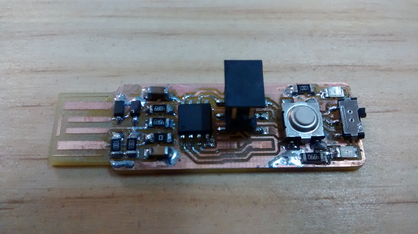
- [x] Included a 'hero shot' of your board
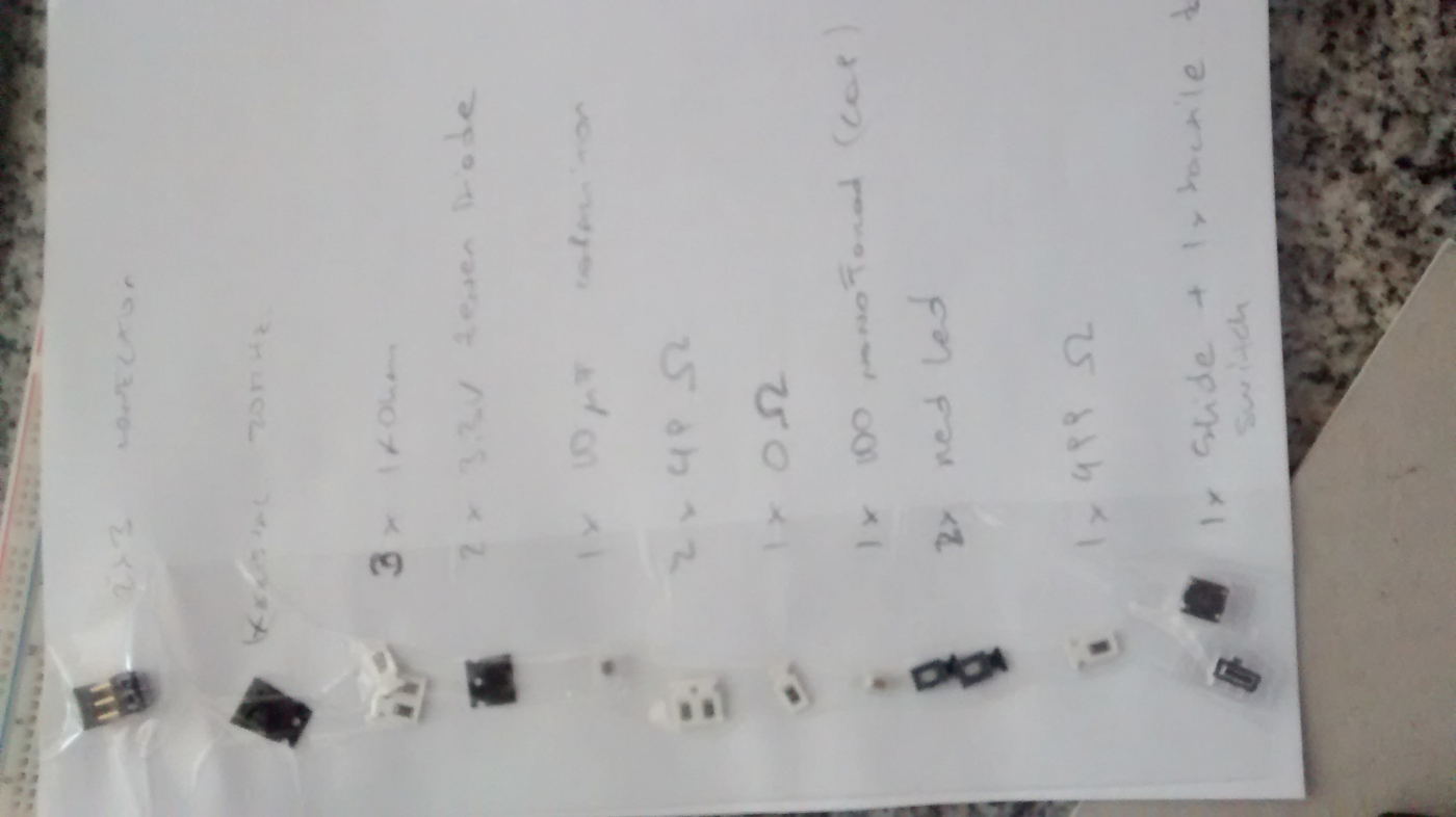
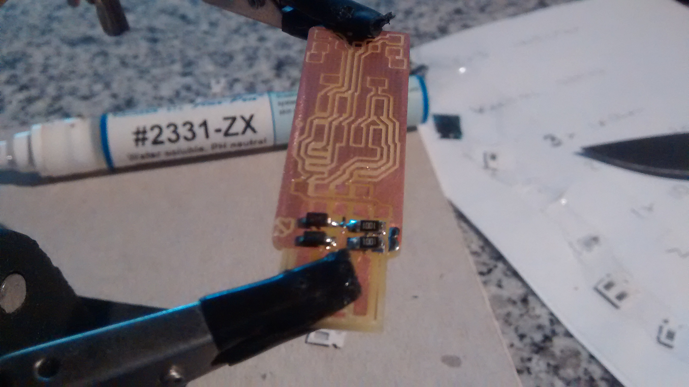
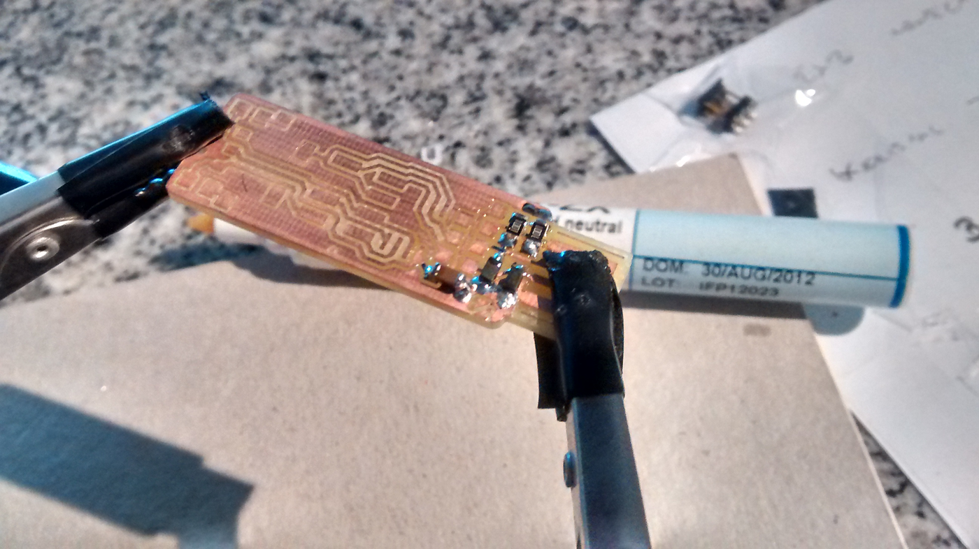
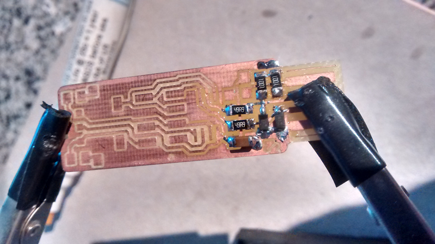
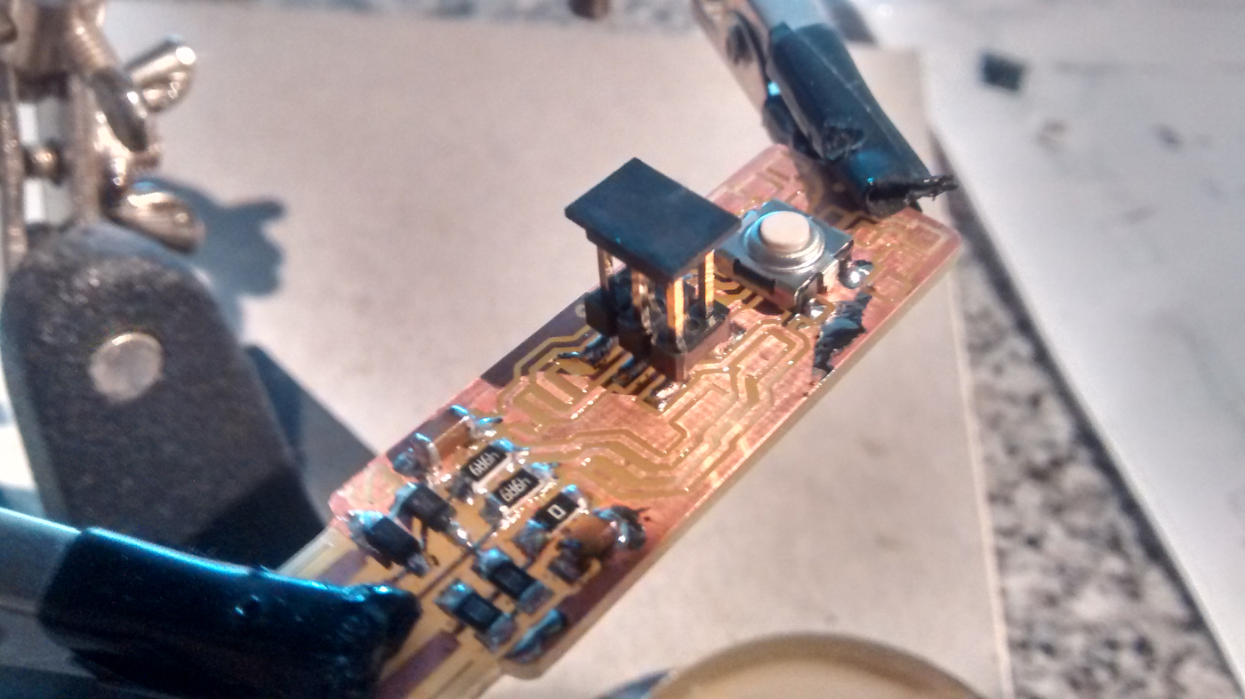
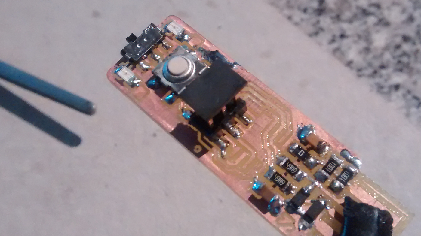
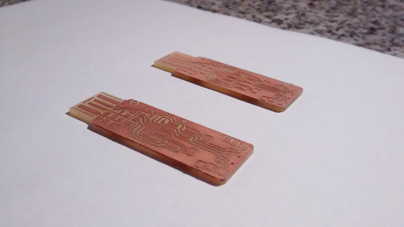
Well, first thing was to arrange all the required tools and parts to start soldering, so I gathered all the SMD component and labeled them (most of them are really tiny and easy to confuse, so I strongly recomend to be neat with the parts). I also used flux on the PCB surface before solder, which helps to remove corrosion during the soldering process.
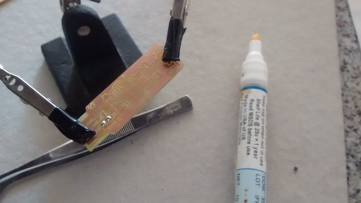
So, as tought, I started the soldering process by placing a single tin drop on the place where the component will be in order to fix it. Soon I realized that it was better to add tin to the soldering iron and to solder only with that amount of tin instead of adding tin continuosly to the PCB-component-iron joint because it is VERY easy that you add too much tin to the joint and that it mess beyond the intended soldering area. In fact, the very first try made to tracks to join which I had to repare by knife cutting the unintended joint.
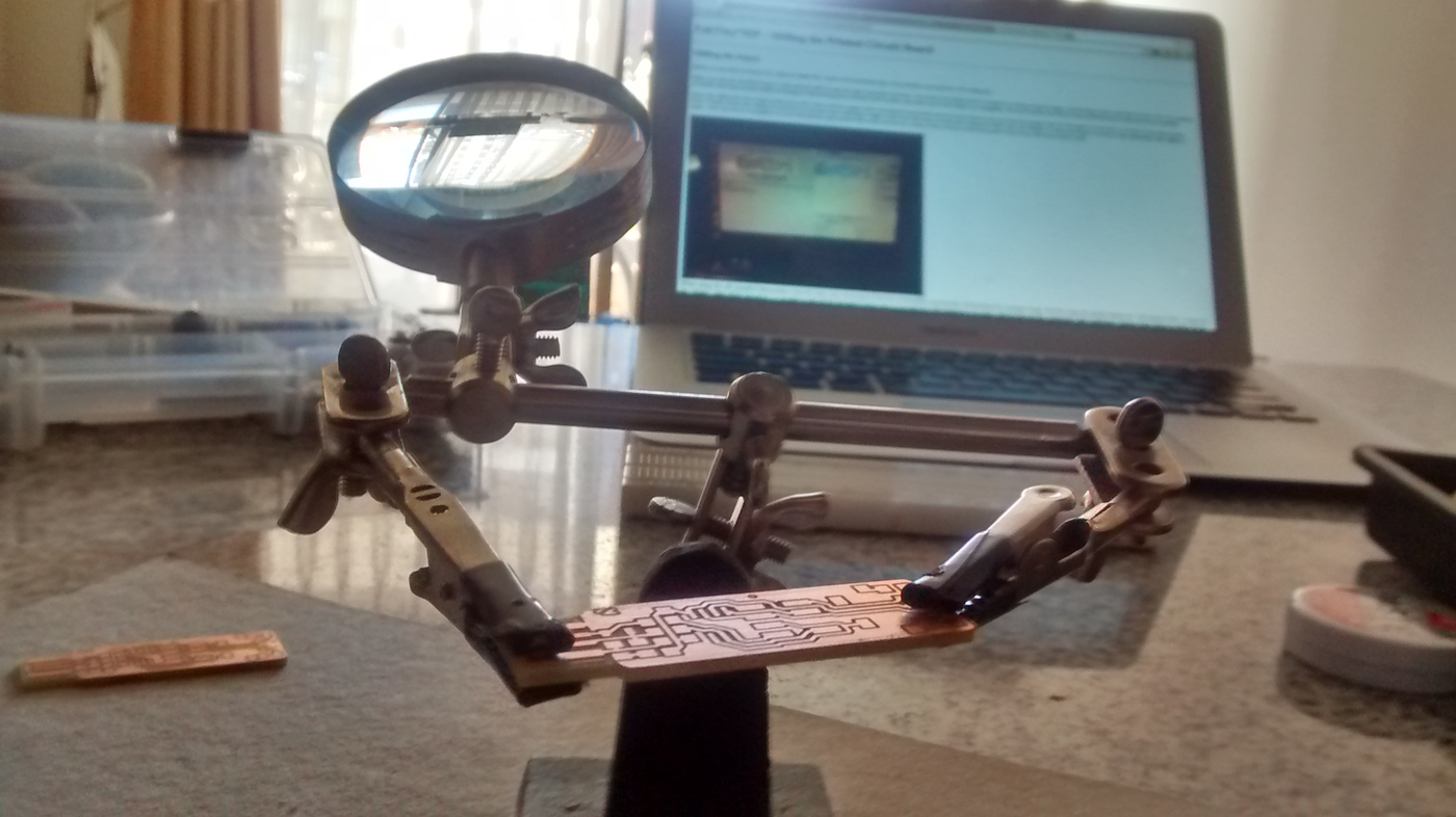
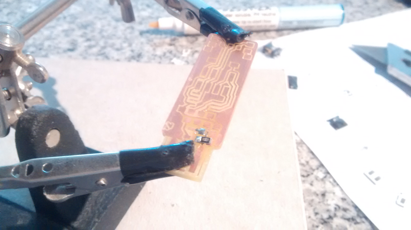
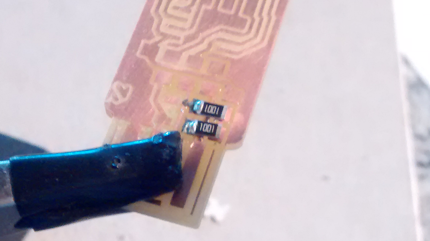
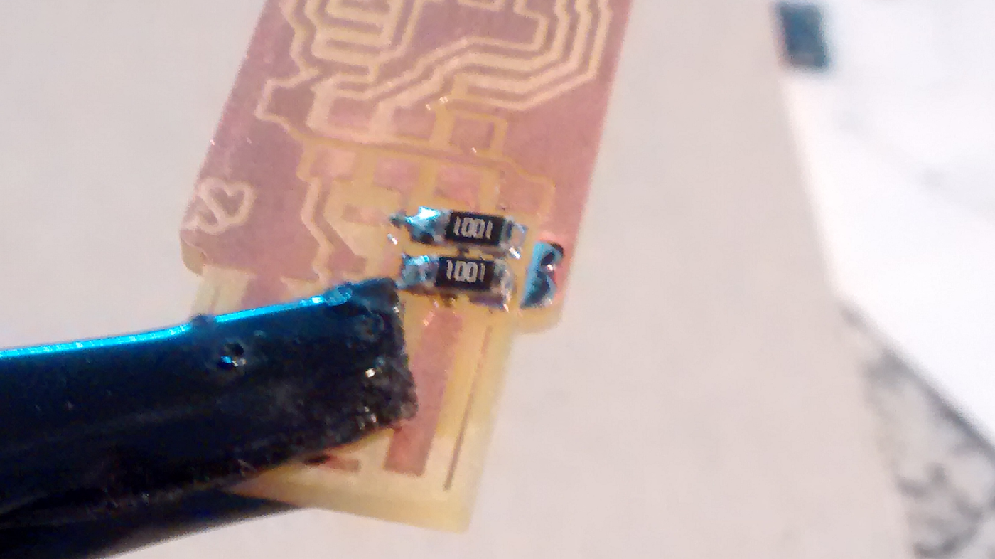
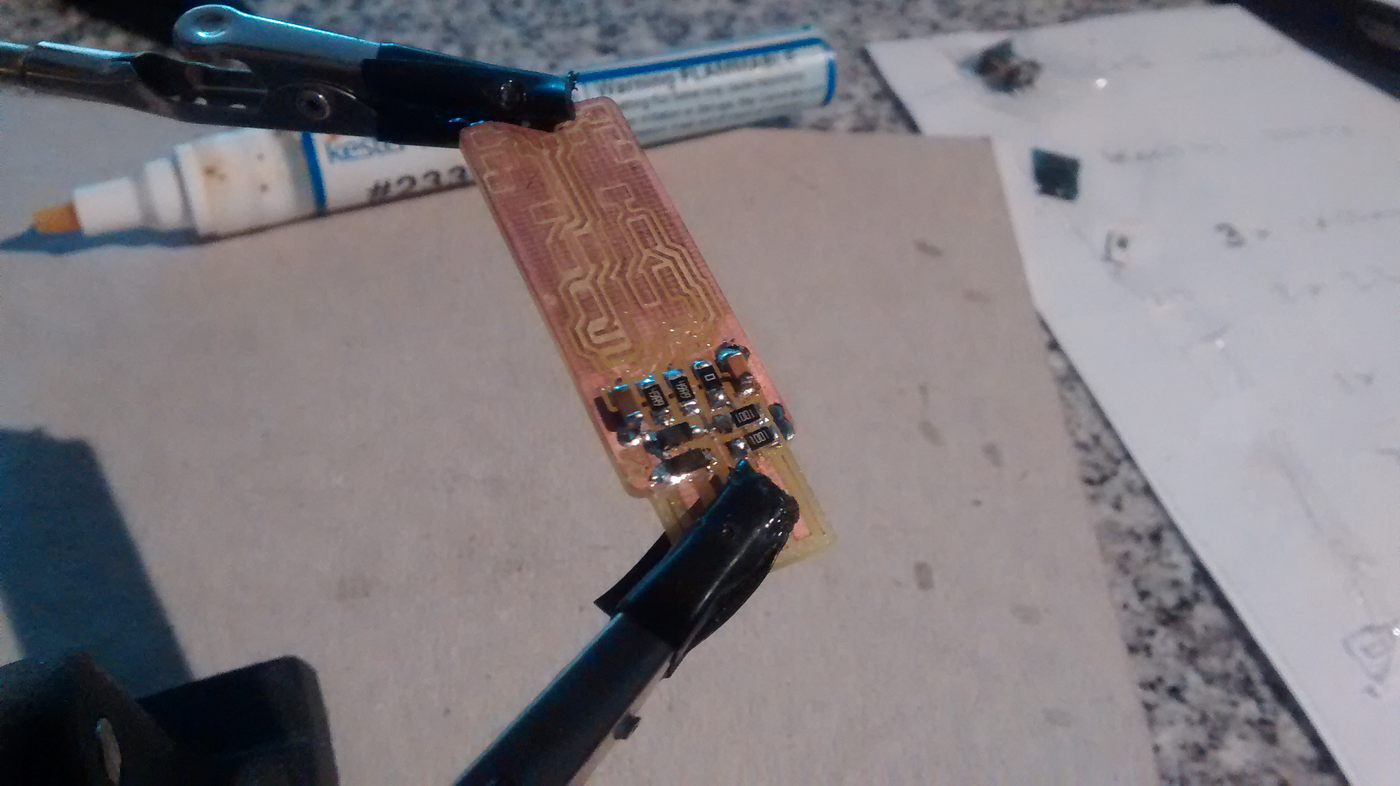
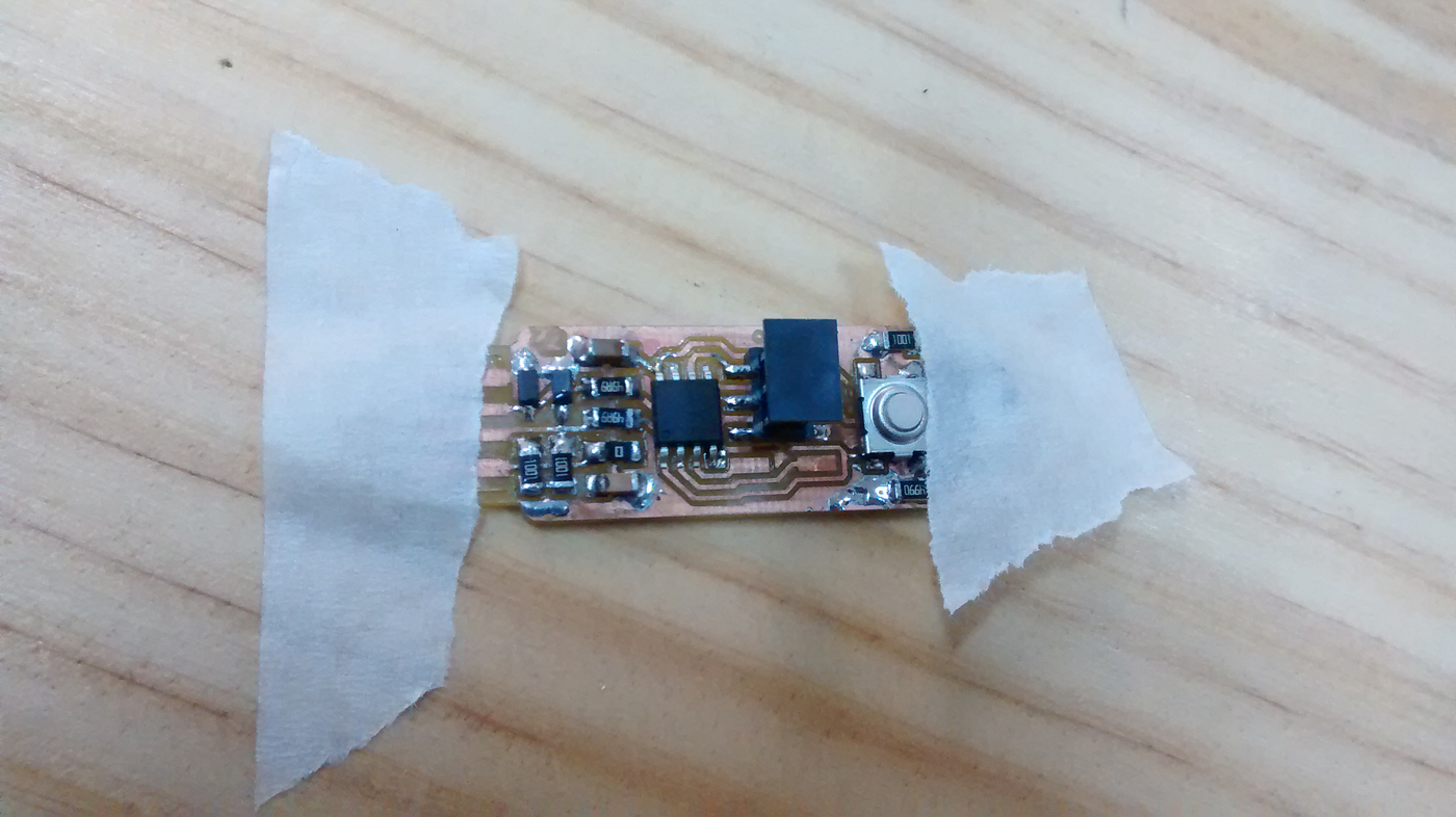
With the last consideration on mind, I started populating the board until done.
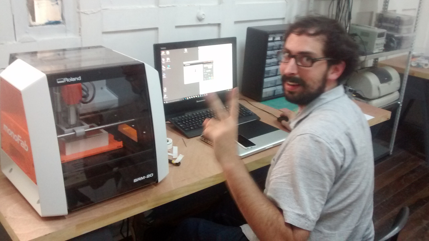
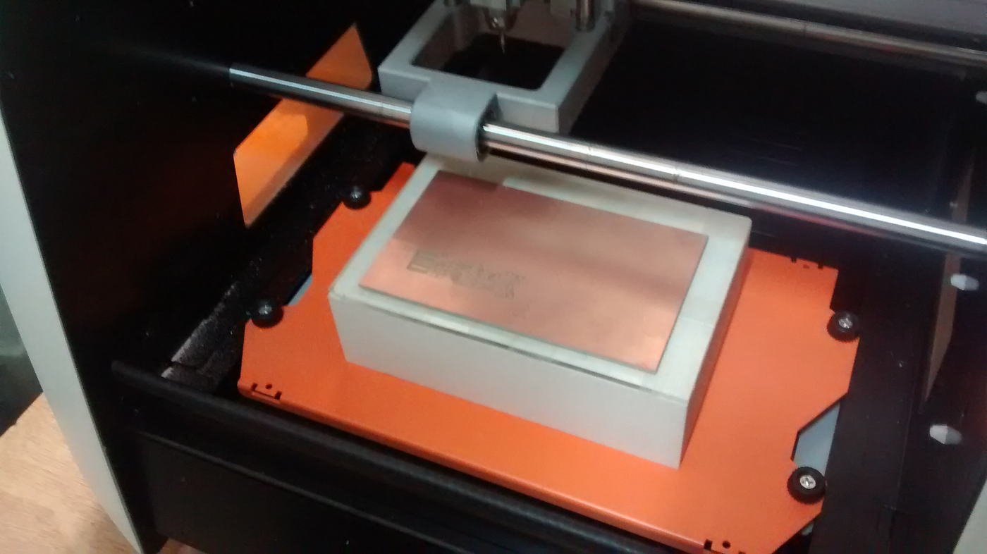
With Pedro (#391, on the pic) we setted up the machine. The first thing we noted is that the SRM-20's tray is way below the spindle, so we placed an auxiliary brick to rise the PCB board to the bit's reach (maybe the distance between the spindle and the tray is to avoid the machine's self-destruction!).
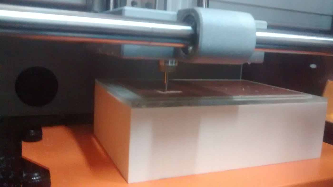
After rising the PCB, we moved the splindle to the desired XY position on the left-bottom corner and setted the X0 and Y0 positions. To set the Z-axis we placed the bit in the spindle and tighten it, then move carefully via software the bit to the surface (we were working with the 1/64 bit, a very thin and breakable bit). Once we were close, we just loosen the bit from the spindle to let it fall to the surface and, finally, tighten it again. Then set Z0 to 0.
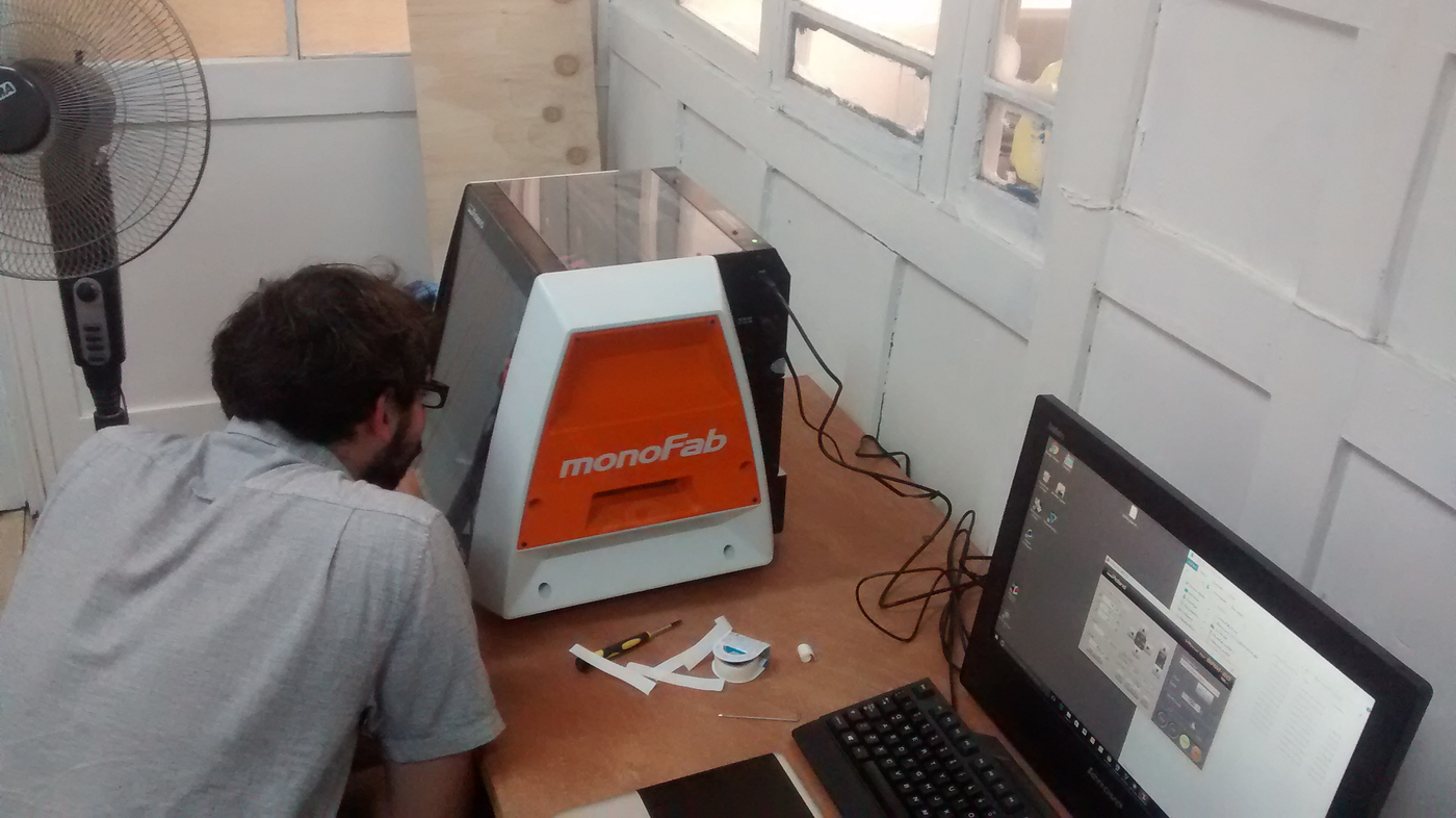
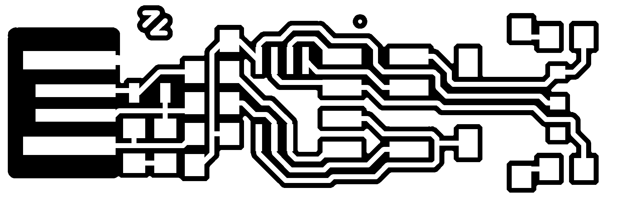
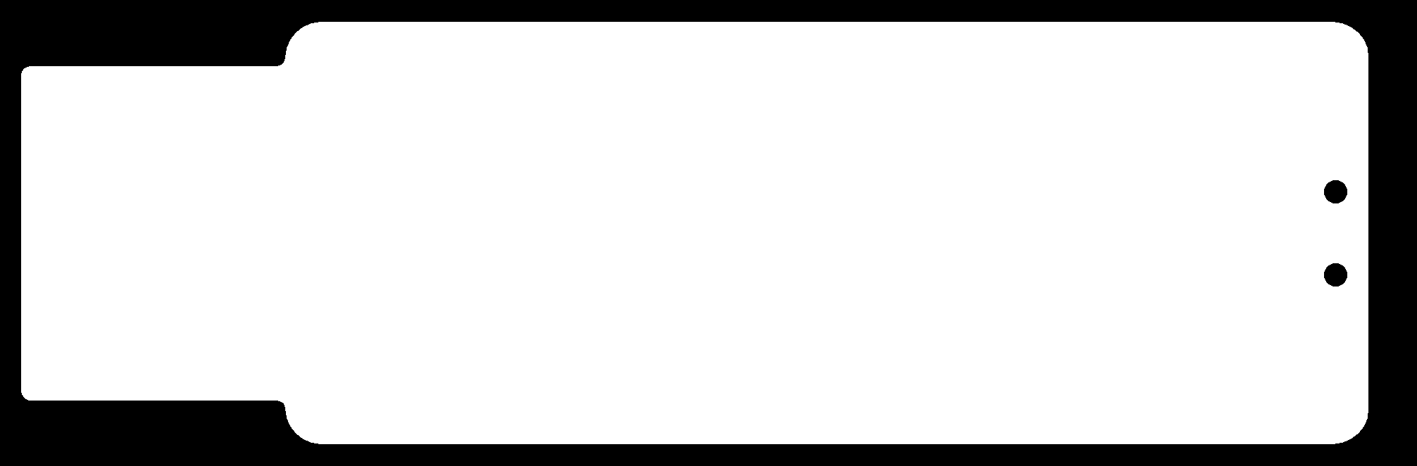
At this point, we were ready to start milling (the whole setup was very easy!). Of course, the first milling was the top image, and then the border
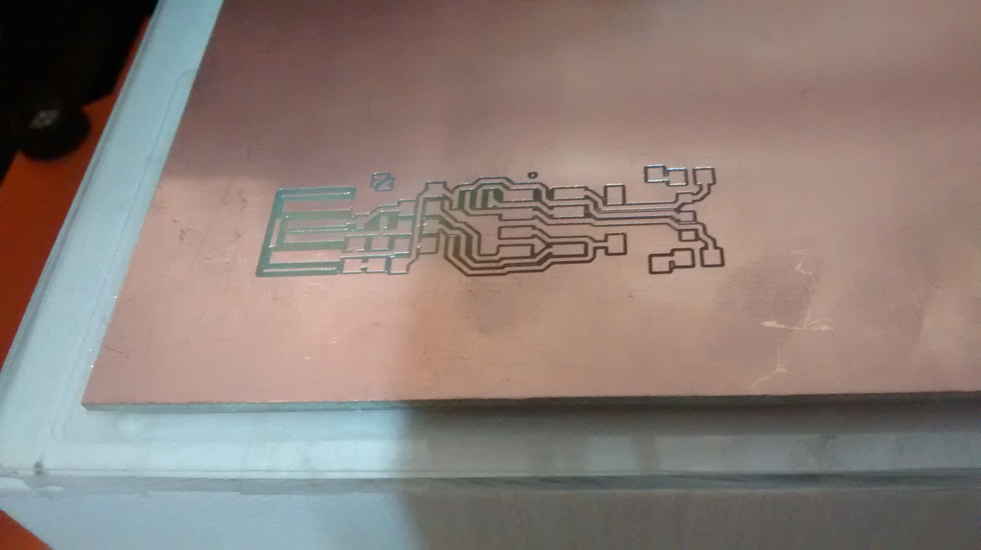
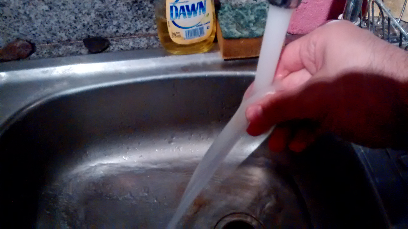
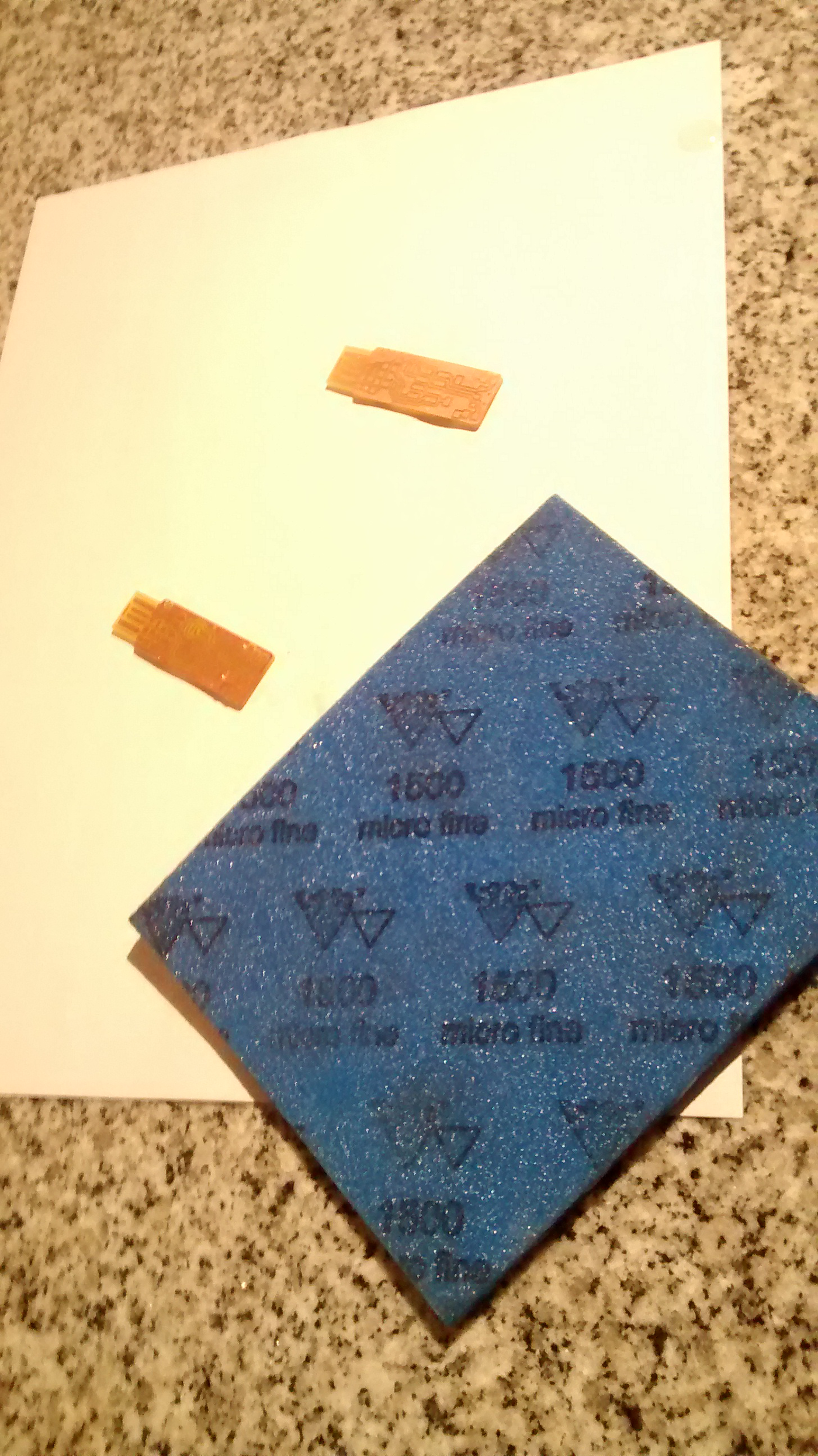
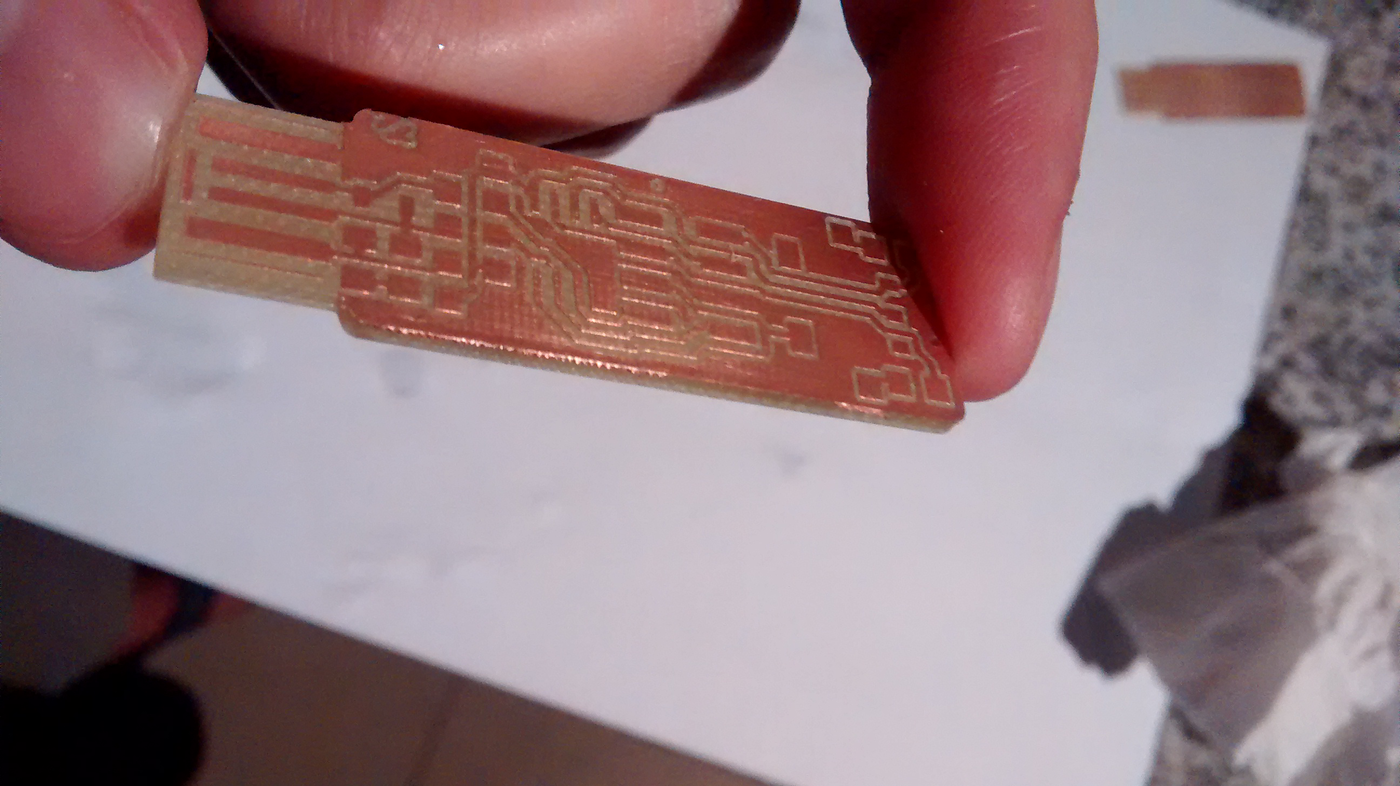
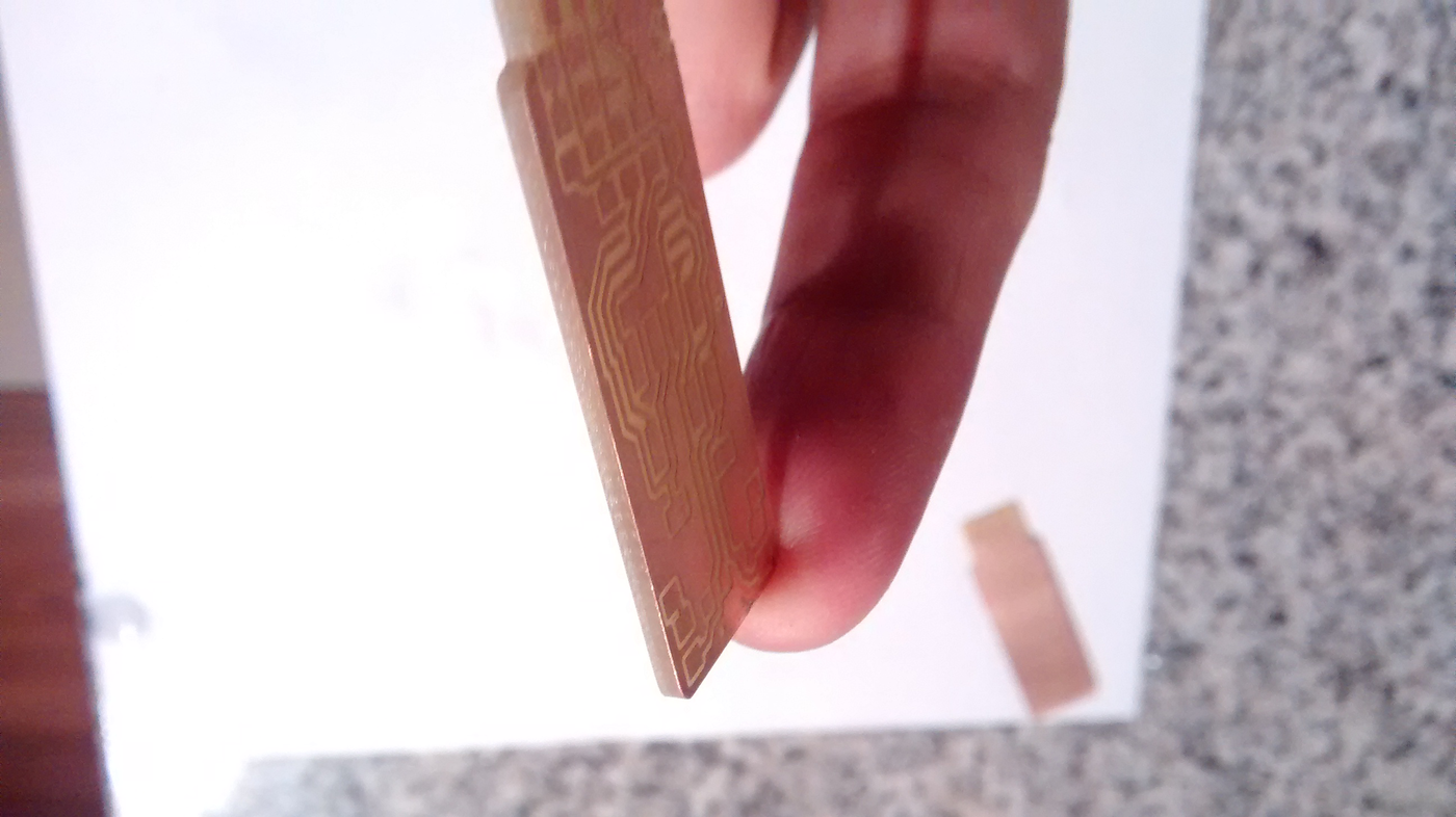
After milling the PCB, I proceeded to wash it and to softly sandpaper it to remove all the edges. Note the the edges on the sides needed an extra sandpaper pass. But finally, the board was ready to solder.
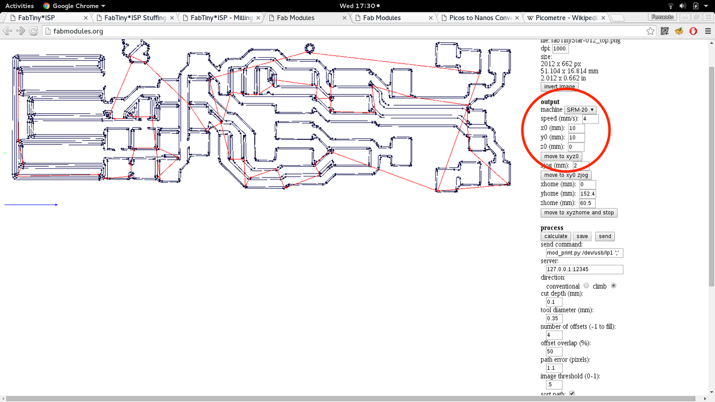
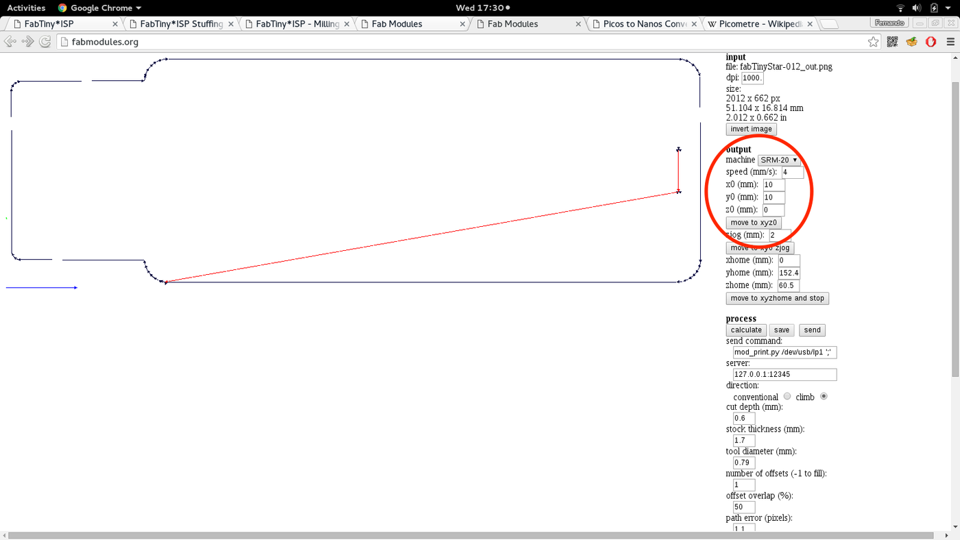
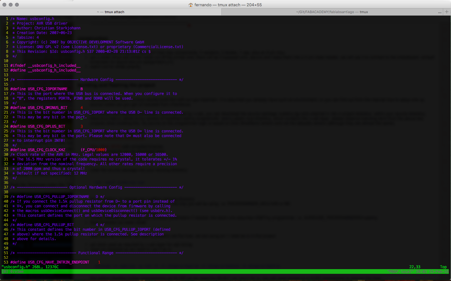
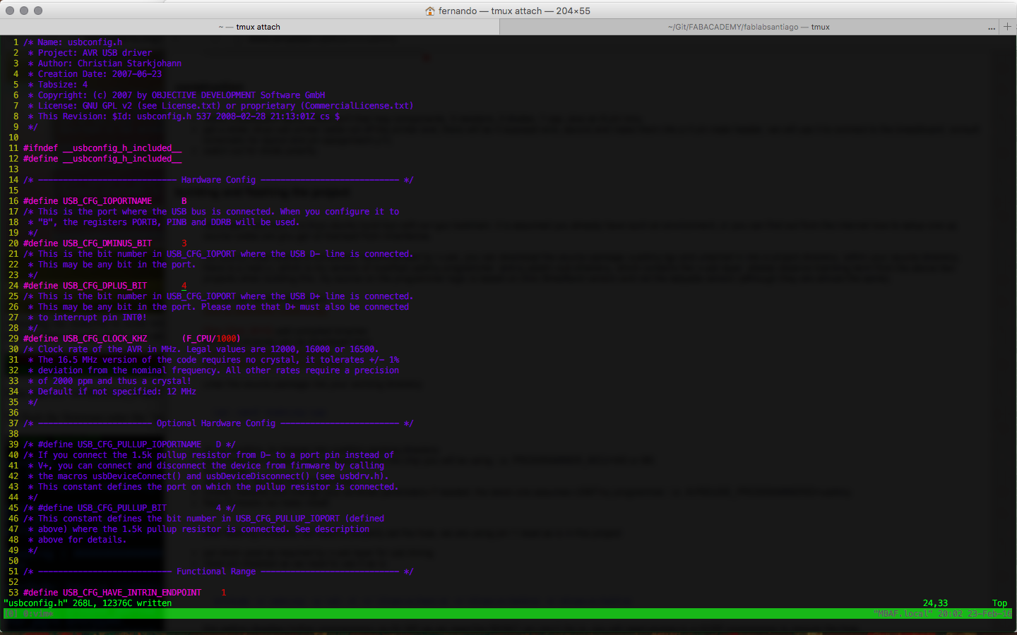
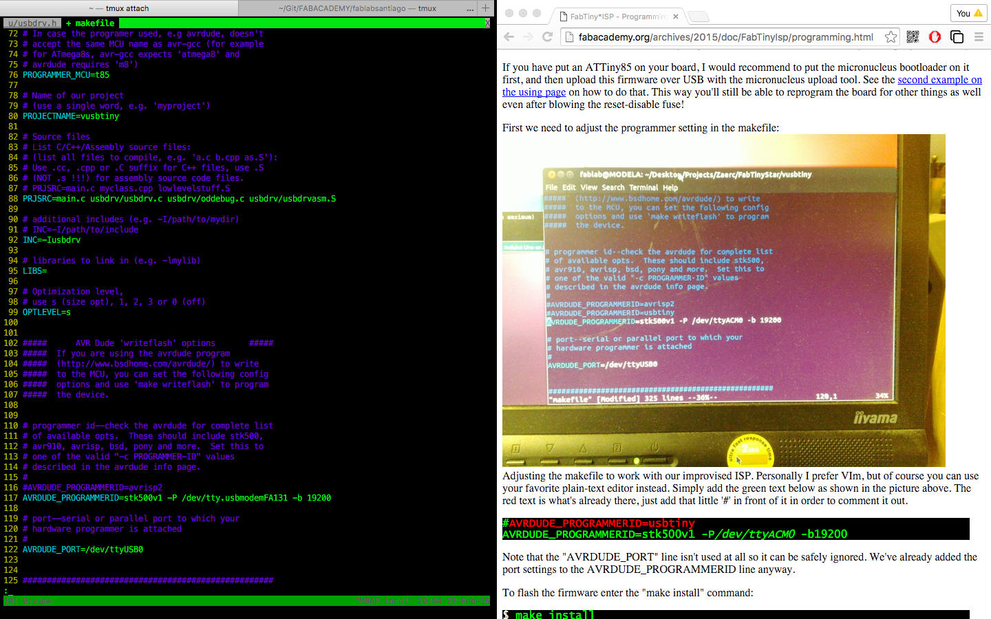
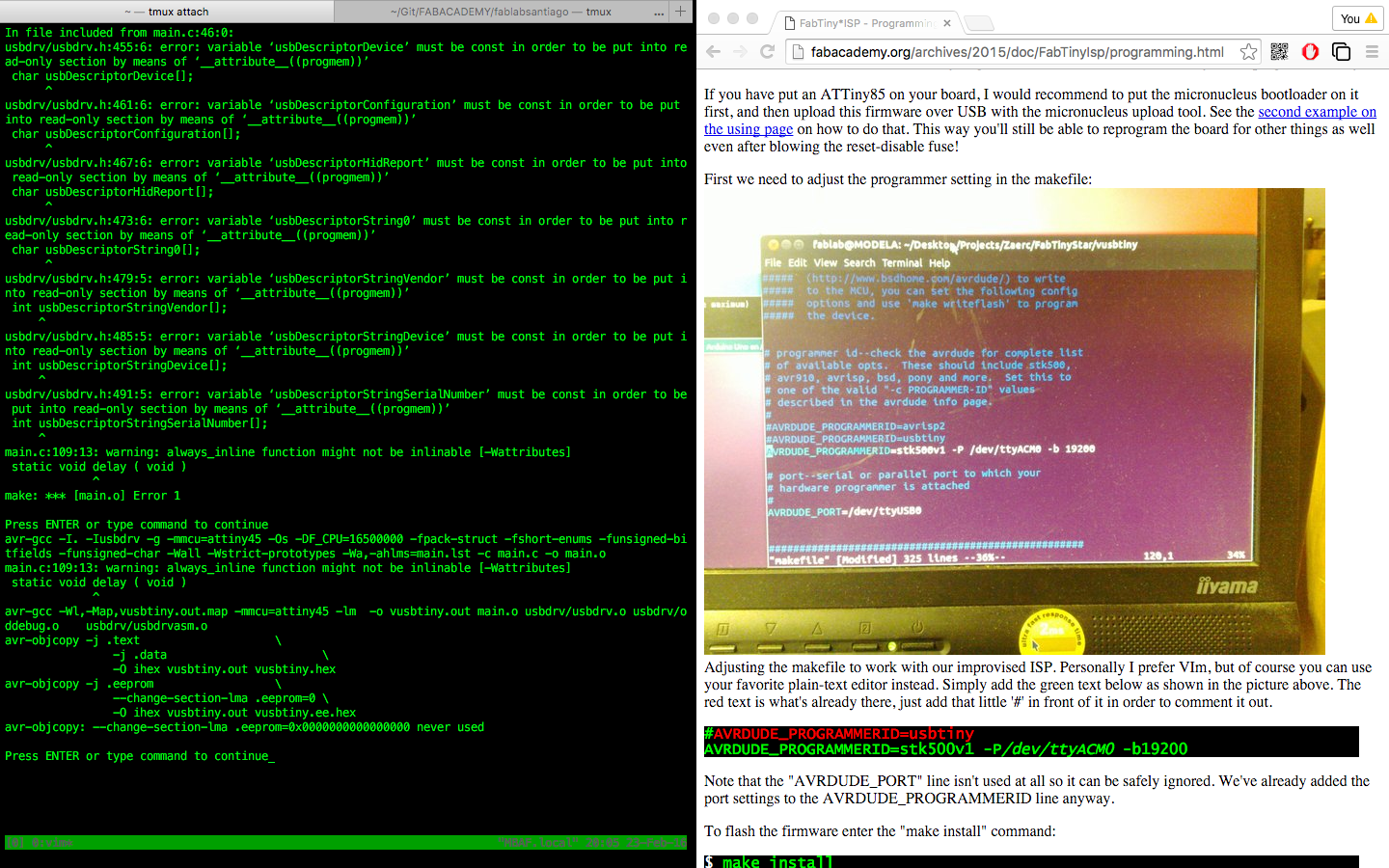
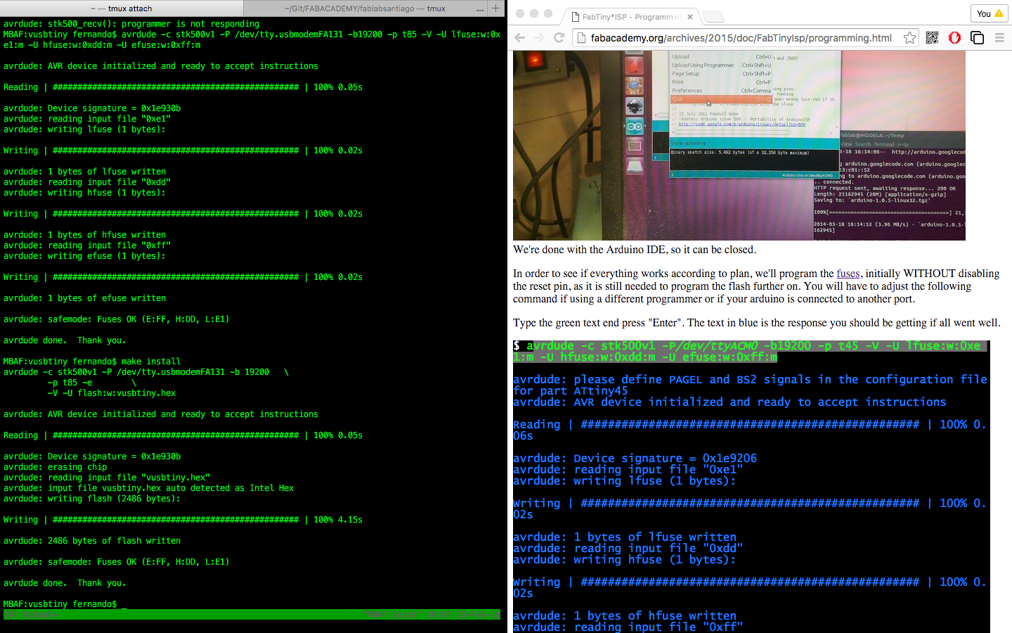
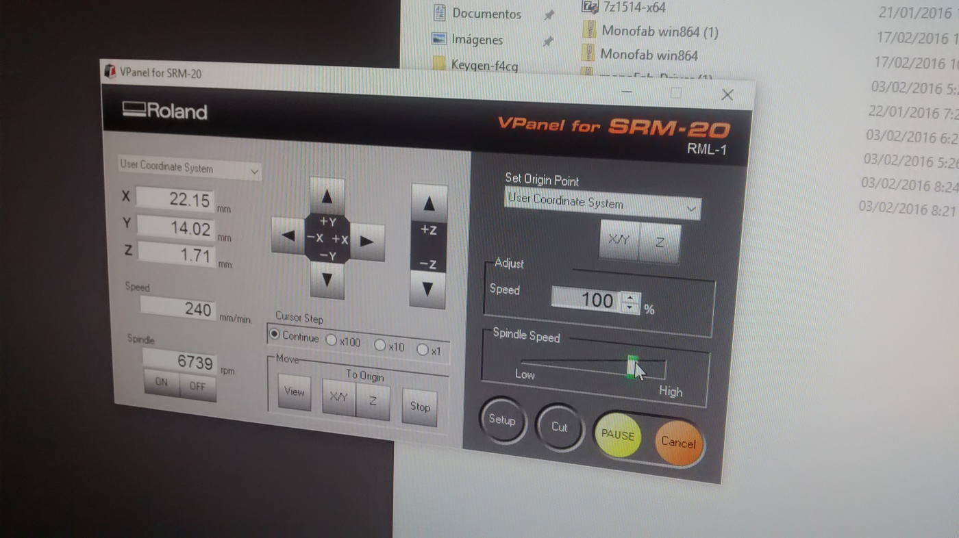
The first thing was to go to the fab modules site and load both PCB's .png images (top and border). I followed Zaerc's instructions with no problem at all; the only extra considerations (please note that in Zaerc's instructions he had to modify the bit's diameter in the 1/64" work to avoid and issue) were to set the machine to SRM-20 and to set the Z0 position to 0 (when I tried the website it loaded default values to all the X-Y-Z axis, and in the case of the Z-axis I moved it to the 0-level). Then I processed the work and saved to .rml files (top and border) to be run by the machine.
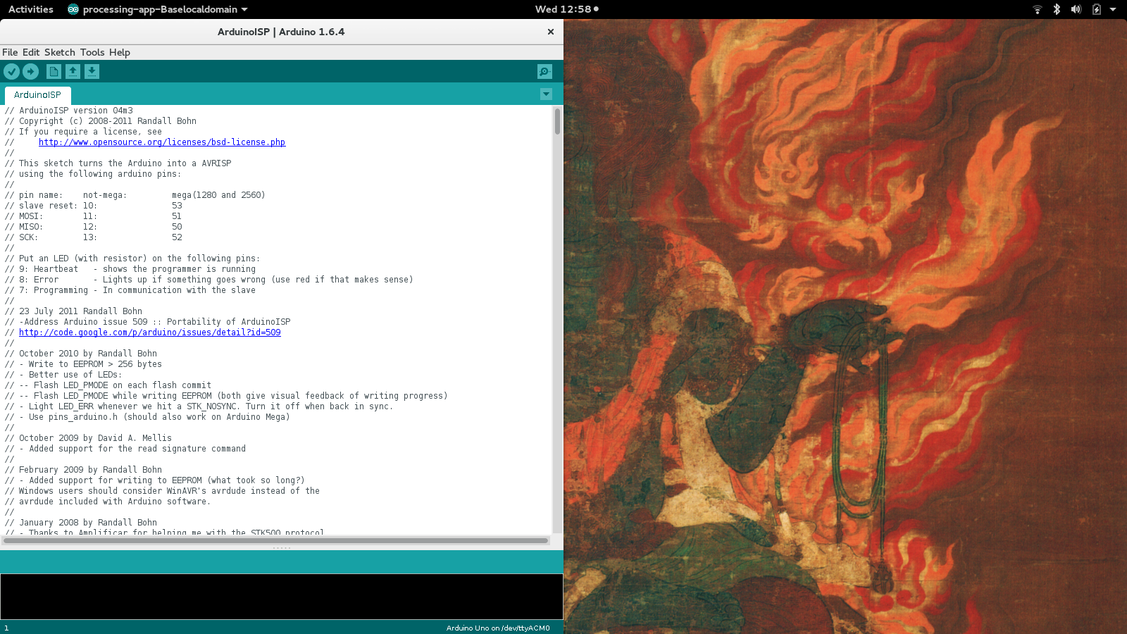
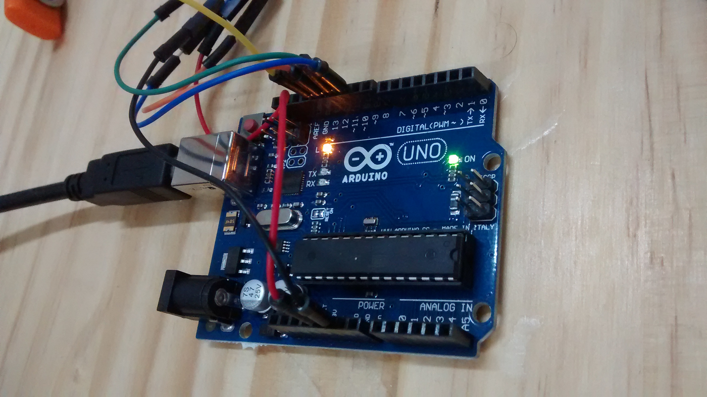
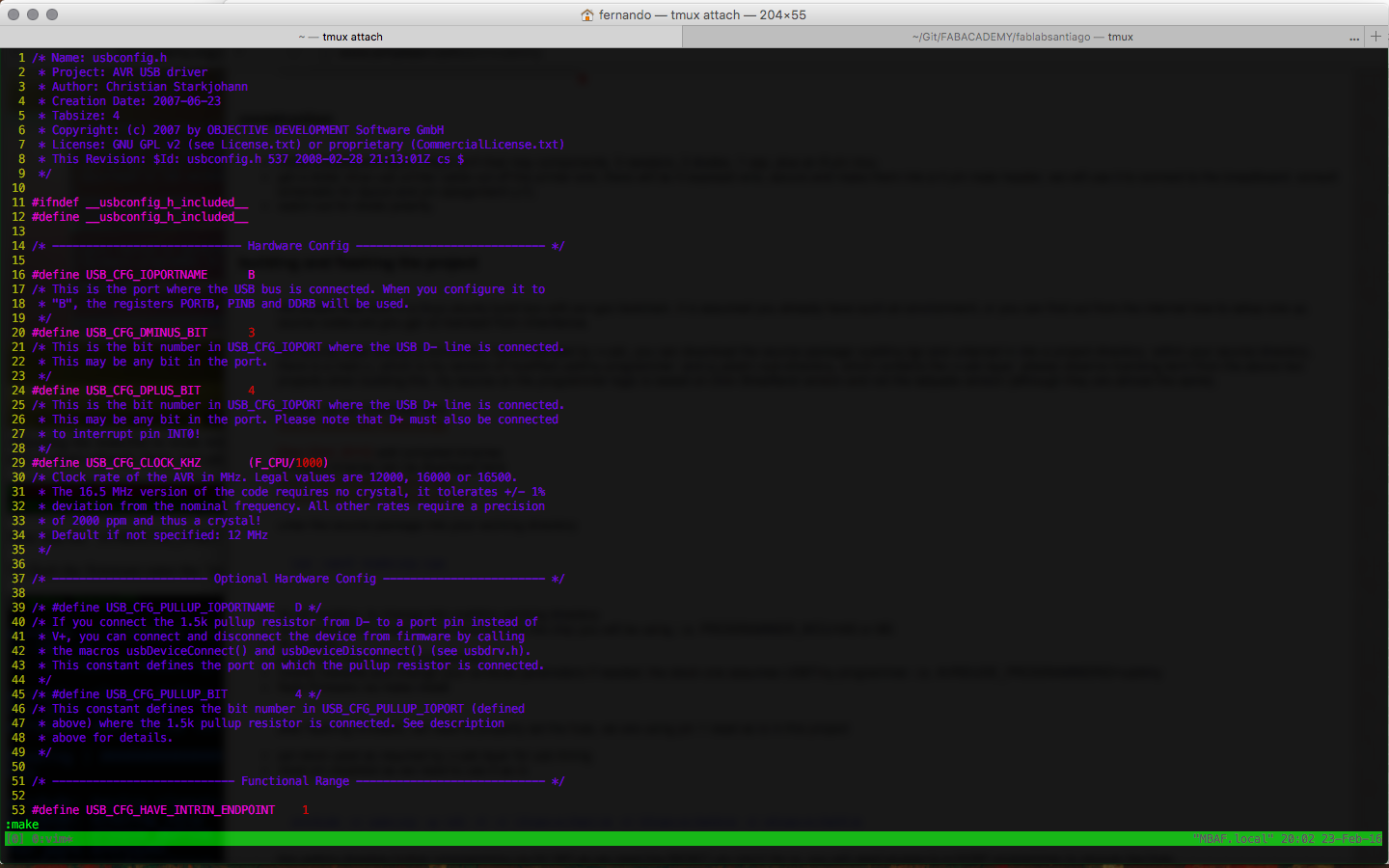
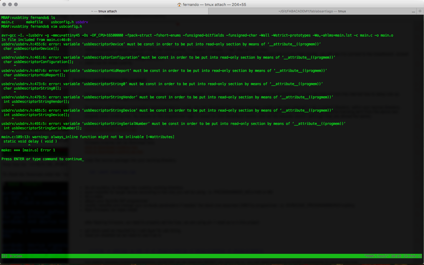
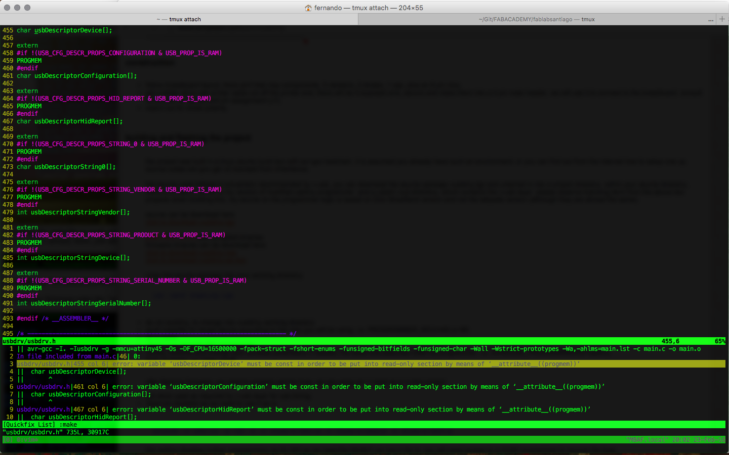
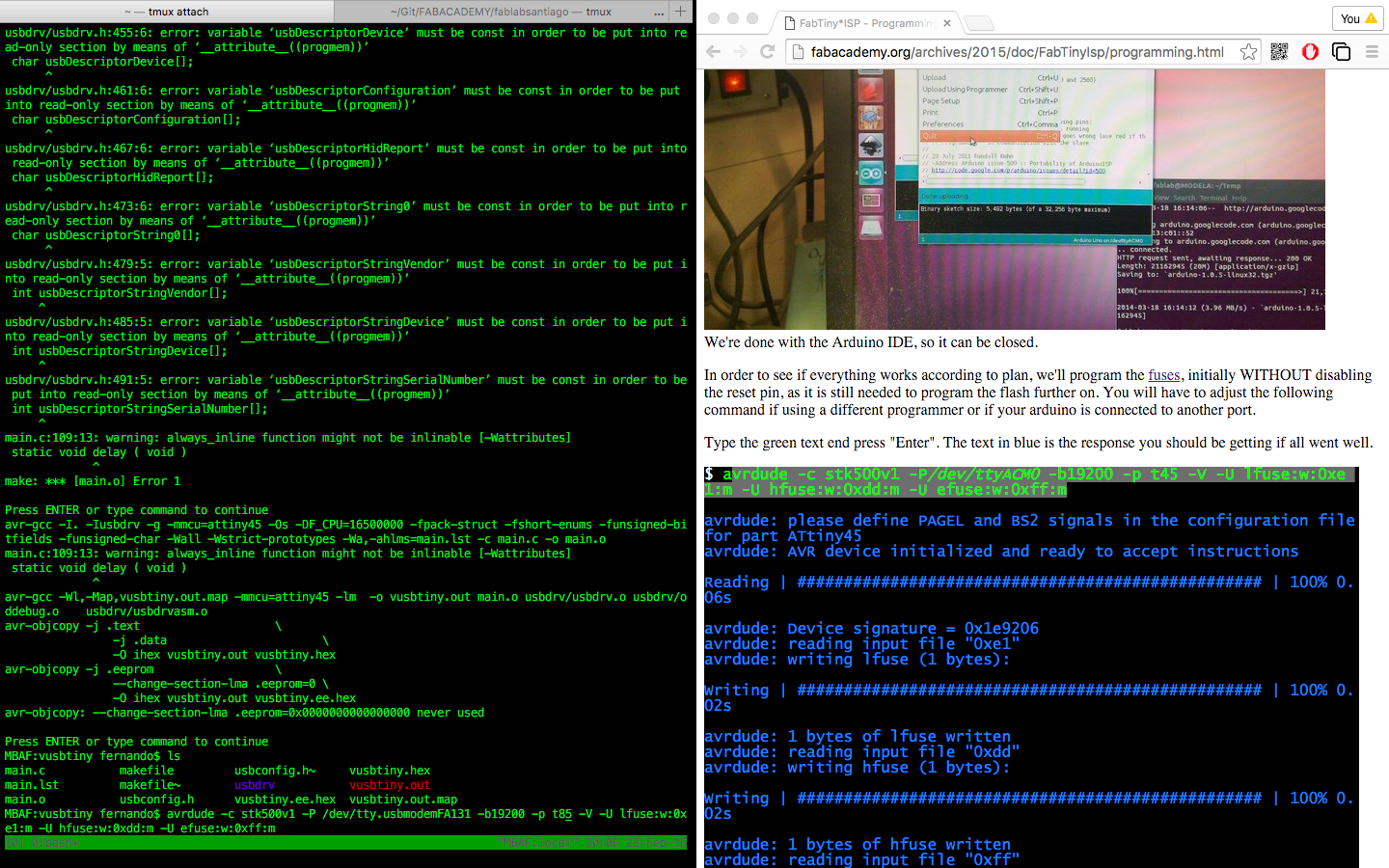
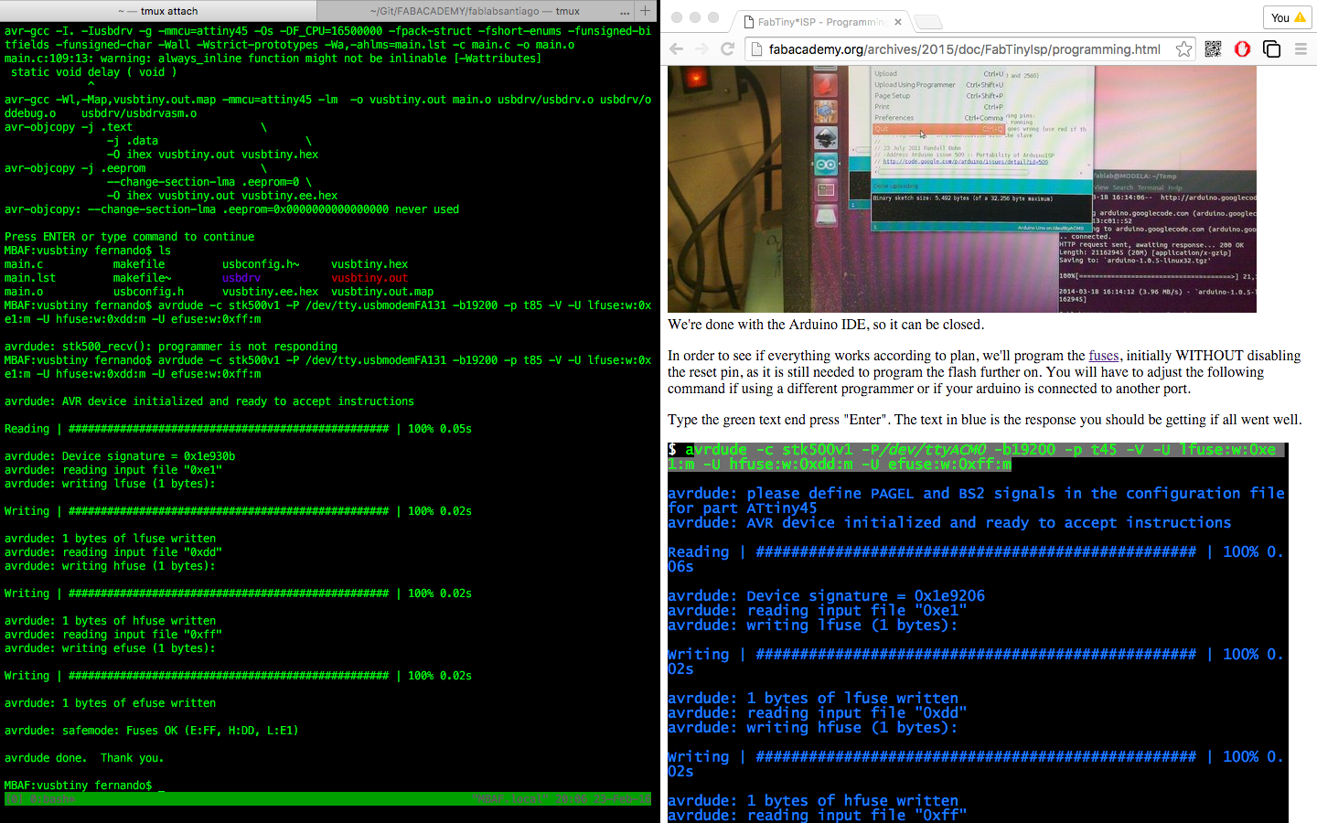
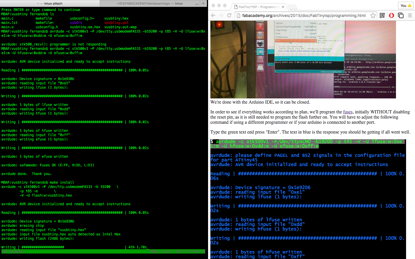
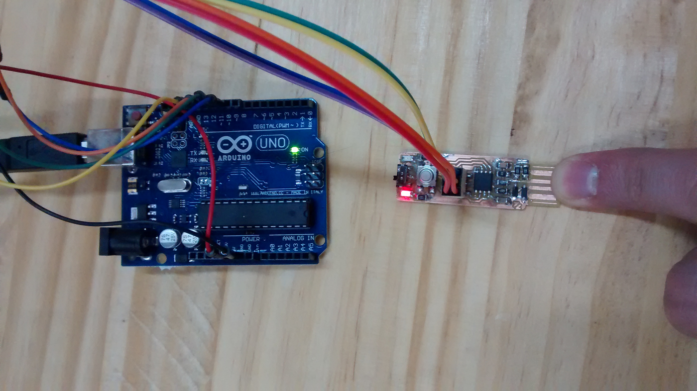
This week's assignment is to mill, solder and load up the firmware to obtain a ISP programmer. But there are options! So I reviewed the alternatives and chose Zaerc's version because it's extremely well documented.