Week #6: Electronics design
Our tasks for the sixth week were:
- Redraw the echo hello-world board we did two weeks before, adding at least a button and a LED
Since
I hate replicating something without knowing how it works, and also
since I love electronics (even though my knowledge in this field is
very limited), I chose to fully understand the schematic before
designing the board and milling it.
I found a really nice .PDF (file here, password abc123) from Atmel which really helped me through that. Ali's documentation was also helpful.
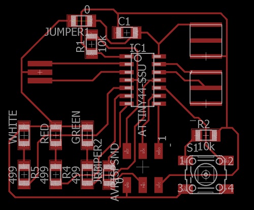
After
studying, I decided to make a board with 3 LEDs (white, red and
green) and a button. I tried really hard, but I could not manage to
design the PCB traces without using jumpers, so I had to add two.
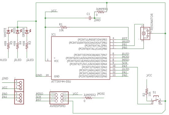
This is the schematic:
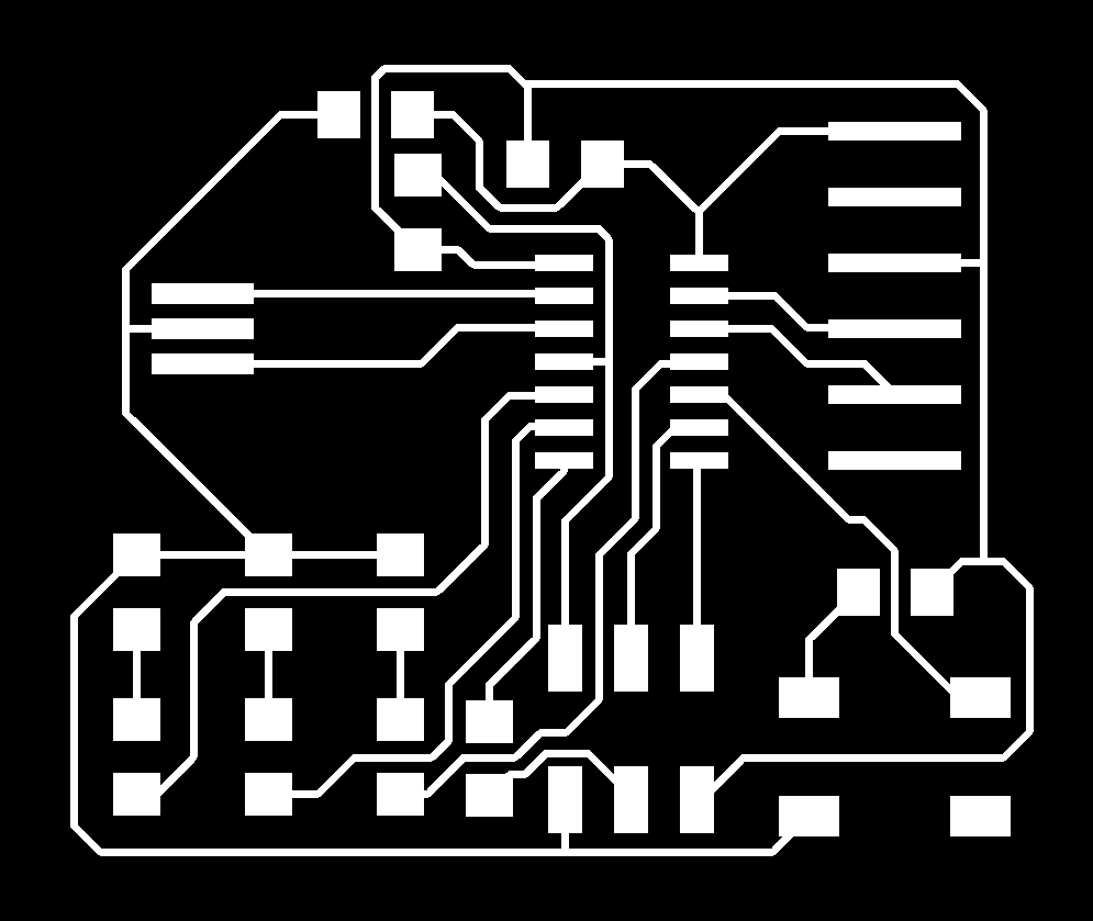
And these are the traces:
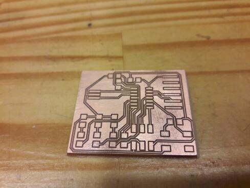
Then,
I proceeded to generate the .RML file using Fab Modules. But, before
doing that, I had to generate two .PNG files: one containing the
traces, the other containing the outiline, as can be seen below.

If
you want the .PNG files, you can download these directly, they are the
actual files in their original resolution. If you want the .RML files
generated by Fab Modules, you can download them here (password abc123).
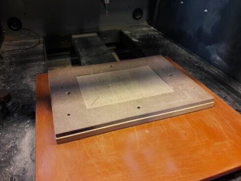
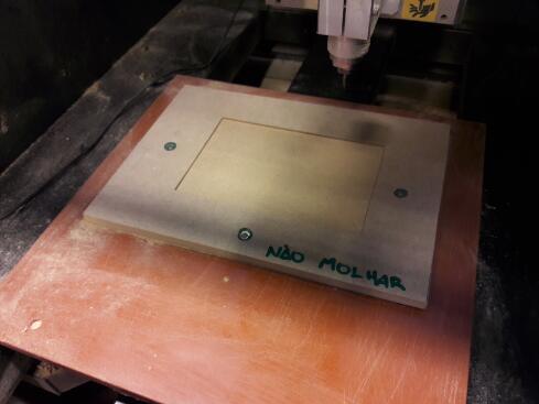
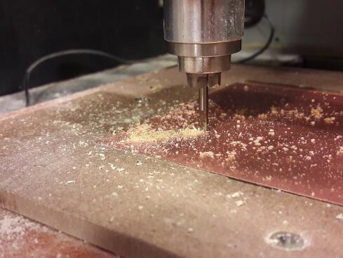
Then,
I proceeded to milling the PCB. Unfortunately, I made a terrible
mistake: when setting the xy origin, I did not notice it was set to G54
coordinates (another user profile), which uses a different file type
instead of the .RML. The result was that the machine "thought" the
origin was actually lower and the milling bit went deeper than it
should have; to make things worse, it did this at the very beginning of
the movement, which is a quick diagonal sweep across the board. It gave
me quite a scare and my colleague Daniel quickly intervened, pushing
the emergency stop button. This is the aftermath:
Fortunatelly,
the milling bit was not badly damaged, and it already was a little worn
out. So, I corrected the parameters and tried again, but the trails
were really, really thin. After trying 3 more times, a colleague of
mine told me that the table was misaligned and should be realigned (not
because of my accident, apparently someone had noticed it come days
before).
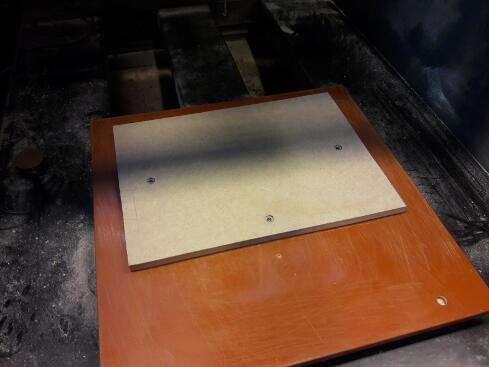
This was the old table:
Even
though this was a set back, it turned out to be great, because I had
the opportunity to learn how to align the table. After cutting a
rectangular piece of MDF, all we had to do was firmly attach it to the
machine and mill a filled rectangle. It took us a while, but this is
what we got:
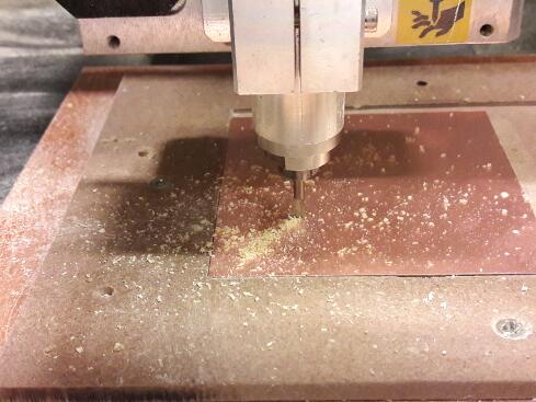
After we were all set, I proceeded - again - to milling the PCB. This is what I got:
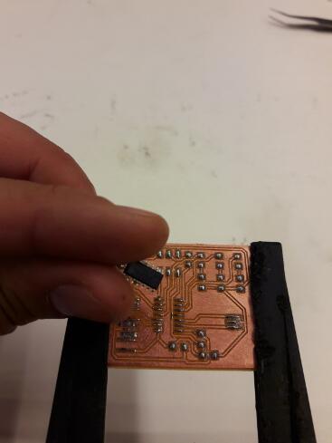
I first tinned all the contacts. The first component I placed was the Attiny 45:
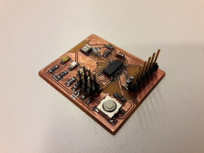
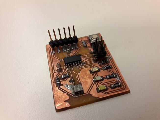
After soldering all the components, this is the final result:
Now,
all I had to do was to test the designed PCB, which was Week #8 assignment.