Electronics design

This week's global lecture covered electronics design. In addition, Emma gave an illuminating local lecture on electronics and using EAGLE software for schematics and board design.
About electronics
What is a schematic?
- A schematic in electronics is a drawing representing a circuit. It uses symbols to represent real-world electronic components.
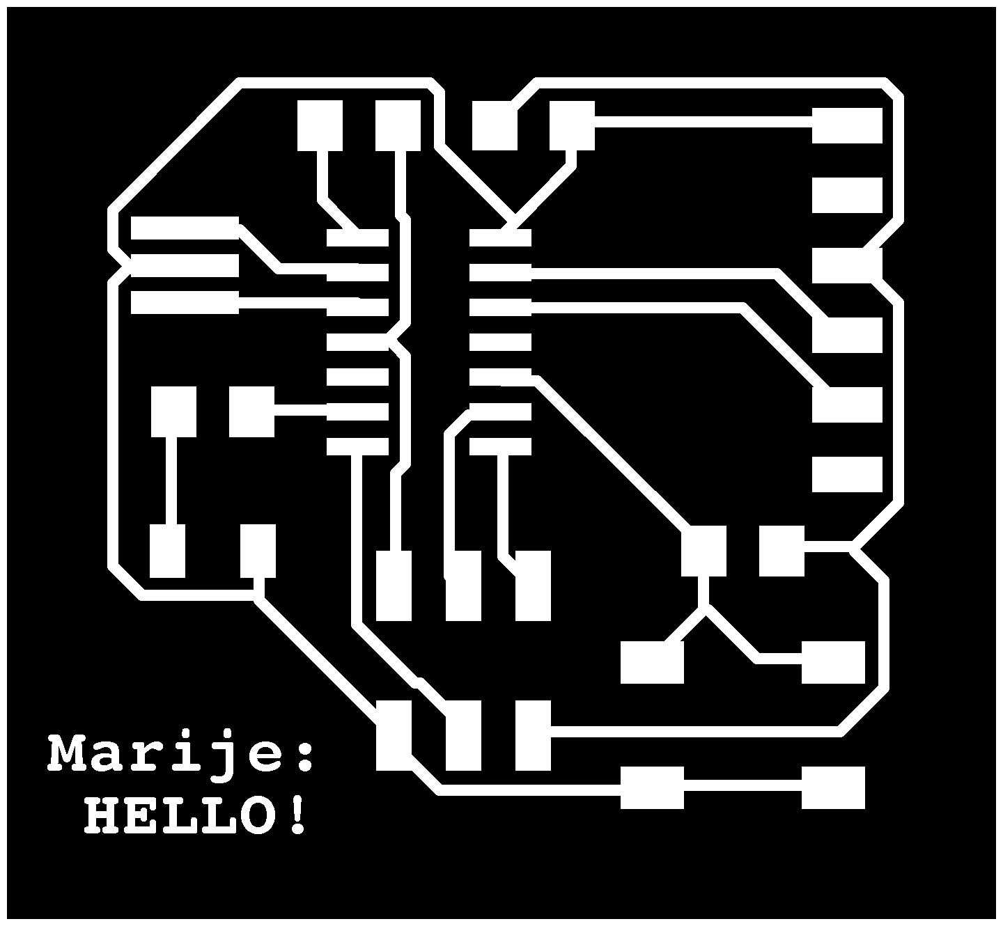
What is a board lay out?
- The board layout shows how the electrical componets and traces will be laid out on the board.
Basic concepts:
- I= CURRENT is the directed flow of charge through a conductor
- V= VOLTAGE is the force that generates the current
- R= RESISTANCE is an opposition to current that is provided by a material, component, or circuit.
Ohm's law formula / Equation:
I=V/R
- I= Electrical current, measured in amps (A)
- V=Voltage, measured in volts (V).
- R= Resistance, measured in ohms (Ω)
shows that:
- If we increase the voltage, the current will increase
- If we increase the resistance, the current will reduce.
Assignment
For this week's assignment, I worked on:
- redrawing the Echo Hello-world board
- adding a button and LEDs (with current-limiting resistor)
- checking the design rules,
- and making it.
Useful tutorials
To gain a more complete understanding, I also went through a couple of video-tutorials:
- General tutorial 1 for Eagle: Schematics Design
- General tutorial 2 for Eagle: Printed Circuit Board Layout
- This video shows how to use 'Net class' and 'Autoroute' to set the width property of the traces on the layout view.
- Short video tutorials explaining EAGLE
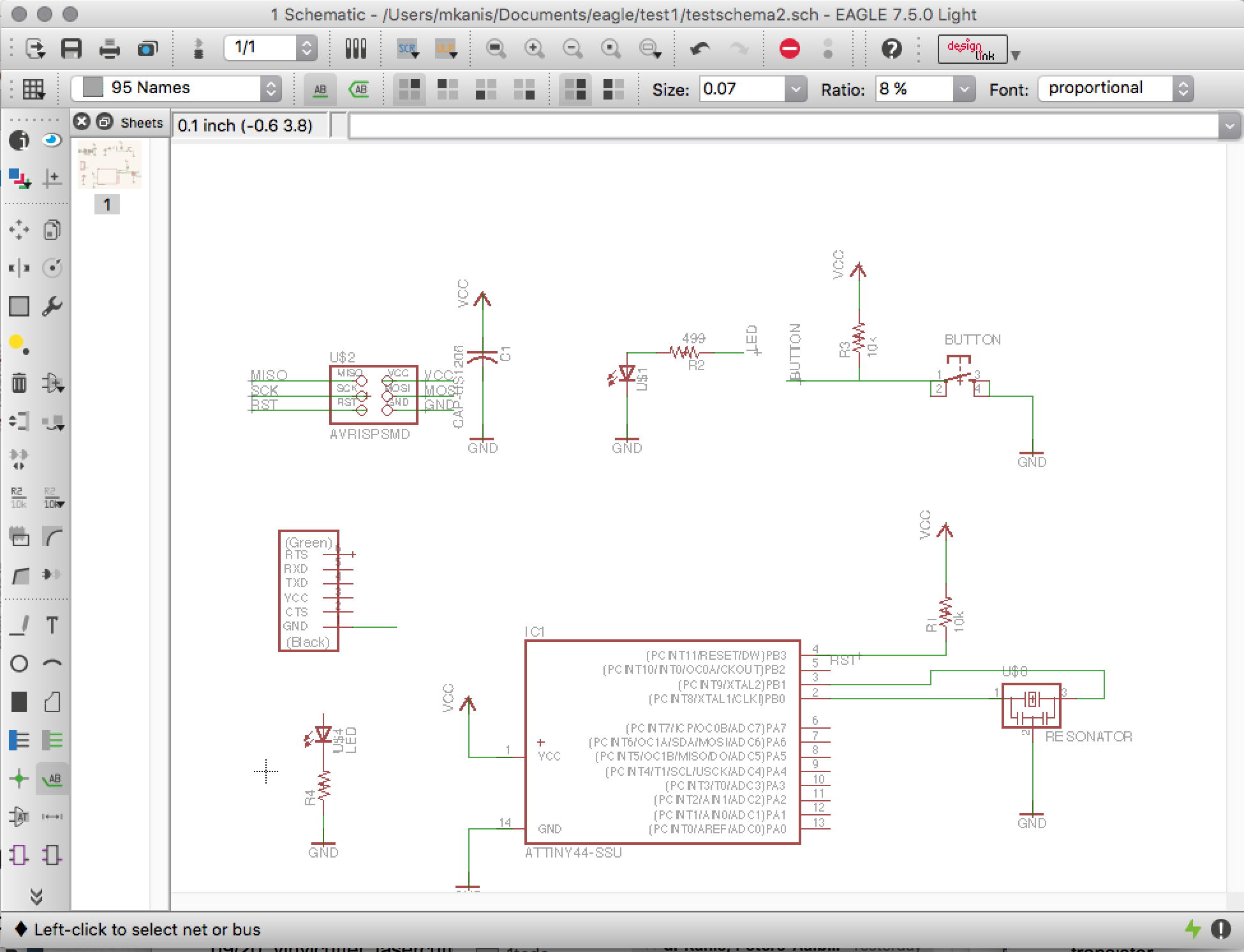 Hello-world board: Using EAGLE
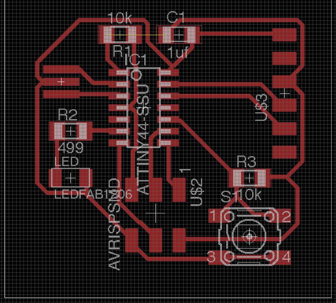
For the design of the hello-world board, which we needed to create, I picked EAGLE (light, freeware edition for the Mac) and used the tutorial specific for the weekly assignment to work with. After downloading EAGLE, I created a project, both with a file for schematics as board design. It is important to stress that these two files are/should be connected to each together, for not to have a 'broken board'. If the link between these files is broken (such as happend in my case), in the control panel, you can delete the board design file, and EAGLE will ask you to create a new one (you will however then lose the work created in that particular file).
Adding and using the Fab and Fab tiny library in Eagle enabled me to pick the right (1206) components, such as switches, avalable in the Fablab. I used the wire tool to connect the components. For redrawing the circuit, I basically followed the one in the tutorial using nets. The FTDI Header is different than the one used in the example, but as long as the lines are connected to the right numbers, that should be fine.
For the design rules (a list of rules that you want your layout to respect, such as width of and distance between traces) I used the fab.dru file for the Modela as found here. However, I changed all the numbers in the Clearance tab to 0.4. You can run the Design Rules Check (DRC) command to check the compliance of the rules. For the Net classes settings I used: Width 0.4 mm (Drill 0.8mm) and Clearance 0.4 mm.
Using the 'Ratsnest' command first to make efficient air wires (the yellow connecting lines), I ran autorouter to route the traces (strongly believing that is what a computer should be good at), while also exploring and tweaking the manual way. In the end, with Autorouter I obtained a 100% routed file. The result looked good, the only main difference was that the routes did not have 90 degrees corners, as this is not the more efficient way. Pleased with the result, I explored with adding some extra components (LEDs, resistors,...) and a ground plane using the video tutorial instructions. However, in the end EAGLE crashed, crashed and crashed some more up to a point that I lost lots of hours and I was not able to do anything anymore with the program. Suspecting that my files had somehow gotten corrupted, I deleted my latest EAGLE files (particularly the .job files) and started all over again. Still, the program continued to crash. I discovered that changing the Routing grid (final setting used: 0.403) was very crash sensitive, so I left that untouched and decided to continue using an earlier saved version (without the fancy bits such as ground plane) thinking this was still perfectly fine... and prepare these for milling.
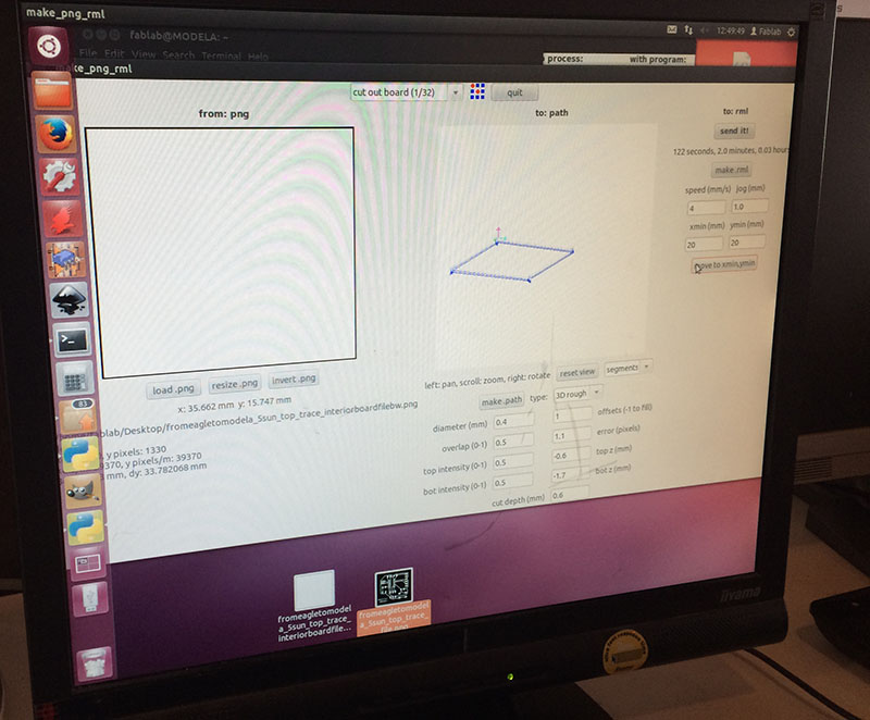
 For preparing the file for milling with the Modela, I chose Export Image > Monochrome, 1000DPI, full area. With GIMP I created an extra file for cutting the board (using the 'fill paint' tool, adding a 20 pixel even white border to the Canvas size and using the center command). I also added a personal text, which was small (as I did not want to waste extra copper), using Bold text and extra indent spaces beteen the letters. Just to be sure, I checked (in Photoshop, with 'Image size') to make sure the Trace file had the same dimensions, while also inverting the cut file (It should have a white border with black on the inside). Although the text and board was very small (a soldering challenge!), it came out well.
Tips
- Use "add" to open up the libraries so that you can add components in schematic view
- 'Value': adds value to components (i.e. Ohm rating)
- 'Name': names a component in schematic view
- 'Label': will display the name of a component in schematic view
- Moving the (bigger) components is easy, just make sure you also CTRL click (on Mac) on the plus sign
- Use Tools > ERC to check for potential errors in the schematics design. You can probably ignore most warnings. However, make sure all lines are well connected
- You can also use the 'Move' and Junction tool to make sure and check whether the components are properly connected with the lines (wires)
- Enter 'ripup;' in the command line (from board) to unroute all autorouter traces in one go
- In Autorouter, you can pick the Via shape: Round or Octagon
- In Autorouter, pick n/a for 16 bottom, as not to create a double sided board (and create via routes).
 Milling the board
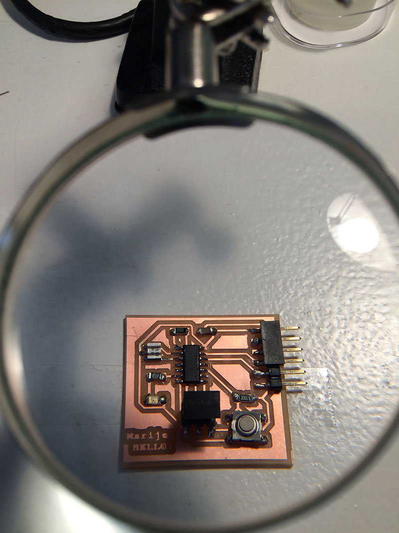
Milling the board with the Modela was similar to when creating the FabISP in week 4. Make sure to use the 1/64 end mill setting when tracing and 1/32 when cutting the board. As initially the Modela did not cut through the copper board, we changed the Diameter size and rerun the job (moving from the same recorded starting position).
 Populating and testing the board
Putting the components on my tiny board was a good exercise to practise my soldering skills again. In Eagle, you can use the 'Show' option to display what traces should be connected by clicking on the in-between lines. This is very handy, as then with the multimeter you can test whether these connections are properly soldered as these should. Although first overlooking that the top connections of the header component should be tested (instead of just the solder beneath), this process really helped to make sure the board was in order. Well, then to really make sure, I connected it with a FabISP to the computer (by first identifying MOSI using 'properties' in the Eagle board design, then connecting this with the right, blue side of the cable), which unfortunately did not work, as shown in the Terminal:
~ $ avrdude -c usbtiny -p t45
avrdude: initialization failed, rc=-1
Double check connections and try again, or use -F to override
this check.
avrdude done. Thank you.
 We found the reason was that a connection had gone missing in my original board design... Looking back, the 'before EAGLE crashes' file eventually used was less great than initially thought. Ah well, the creative solution was to add and solder a real wire. Then testing it with the computer using the same ~ $ avrdude command in the Terminal worked!
avrdude: AVR device initialized and ready to accept instructions
Reading | ################################################## | 100% 0.00s
 Files
Files


")


