Electronics Design
Goals
- Redraw the echo hello-world board, add (at least) a button and LED (with current-limiting resistor), check the design rules, and make it
- Optional: simulate its operation. Measure its operation
Eagle comes with a truckload of pre-loaded libraries (this boggles the libraries viewer quite a bit, but you can disable the ones you don't need, just toggle off the green dot next to the library name in the control panel), but the one we really need is not included by default, so we have to download and import it before being able to use it.
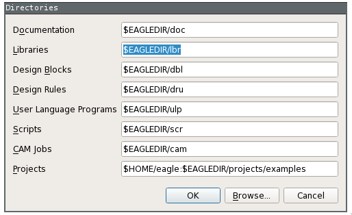
We have 2 ways to import a library, a manual one (via the "File > Open > Library > Save as.." route), or a more automatic one: if we take a peek at the control panel, under "Options > Directories" we can see where Eagle stores its files ($EAGLEDIR being Eagle's startup directory if you're running GNU/Linux)
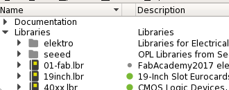
So moving our fab.lbr inside the "lbr" folder will suffice:
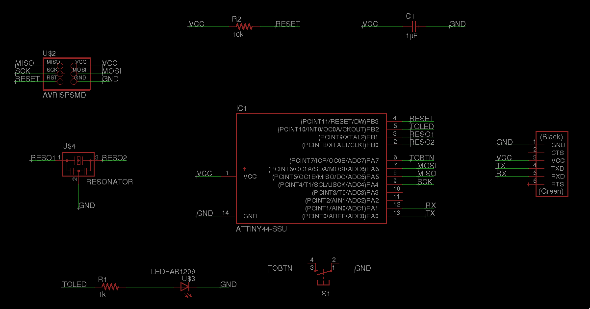
We can now open a new project and start drawing the schematic for our board; this is a 2 step process: first we add all the needed components, then we link them with the "Net" tool.
In order to speed up the process and avoid a mess of spaghetti-net, we can use the "Name" tool: just link a component with a net stump and name it, Eagle will keep track of every name and will try to connect all the identically-named nets
As a reminder of what is linked to what we can label each segment with the "Label" tool (you saw this coming, I know). A further way to visualize all the linked segments is the "View" tool: use it on any stump and all the related segments will be highlighted:
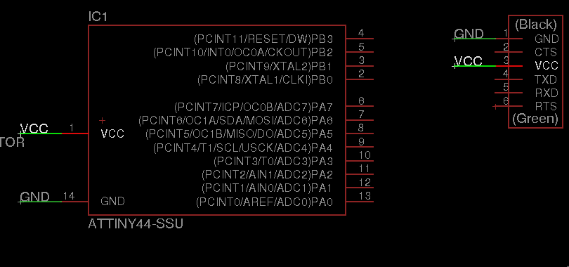
After a bit of clicking around you'll have your full schematic.
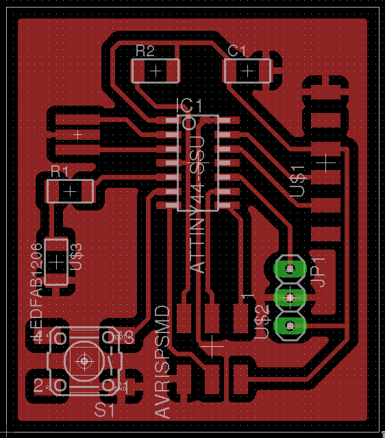
Now it's time to start working on the physical layout of our pcb: after switching to the board window we'll be able to see our components lumped together in an ugly mess: start moving them on the actual pcb plate, remembering that the free version of Eagle has some limitations (max 2 schematic sheets, 2 signal layers, and 80 cm2 board area).
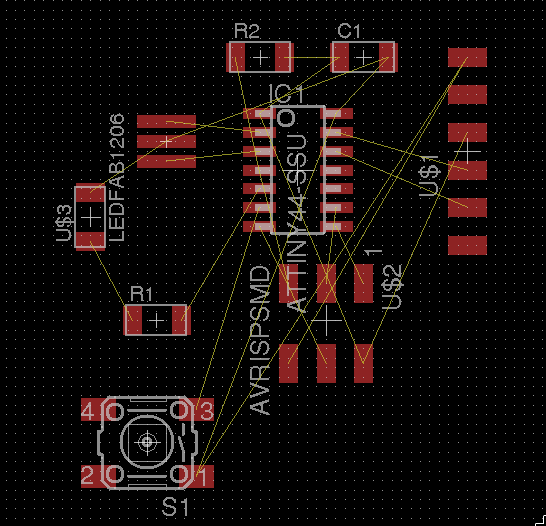
We can now start connecting the components (following the yellow airwires suggestions) with copper routes
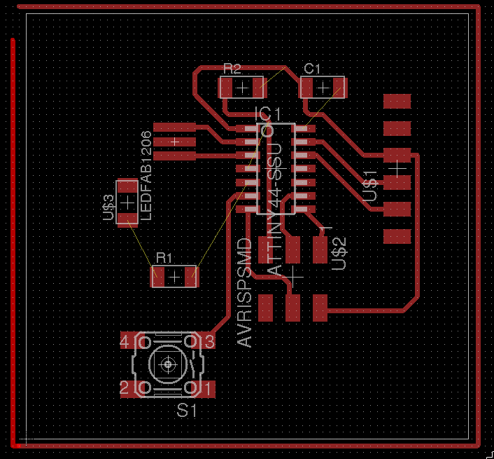
One neat feature is the ability to create copper pours: with the "polygon" tool we can draw a rectangle enclosing our board, then we can select and name it (with GND, in this case). After this we can refresh our view clicking on "Ratsnets" and our copper pour will be created, linking all our ground connections (more on this subject here, here and here)
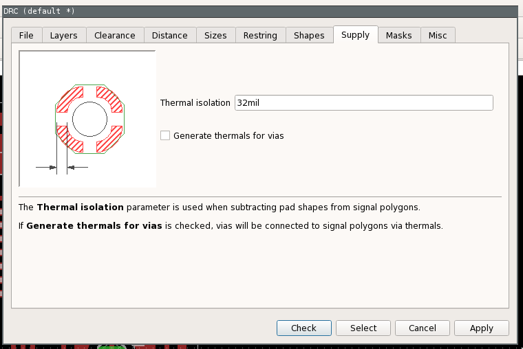
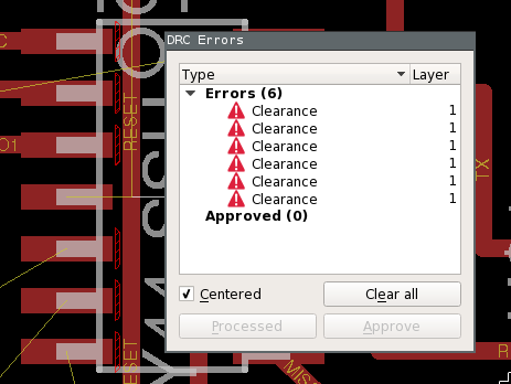
The last step before exporting the png to create the milling paths via fabmodules is to check our board for errors, with the aid of the "Design Rule Check" tool (DRC from now on). This tool lets us dictate several policies concerning our board (vias width, clearance between components, pads dimensions and many more) and checks our design for violations; these are my settings:
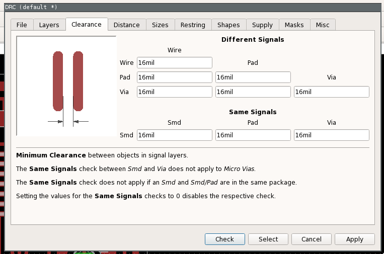
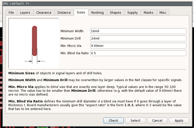
I chose to set my clearance to 16mil because the end mill of our SRM-20 has a diameter of 15,6mil (a mil being .001 of an inch). Alas, my reasoning was unsound and this led to a defective board (more on this later).
The DRC will highlight any error in our design, with a brief description of the problem:
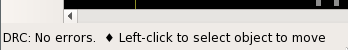
I dealt with all the issues, until the DRC showed a laconic "DRC: no errors" message in the bottom left corner of the window:
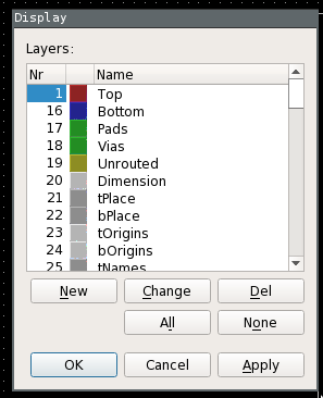
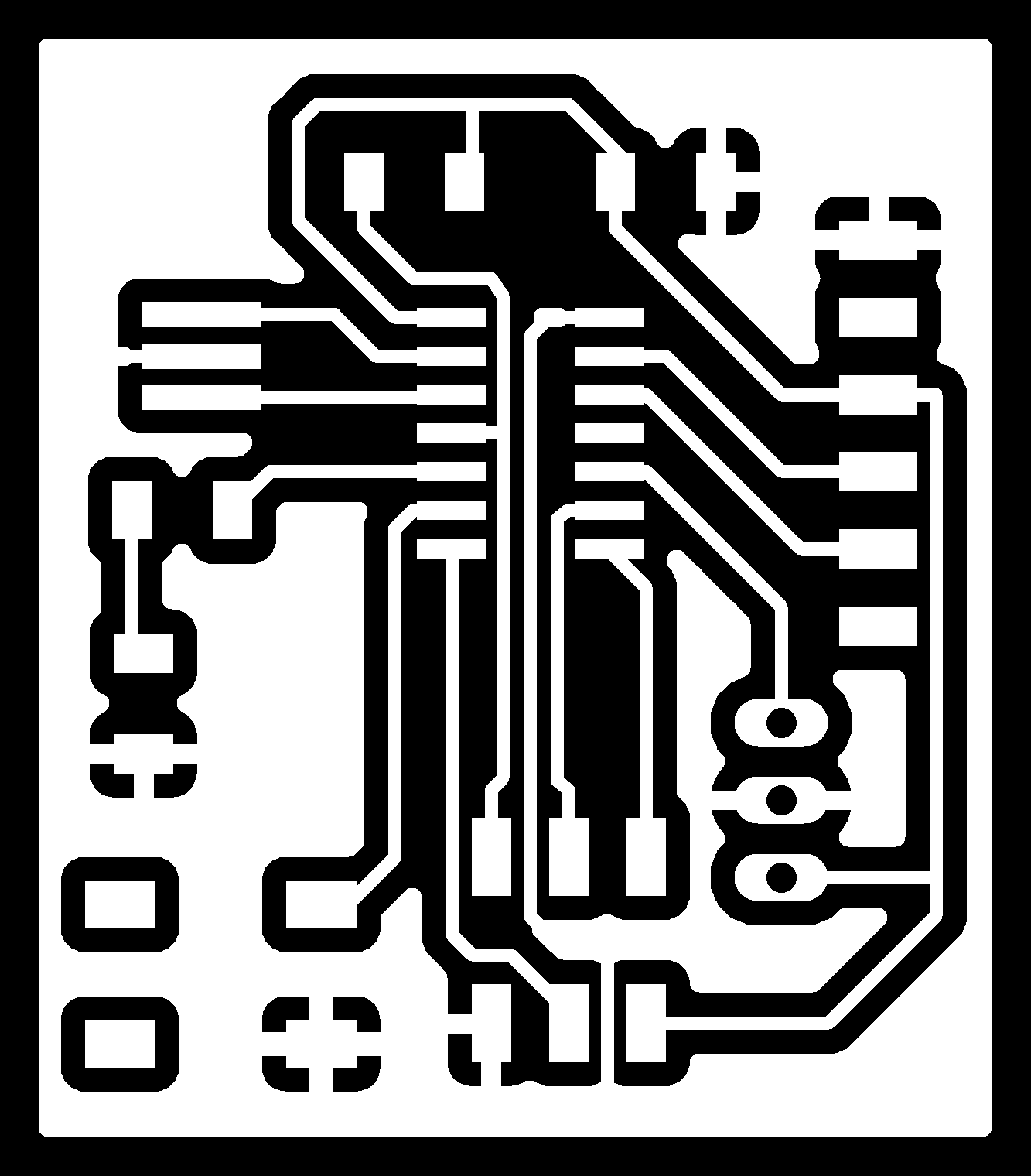
The last thing left to do was to export my board layout as a png, in order to feed it to the fabmodules and generate the .rml file for the milling machine. First I got rid of everything but the traces: I opened the layer editor (View > layer settings) and deselected all layers but the first:
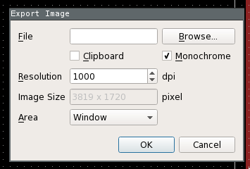
Then I went to "File > Export > Image", chose a file name, set it to be Monochrome, 1000dpi, area: window and exported my board
Creating the .png
In order to make the 2 .png files for milling (traces and outline) I used Gimp, following this workflow:
- Image > autocrop image
- Image > canvas size
- Add 100px to both height and width and center the image
- Create 2 new layers: a black one and a white one
- hide the white one, place the black one beneath the layer containing the traces
- Export as png to obtain the traces
- Place the black layer on top, and go to "Select > All"
- Shrink selection with "Select > Shrink", pick a suitable size (25px in my case)
- Delete the selection
- Export as png to obtain the outline
- Extra for drill holes: select the black holes in the traces layer with the Fuzzy Select Tool, invert the selection, delete everything, export as png


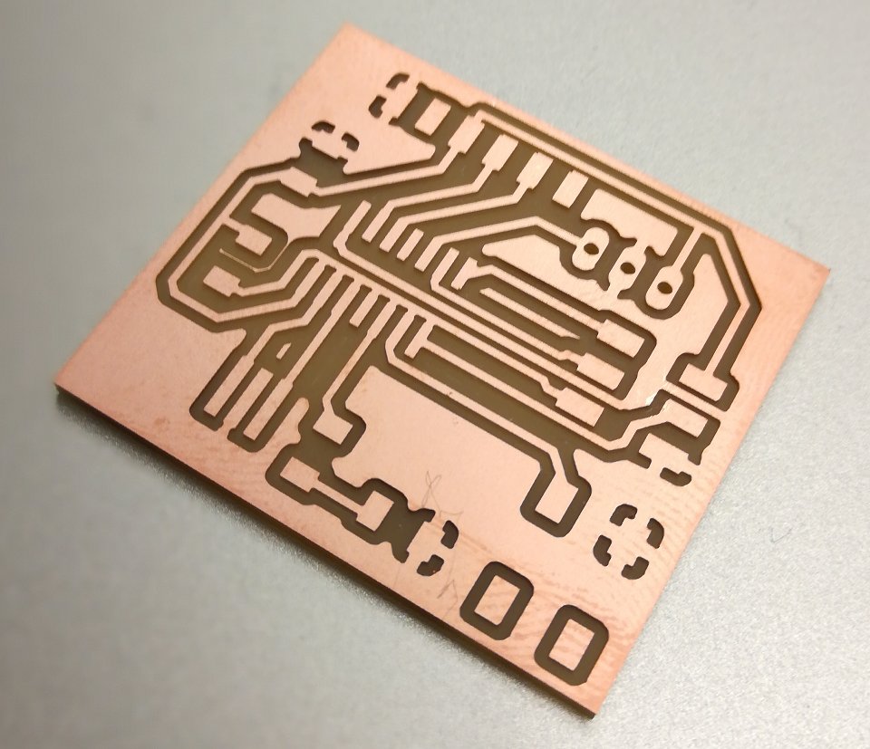
And you are ready to feed the images to the mods to get the .rml files for the milling machine (as illustrated in week 04; in this case the cutting order was traces (1/64 end mill) > holes (1/32) > outline (1/32)).
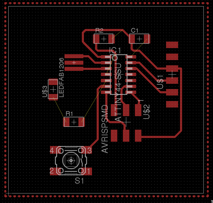
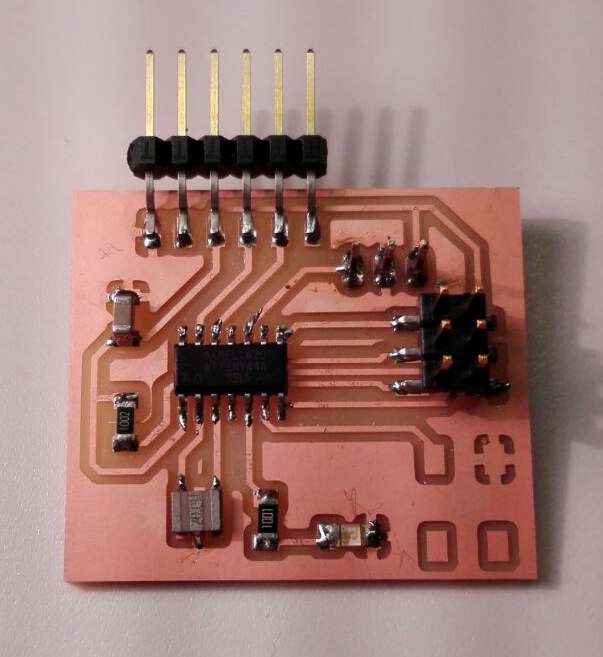
This was the final result; please notice how the attiny pads on the left side are still connected to the middle vias, leading to a faulty board. I noticed it only when I finished soldering my components, so I had to desolder the microcontroller and manually sever the pads
Files
- Week 06 files - tar.gz archive
Links
Here are some useful links and tutorials on Eagle