Week-6: Electronics Design
The 6th assignment in the Fab Lab was to do the following and report every step taken during the process.
Learning outcome
1) Select and use software for circuit board design
2) Demonstrate work flows used in circuit board design
Have you:
1) Shown your process using words/images/screenshots
2) Explained problems and how you fixed them, including how you worked with design rules for milling (DRC in EagleCad and KiCad)
3) Included original design files (Eagle, KiCad, Inkscape, .cad - whatever)
4) if you make a board and it doesn't work; franken-hack that board (with jumper wires etc) until it does work, then make a new one with the knowledge you have gained.
1 - Design Process
I downloaded and used eagle cad through the terminal and used the command run eagle to start the software every time. Below i will be going through the design process in details:
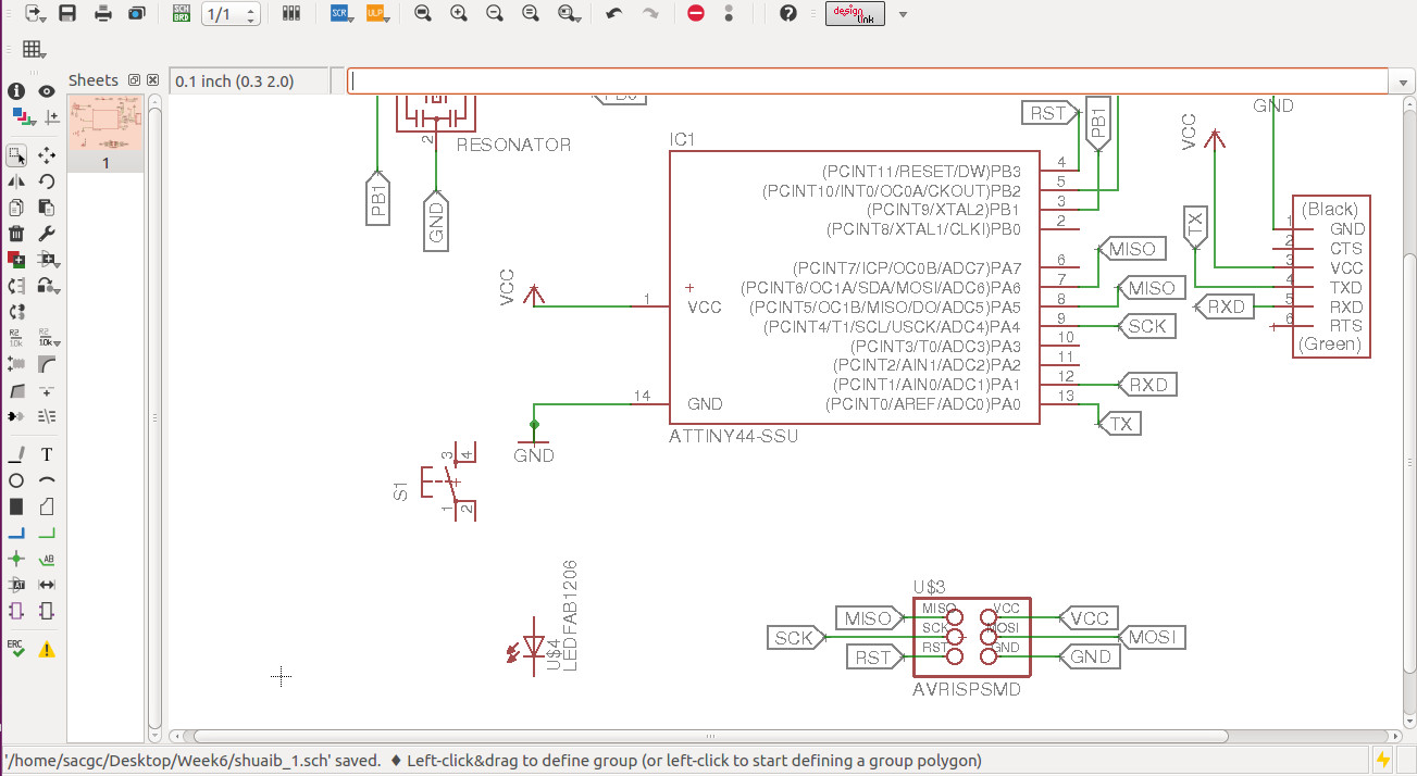
firs of all, I have started to redraw the circuit design provided by the fab-lab. In the beginning, it was difficult to redraw and select the option. But once the connection concept is established, it became easy to connect the components based on the names provided in the design. I have added 2 components in the design a switch and an LED. Below are the screen shots of adding net , labeling objects , renaming them and then connecting them to the assigned objects.
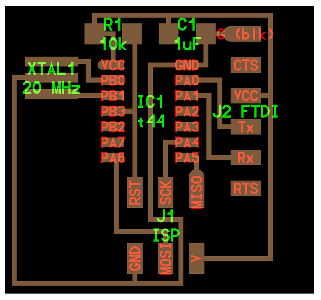
1) For the LED, I have added a resistor and connected it to the micro controller pin PA2 and the the LED in the other end. The LED is connected to both the resistor and the GND on the other end.
2) for the switch, I have connected the micro controller pin PA3 to the switch-4 and GND on the other end. Then I have to rearranged the components in a board format as shown in the picture below. I was trying to reduce the size of the board by keeping the components close to each others and then run the “Autorouter” option. The results kept showing a 90% to 95% every time I run the Auto-Router to connect my components.
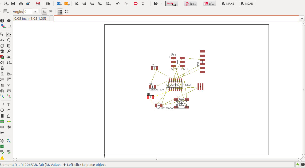
I kept using the command ripup: to move the components around and avoid any overlapping in the tracing channels. The difficult part is to find the connection and try to avoid it by the “ripup:” command every time and then to rerun. After more than 10 runs, I have finally succeeded in a 100% run.
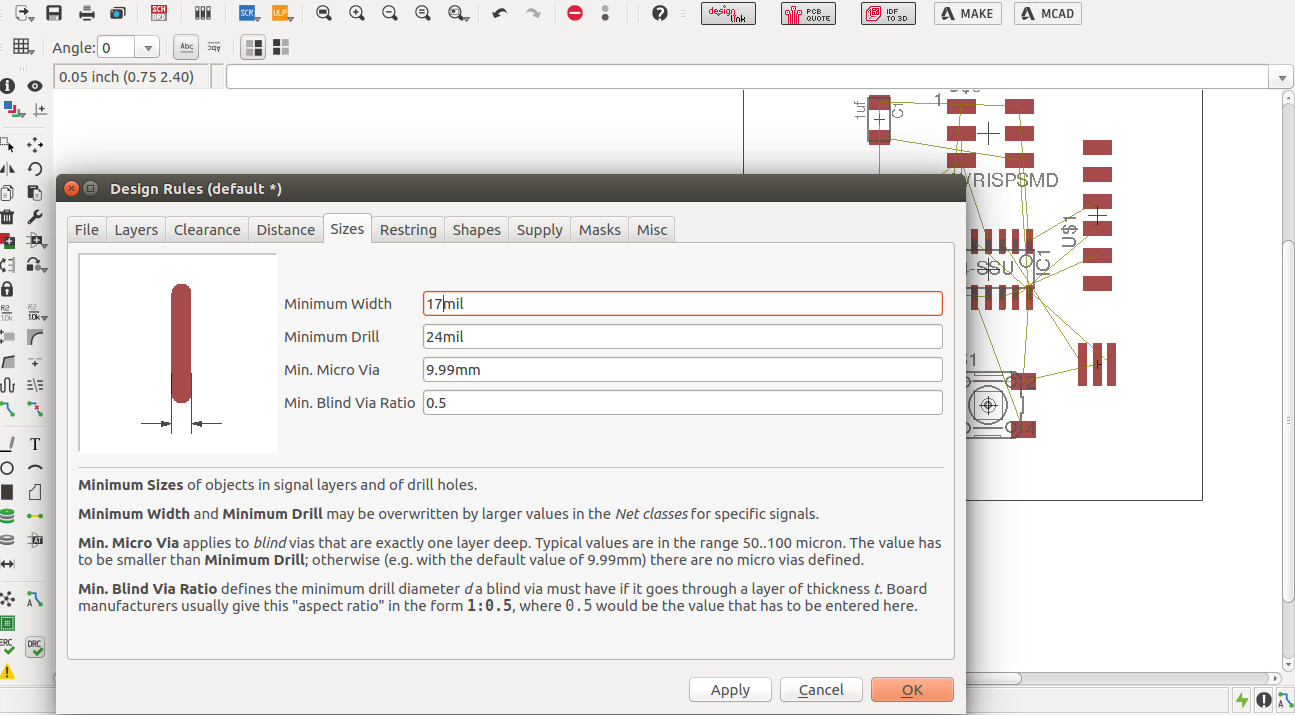
the tough part begins here, I had to increase the width size of the tracing channel in the design rule option to 17mm, minimum drill size is 24mm, and thats where the difficulties started. Up to this point, I re ran the Autoroute option (after the resizing the channels) more than 10 times and never got this part to reach 100%. I tried shifting and rotting the components to avoid any conflict in the wire channels, and it didnt worked. below are the step by step images of my first board design run which was a failure
This first step shows the design that was selected from the fab lab website
This is the first part in selecting the fab lab file uploaded from the fab lab website to use the components required only
here i have selected the design required by the fab lab to copy. please note that this design is for learning purposes and will add an LED and switch later on as required by the fab lab
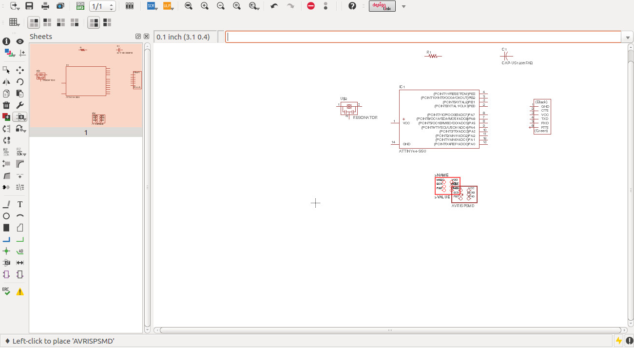
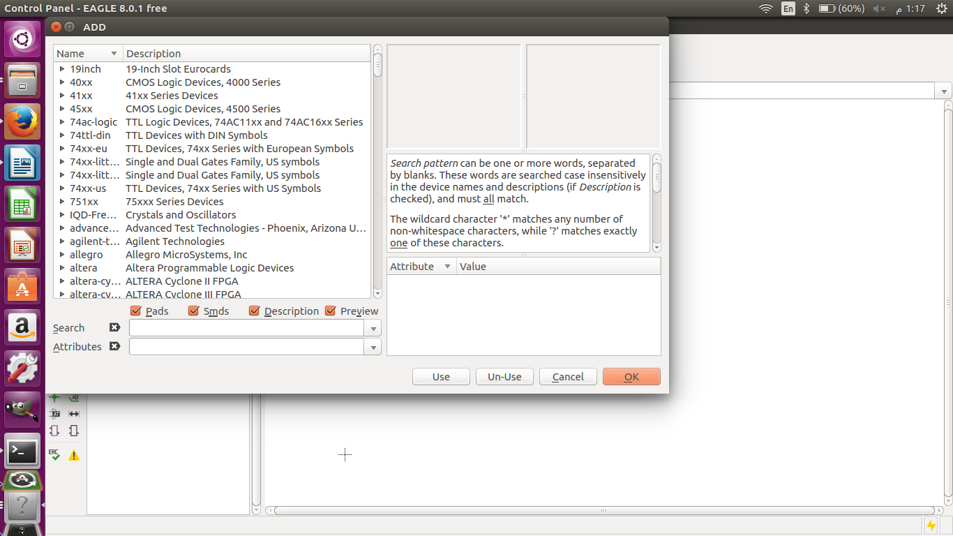
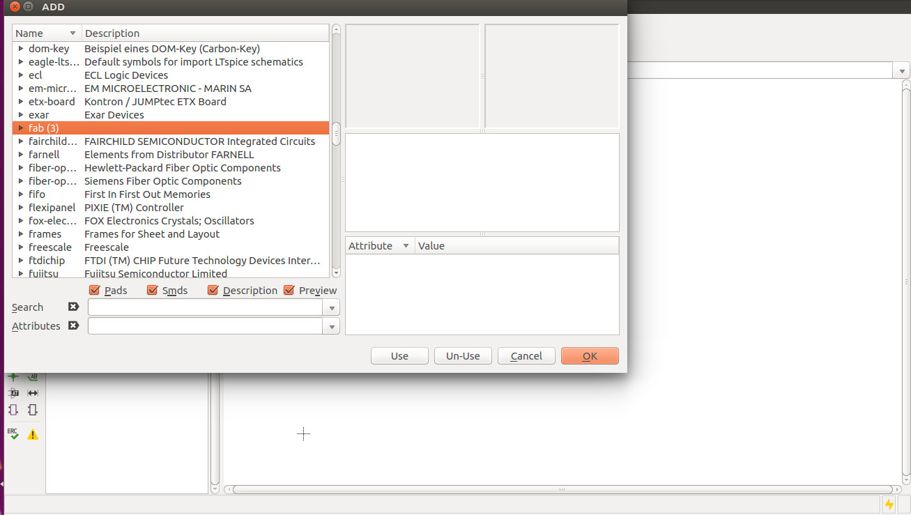
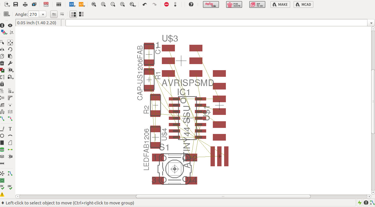
this pic shows all the 6 parts selected nd distributed on the bord as per the circuit design. i have used the option ADD and then serched for each component as shown in the circuit design and placed it in the board
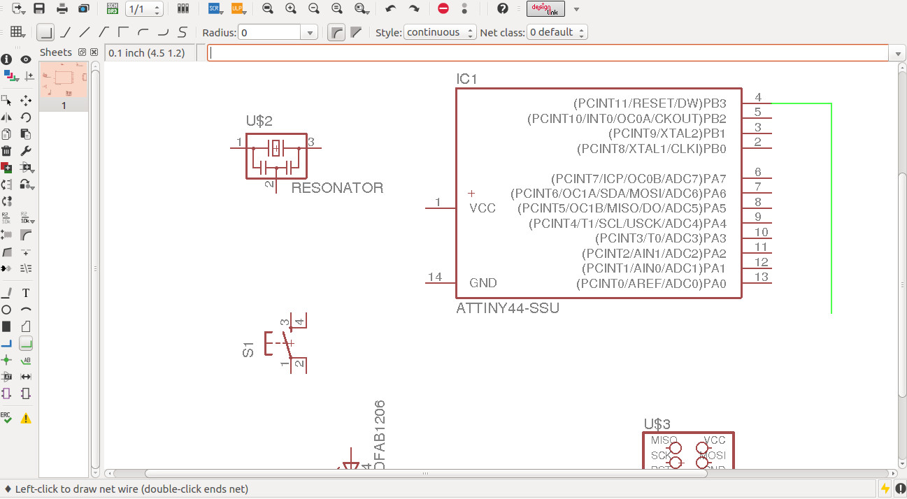
in this step i lerned how to use the NET option to connect components as one way to do it
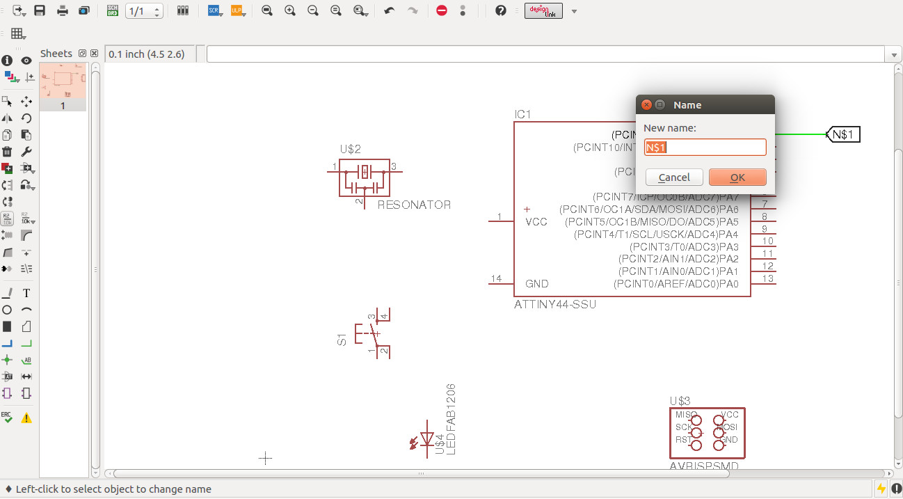
here is the label then the rename option to connect the components
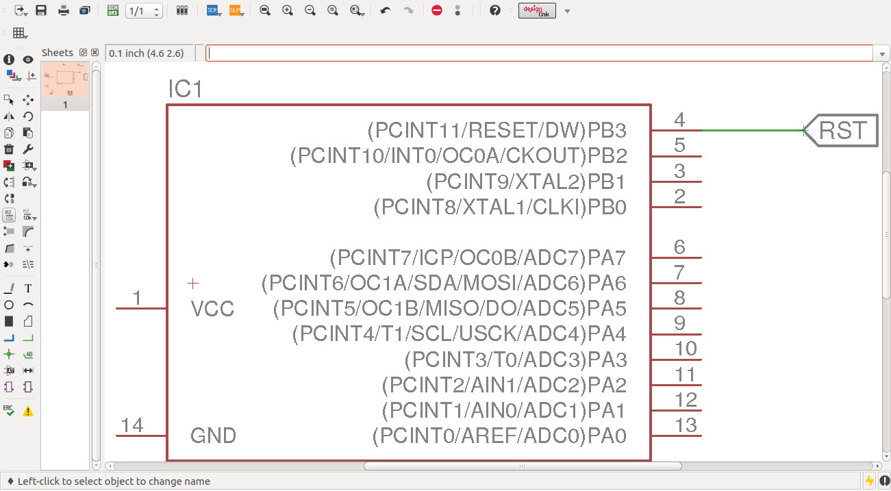
here i have renamed the component to RST to connect it later to the RST below
from this step onward, i have repeated the same method as specified above , the net , the alabel, the name. i have repeated those steps for each component and made sure it is connected to other components such as GND or VCC ... etc as required in the circuit design
here is just a repeat of the steps above and applied it to all components. this is still the easy part
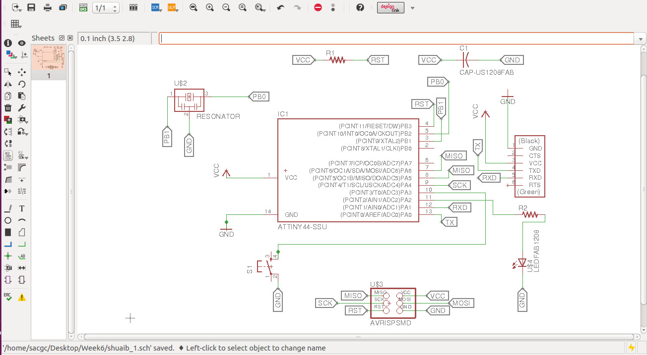
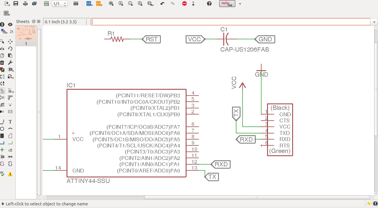
here is the complete circuit design as required by the fab lab. please note that i have added a resistor R2 on the right part of the board and connected it to the LED to control the circuit flow. and connected the other end of the resistor to the main control board PA2. for the LED, it was connected to the resistor and the Ground GND as shown in the picture.
The same concept was repeated to the switch i added on the bottom left of the board and connected it to the main control PA3
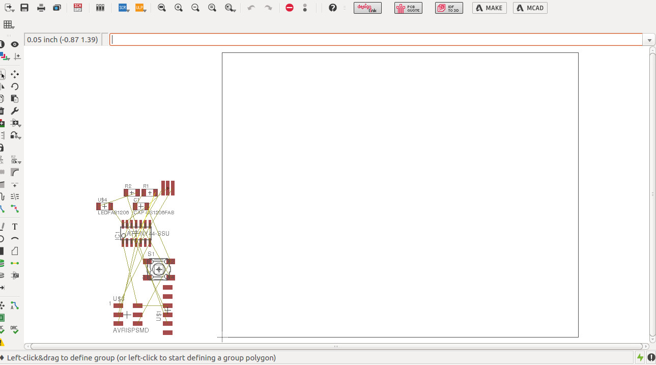
THIS is the TOUGH Part of the circuit design. i have converted the file into a board brd format in order to organize the tracing channel and make it ready for milling just like the previous week. so i selected all the components and placed them into the board to start the rerout runs
This picture shows the steps of placing them into the bord prior the rerout run
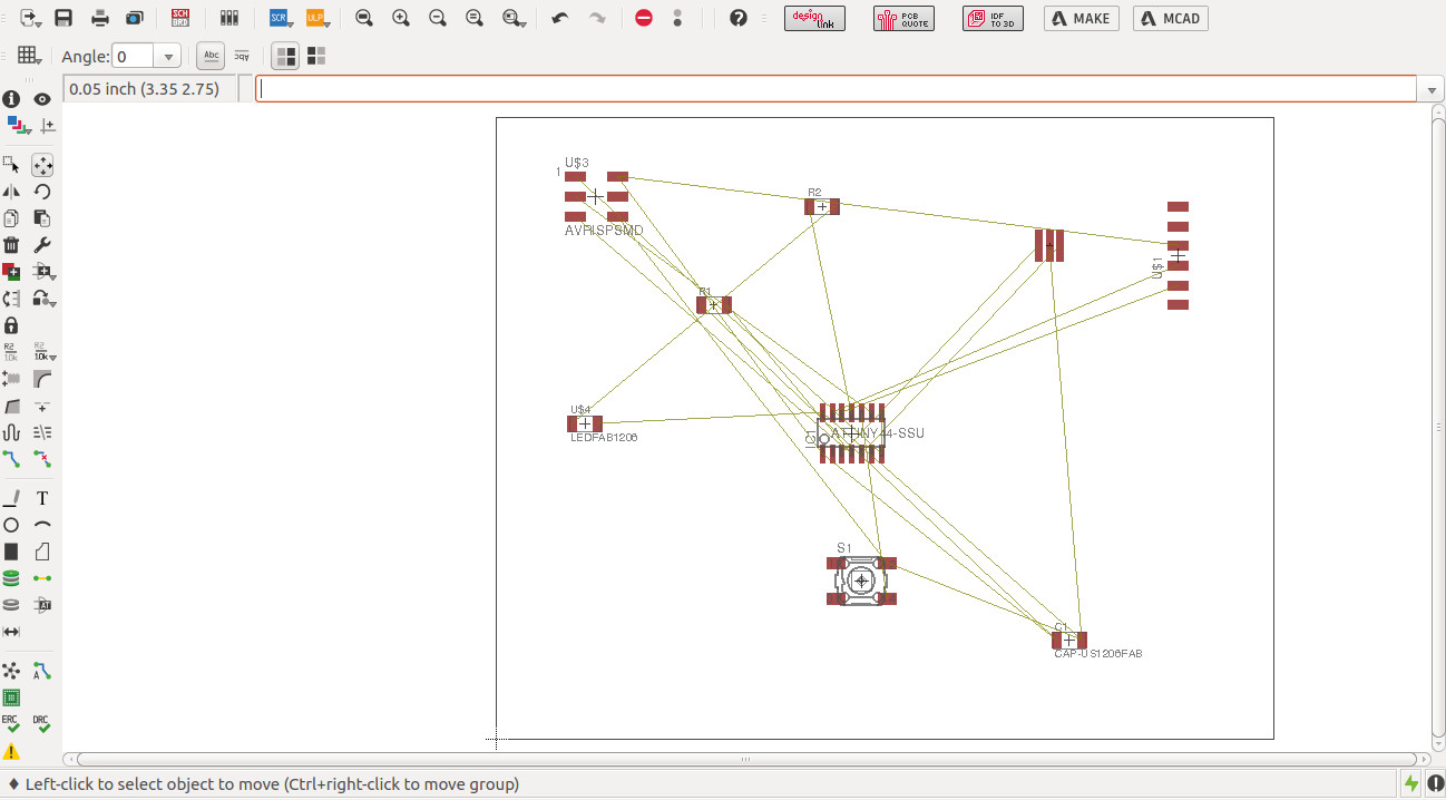
the full components and cicuit design is placed into the board
Here I was trying to reduce the space between the components in order to reduce the size of the board
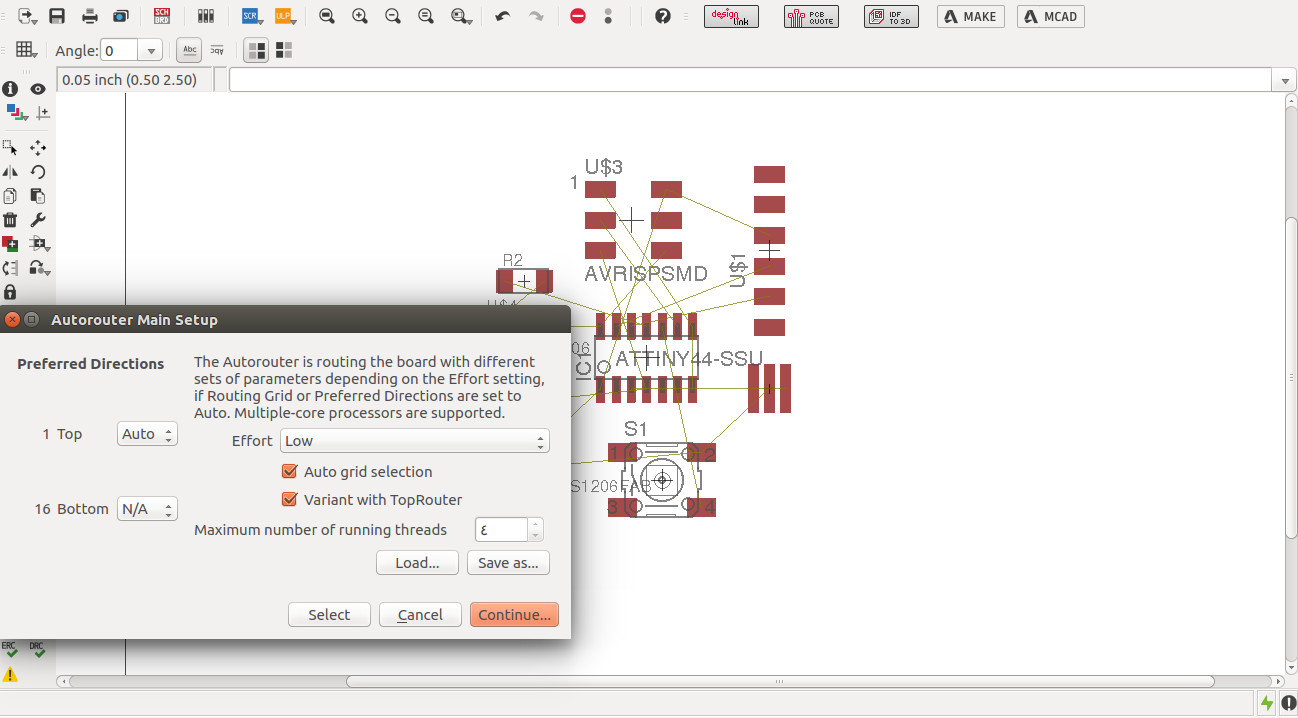
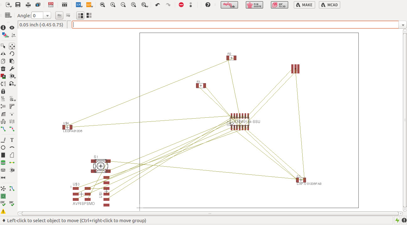
The Autorouter Run option which was repeated more than 10 times
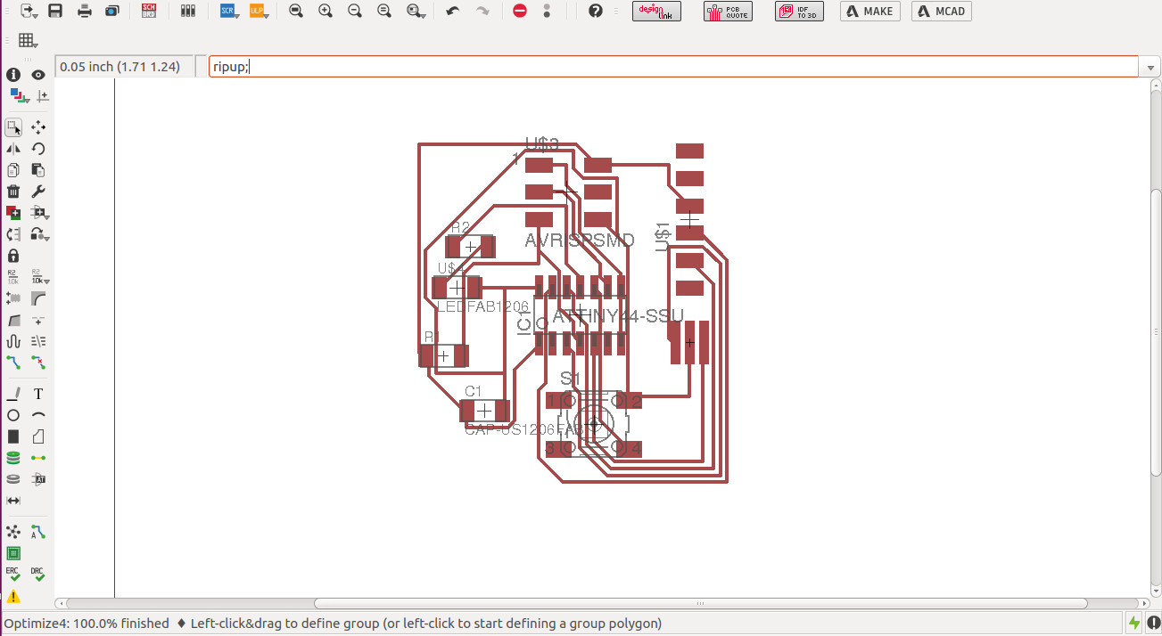
this run was 95.2% clear
here i had to use the ripup option to shift , chnge and rotate some crossed components to reach 100% clearance in the circuit channel
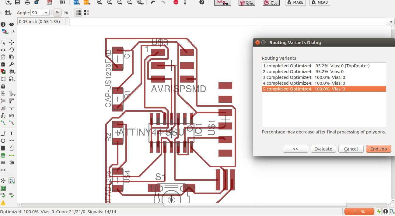
Here was at least the 10th run until i reached the 100% clearance on the circuit design but didnt apply the tracing channel width increase to 17mm which has messed up all the route runs again.
after this step, i re applied the rerout option for more than an houre and the best percentage of circuit clearance i recieved was 95.2% and went down to below 80%.
after this point i really decleared failure in this design and will have to redesign the circuit in away that would make all the route clear at the run.
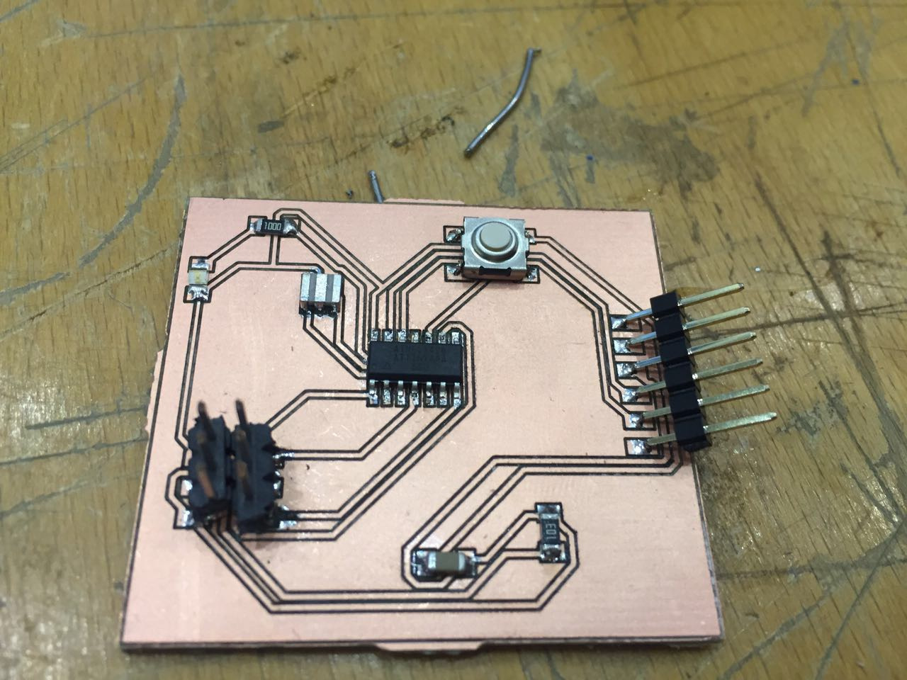
NOTE: The 3rd run, I have completed the design and it was 100%. the CBP Board was milled in the same previews process and the components were soldered. after completing the soldering, i found out that i have miss spelled one of the connections from MISO to MOSO. so i had to fix the connection in the circuit design, and reprinted the PCB Board for a third run
2 - Board Milling Process
I have followed the same process learned in week-4 in the milling and the soldering steps. So i had to convert the board file through the CAM Command in eagle cad to SCH in order to mill it in the milling machine. one of the difficulties here was the lack of pins provided in Fab lab Kuwait which has delayed the production for another week.
Anyhow, in the milling machine, the X and Y axis was set perfectly, but the Z depth was tough especially when the milling machine surface was uneven due to over use. to fix this issue, i had to remove the the sheet and make sure it is flat on the machine and had to take a risk every time i select a require Z value or a depth.
after assuring that the XYZ axis are perfectly set through the test run option, i selected the boarder area and sent the command to mill the PCB Board
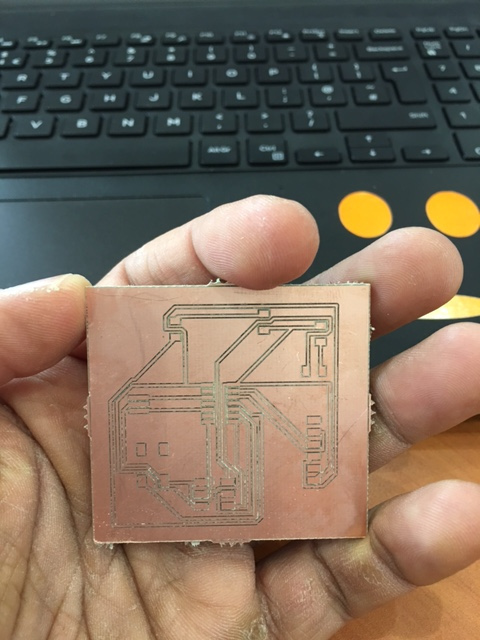
NOTE: here is the last milled attempt ready to be soldered. below is a link used in week-4 of documenting the milling process. the same process was used in this week as well
and here is the BRD file used My File
and here is the SCH file used My File
3 - Soldering Process
with all the issues i faced in the soldering process, i had to read off the Internet to find out the best way to do it. i found a general article that covers all aspect from selecting the best equipment to solder, to the safety during the soldering, and ends with the best was to do it and how to avoid short circuits at the end. it is a very useful article that i shared with some of the colleagues. here it is
www.inlandcraft.com/howto/pdf/htsold.pdf .here are some of the useful tips quoted from the artice above that helped me during the soldering:
1) Solders are easy to use and relatively inexpensive.
2) Low energy is required to solder.
3) Properly soldered joints are highly reliable.
4) Solder joints are easy to rework or repair..
5) Experienced craft persons can exercise a high degree of control over the soldering process.
9) Solder joints age very well. They can last for years, decades and centuries.
Difficulties and Lesson Learned
the cleaner and neater the circuit design is in the beginning stages of the design, the easier the reroute option would be. so I had to redesign the circuit from scratch again. due to the following mistakes:
1) GND connection was at one end only
2) MISO connection was miss spelled on the other end of the connection as MOSI
3) an assembling mistake occurred during the circuit check