WEEK-4 : Electronics Design
The 4th assignment in the Fab Lab was to do the following and report every step taken during the process.
Learning outcome
1) Describe the process of milling, stuffing, De-bugging and programming
2) Demonstrate correct work flows and identify areas for improvement if required
Have you:
1) Shown how you made and programmed the board
2) Explained any problems and how you fixed them
3) Included a ‘hero shot’ of your board
1) Design Process
Started week-4 by short lecture by the local instructor as a refresher about the circuits and how it connects and what are the input and outputs . Then I downloaded the eagle auto-desk software from www.autodesk.com/products/eagle .
the dsign components used are the followig:
- LEDFAB1206
- S1
- ATTINY 44
- AVRISPSMD
- Capacitor
- 10K Resistor
Here is the board file used in designing , milling and soldering the circuit My File
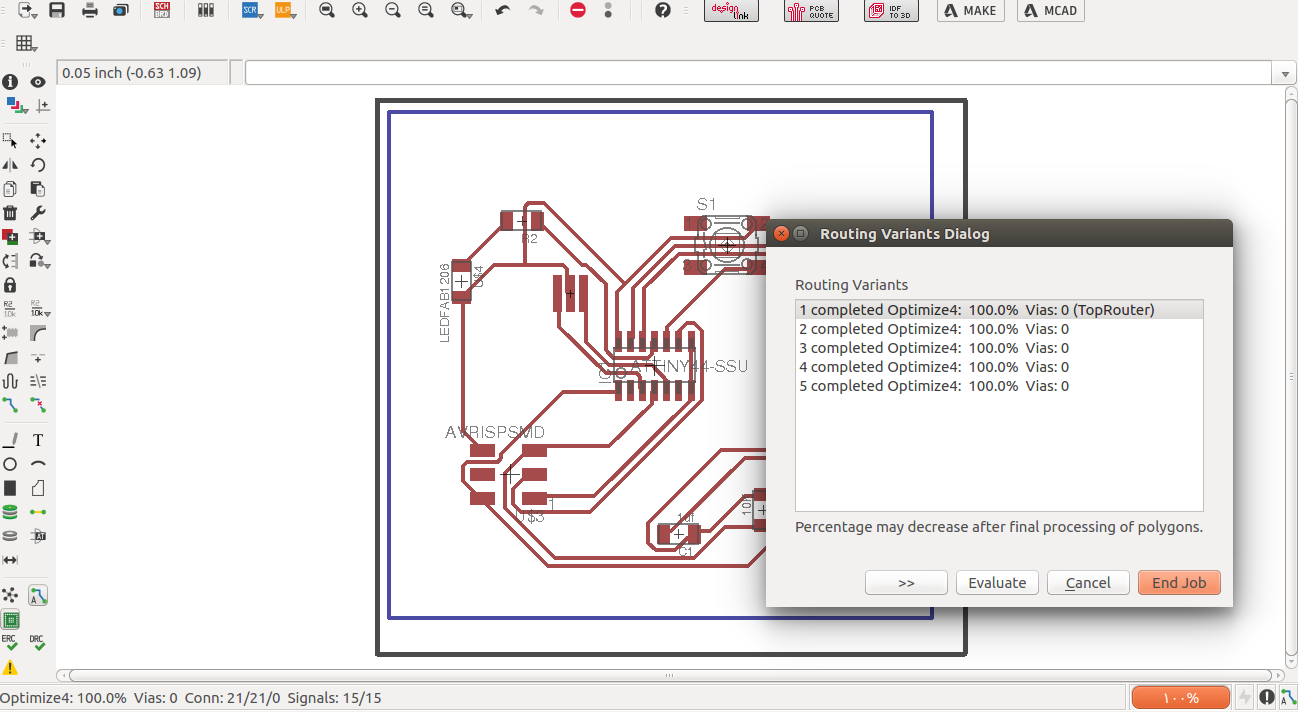
I started the design process by opening a new circuit plan in the eagle auto desk and then downloading an existing plan from the library option following the ISP fablab assessment requirement. and ten selected all the required components for the circuit as per the design in the picture below. the main focus in this step is to design the circuit at 100% rerouting and send it to the milling machine.
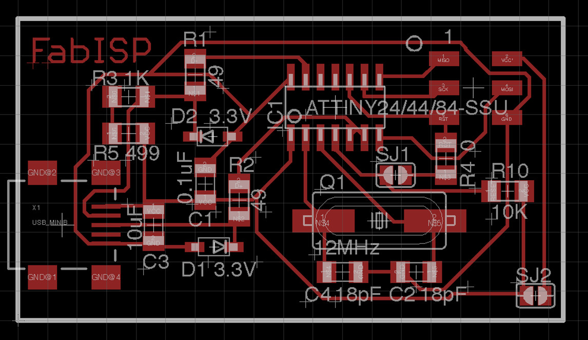
so below is the schematic heroshot of the circuit i designed:
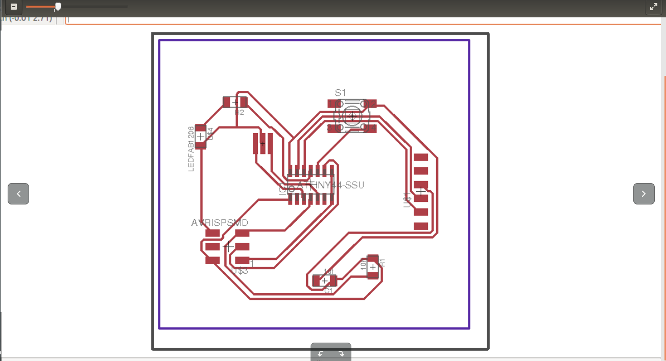
the main issue faced in the design of the circuit is the rerouting option. finding the best route for the circuit was not as easy as expected. the picture below shows a 100% rerouting.. I had to learn how to check all the tracing in the circuit and make sure they don't interfere with each other especially after the milling. this step was not necessary at this stage, but learning it now will help alot in the upcoming weeks. I had also to check the thickness of the tracing as well and how close he components are from each other.
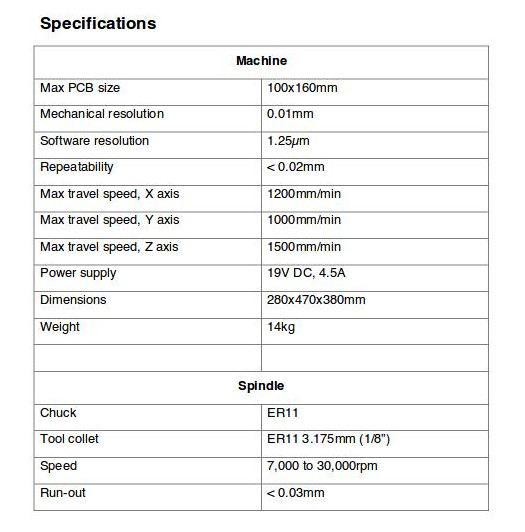
About CirQoid milling machine
Here is a PDF user manual for the CirQoid milling machine we used that i wanted to share with everyone. It includes all the details in pictures abou the machine specification, how to use it, how to fix XYZ axis, emergency button, fixing PCB, fixing any add ons any many more details that helped personally in addition to the local instructors orientation given in that day CLICK HERE.

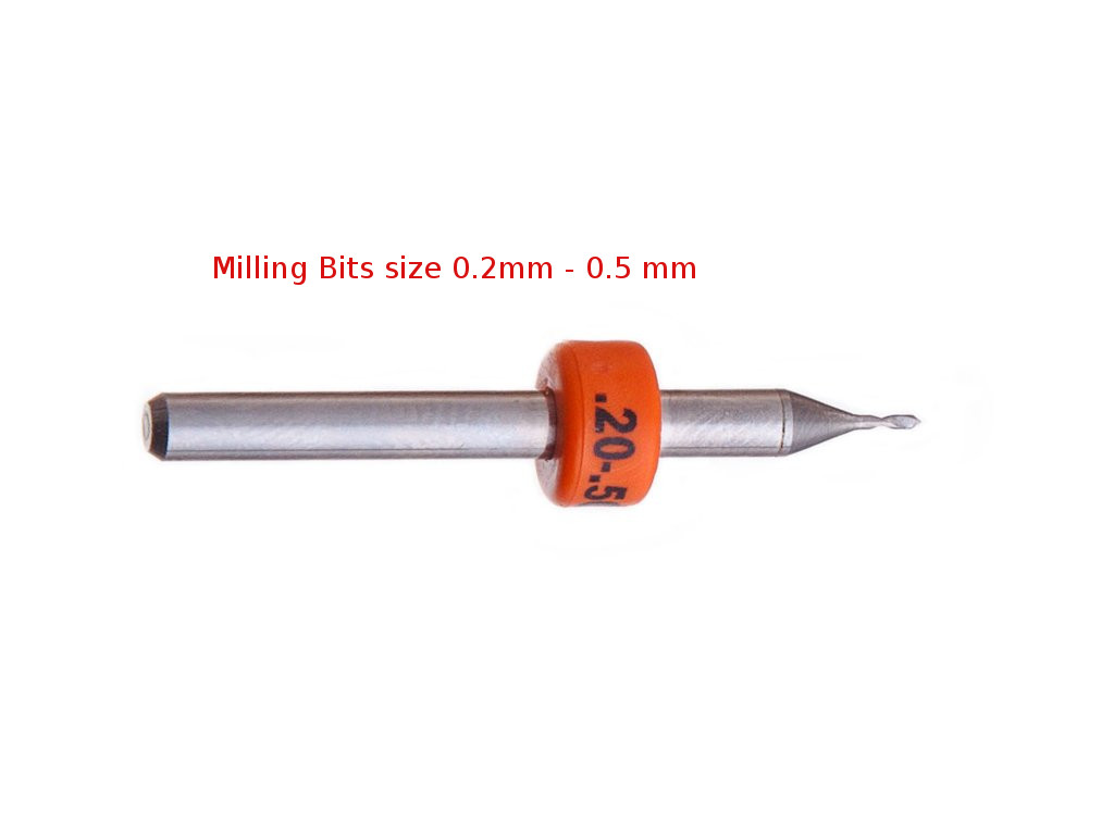
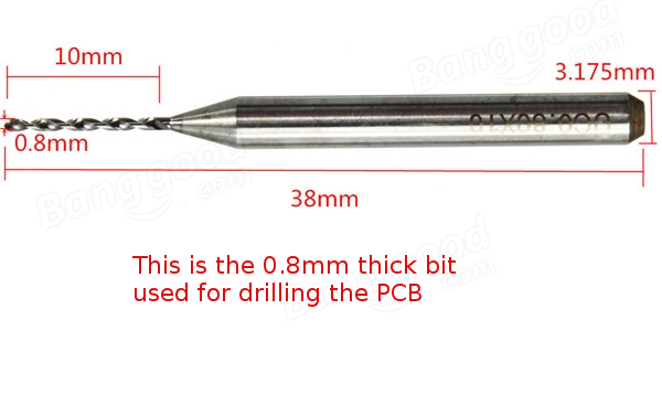
About Drilling and Milling Bits
in the achine above, a papckage of milling and drilling bits was available and it varies in thickness and sizes depends on the requirement of the milling. In my case I was using the the 0.2-0.5 mm milling bits and a 0.8mm for he drilling bits as seen in the picture below:
2) Milling Process
I sent the design file to the CirQwizard milling machine to print the copper board as per the required circuit design. The thickness was the most important element in the editing of the machine in order to assure a good milling of the board. Setting the X, Y and Z axis on the machine and testing the depth and each side of the board prior milling the copper board. After assuring that all coordinates are within the board dimensions,I fixed the Bit into the machine and then sent it to mill.
as shown in the video below, the copper board must be placed evenly on the machine and the right bit should be placed for the right task. After milling the circuit itself, the software will ask to drill the outline around the circuit to assure that the removal of the circuit is smooth as well. See the picture below and the video as well to explain the process that was taken.
3) Components Soldering Process
the equipment used in the soldering is the fowlloing
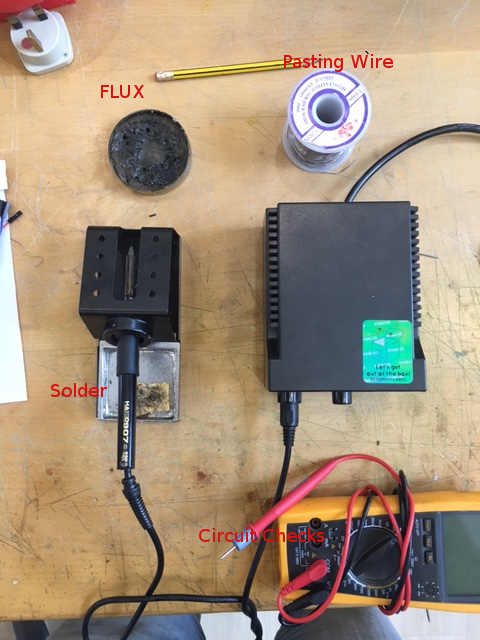
After milling the copper board, I transfered to the soldering station which includes the soldering machines, circuit-shorts check ups and finding all the required components of the circuit. the most difficult part in this process was to assure that the soldering was done properly.
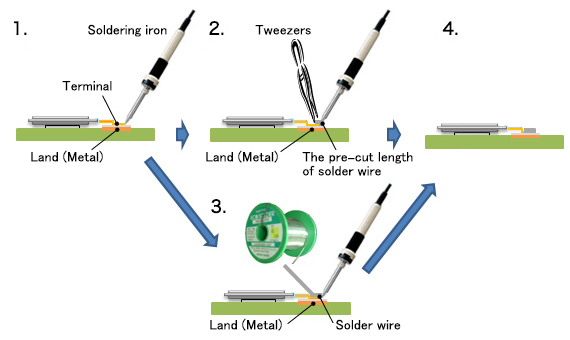
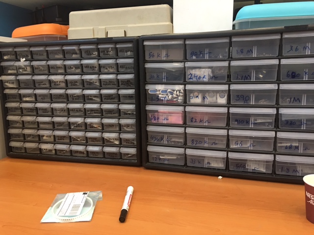
so i really suggest to practice the soldering away from you currently milled board and get used to it. Below is a picture of all the available components in our lab. so we had to look for each component required for each circuit, list them and then safely place them on a piece of paper in order to assure that the required component and properly selected.
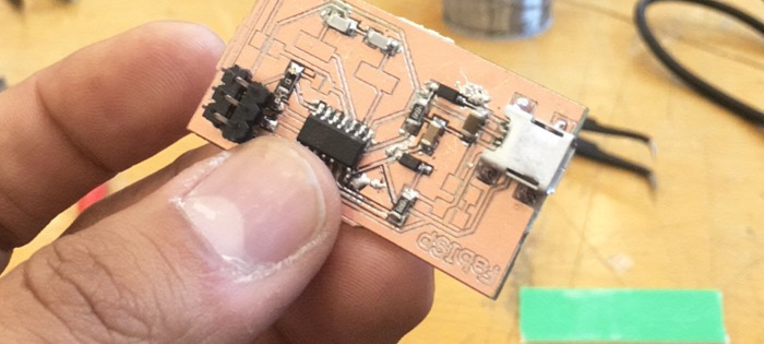
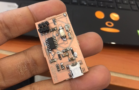
I had to solder each component and check its short-circuits if it beeps or not. Then i had to remove and connect some of the components as I kept failing in connecting it. i repeated all the soldering steps for each component to clear it from any short-circuit if any. The pictures below show some of the progress I have made in finalizing the board. luckily, i succeeded in having a perfectly running circuit and short free as well.
4) Programming Process
After finalizing the board with all required components, I have started the programing process of the micro controller in the board by downloading the files from fablab website by downloading the following software Crosspack for AVR. HERE.
Then I downloaded the FabISP Firmware My File. . Then i connected the board to a 3 by 2 connector and started the programing process. below is the final step captured as a screen shot.
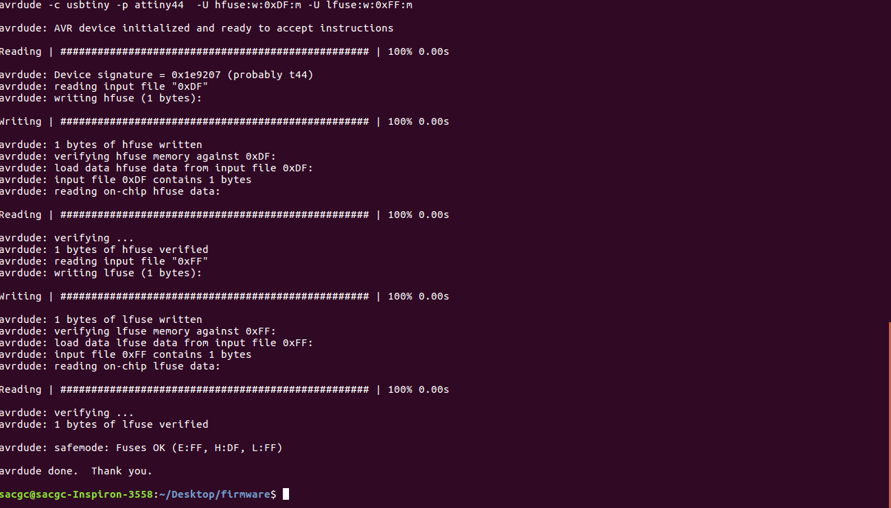
the pic above of the final programming. The code used in the terminal was the following:
1) Sudo make fuse
then
2) Sudo make program