06. Electronics Design
Assignments
- Redesign echo hello-world board in any PCB design software and interface a button and LED to ATiny44.
- Check the design rules, make it, and test it
Learning PCB design Software - Eagle
What is Eagle
EAGLE stands for Easily Applicable Graphical Layout Editor (German: Einfach Anzuwendender Grafischer Layout-Editor) and is developed by CadSoft Computer GmbH. Cadsoft Computer GmbH was acquired by Autodesk Inc. in 2016.
EAGLE contains a schematic editor, for designing circuit diagrams. Parts can be placed on many sheets and connected together through ports.
The PCB layout editor allows back annotation to the schematic and auto-routing to automatically connect traces based on the connections defined in the schematic.
Download, Install, Run
EAGLE is available on Cadsoft’s (the developer company) download page. EAGLE installs just like any old program, it’ll self extract and then present you with a series of dialogs to configure the installation.
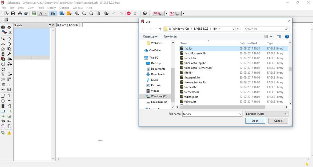
Adding library
After download and installation of Eagle, I realized that I need a components library to find the components we need for our design. So, I downloaded the fab.lbr from here. Then I saved the fab.lbr to the right libraries file folder (In my case: C:\EAGLE 8.0.2\lbr) & did settings in Eagle to use the fab library.
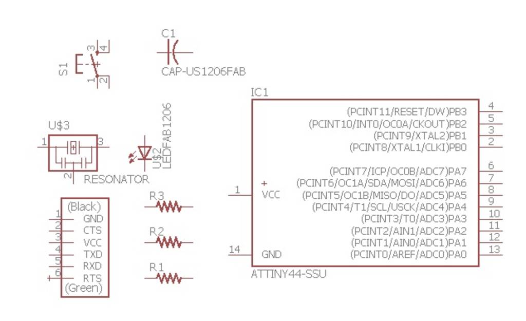
Adding components
Then I started making the scehmatic of echo hello-world board. I prepared the list of components needed for making echo hello-world board as follows :
-
Electronic Components for Hello world board from Fab Library
- ATTINY44-SSU x 1 - Microcontroller
- LEDFAB1206 x 1 - LED
- CAP-US1206FAB x 1 - Capacitor
- RES-US1206FAB / 100k x 1 - Resistor
- RES-US1206FAB / 10K x 2 - Resistor
- FTDI-SMD-HEADER / 1X06SMD x 1 - FTDI header
- 6MM_SWITCH x 1 - Switch
- RESONATOR 20 M x 1 - Crystal oscillator
- AVRISPSMD / 2X03SMD x 1 - Haeder 2X3
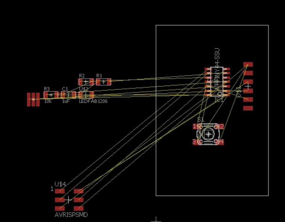
I added all the components in schematic sheet by using add menu & selecting required components from FAB library.
Connecting the components
- There are two was to connect components in a schematic:
- You can connect the components with a wire (also called a "net" in Eagle). This may make connections obvious at first, but can get really messy quickly as nets cross over each other.
- You can also name the nets attached to components that need to be connected by naming them with the same name. See example schematic above. Eagle will ask you if you want them to be connected. (Say yes!). After you name the component - label it so the name appears in the diagram.
I used both methods for connecting the components.I used label command to show the name of each net to make the schematic readable.
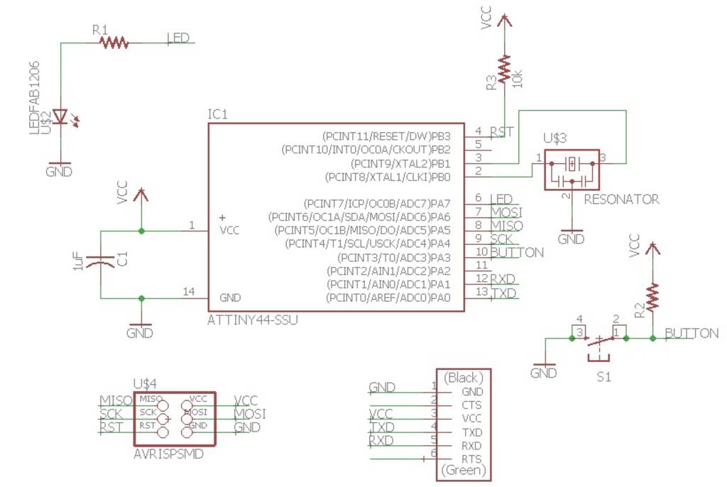
Adding LED & Button
I added a button and an LED to the design.
When adding the LED, I made sure to put it in series with a current-limiting resistor. To estimate the resistance required, I considered using a red LED, which has a voltage drop of about 1.8 volts. With a desired current of 5 mA (approx) through the LED, a (5 V - 1.8 V)/(5 mA) = 640 Ohm resistor is required. So, I decided to use 499 ohm resistor (because 460 ohm resistor was not available.
When adding the button, I decided to use a pull-up resistor configuration. Essentially, the microcontroller’sinput should always be driven high or low, and using a pull-up or pull-down resistor with the button is a way to achieve that. I chose to use a 10k Ohm resistor. To understand the basics of pull up or pull down resistor, click here.
I decided to connect LED to PA7 & button to PA3.
Here is the final schematic with the button and LED added:
Routing teh traces on the board
Then I swiched to board layout view. The components I had added were jumbled up in a corner with yellow unrouted traces attached. I used move command to arrange the components at proper place.
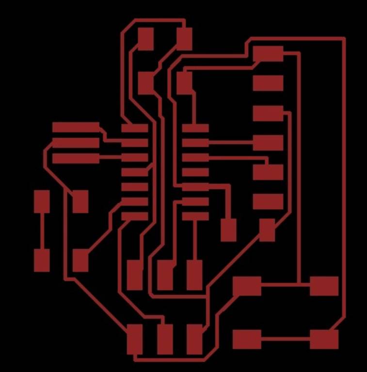
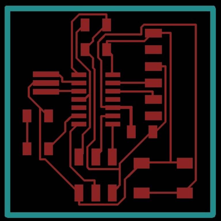
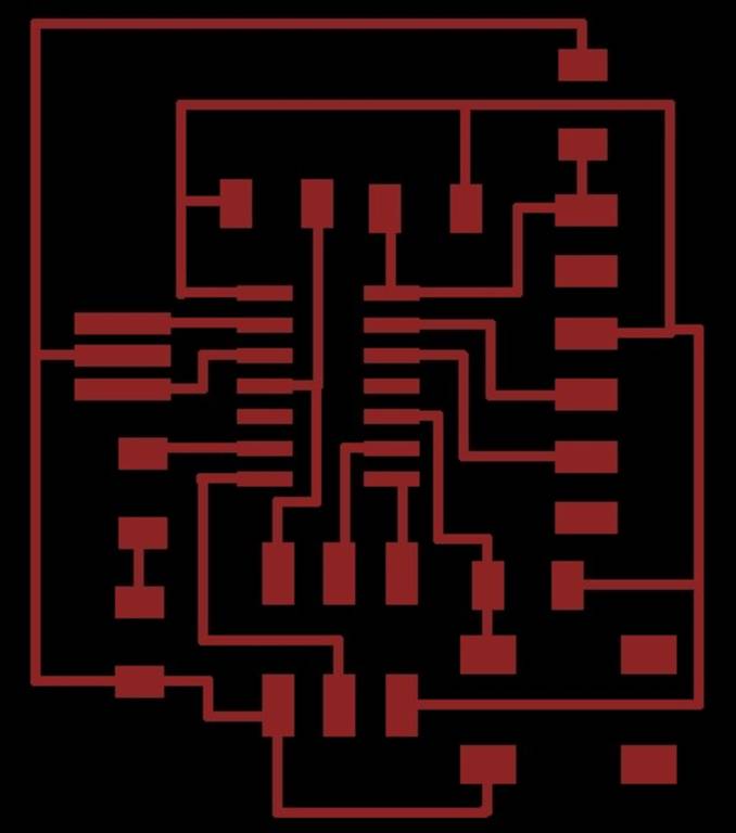
For routing, I used auto route command. After few trials, I managed to generate layout as shown below:
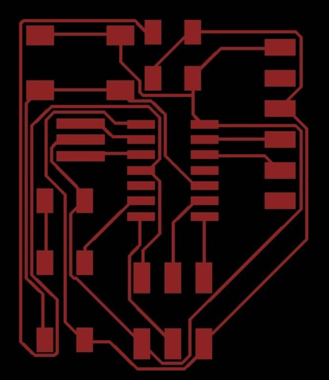
Exporting board layout to be used with milling machine
Eagle can export PNG images of PCBs. I just needed to disable all the other layers but Top layer in View > Layer Settings, so that I could get a clean image.
I exported an image at 1000 dpi. Here is the final result:
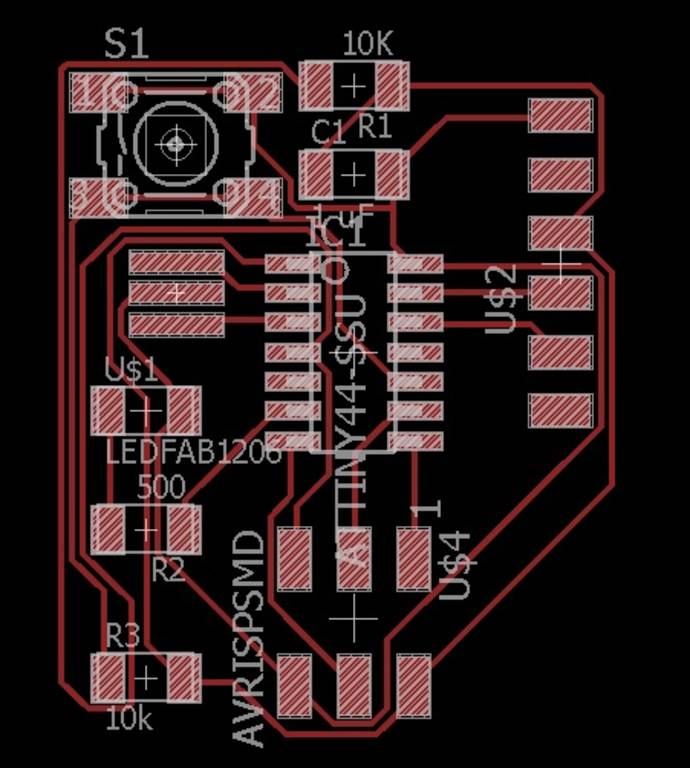
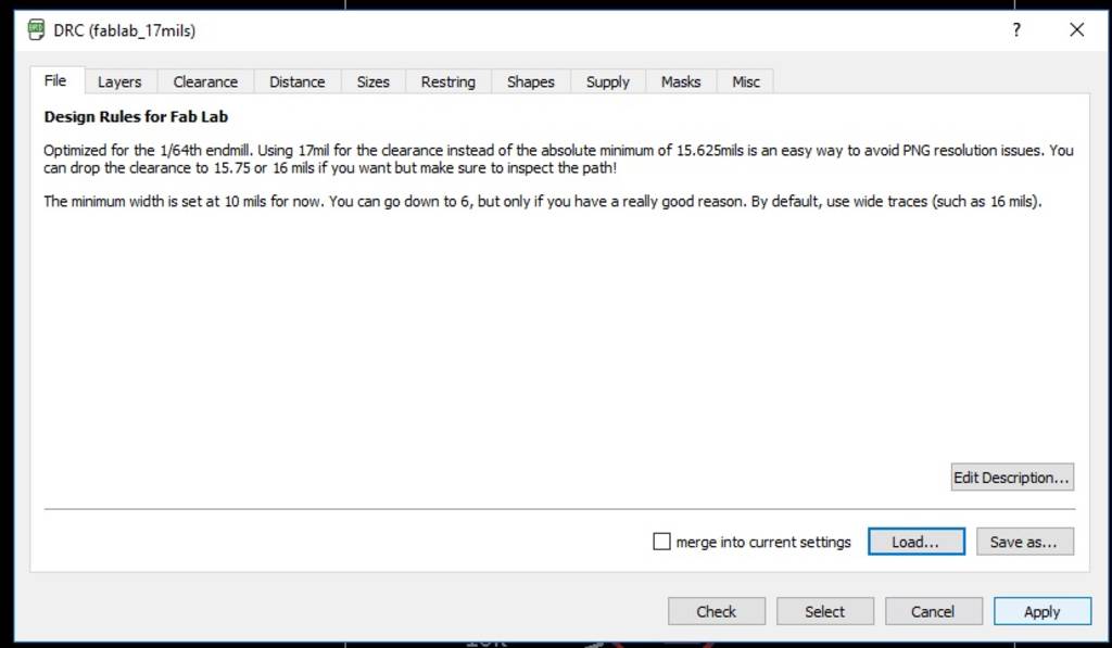
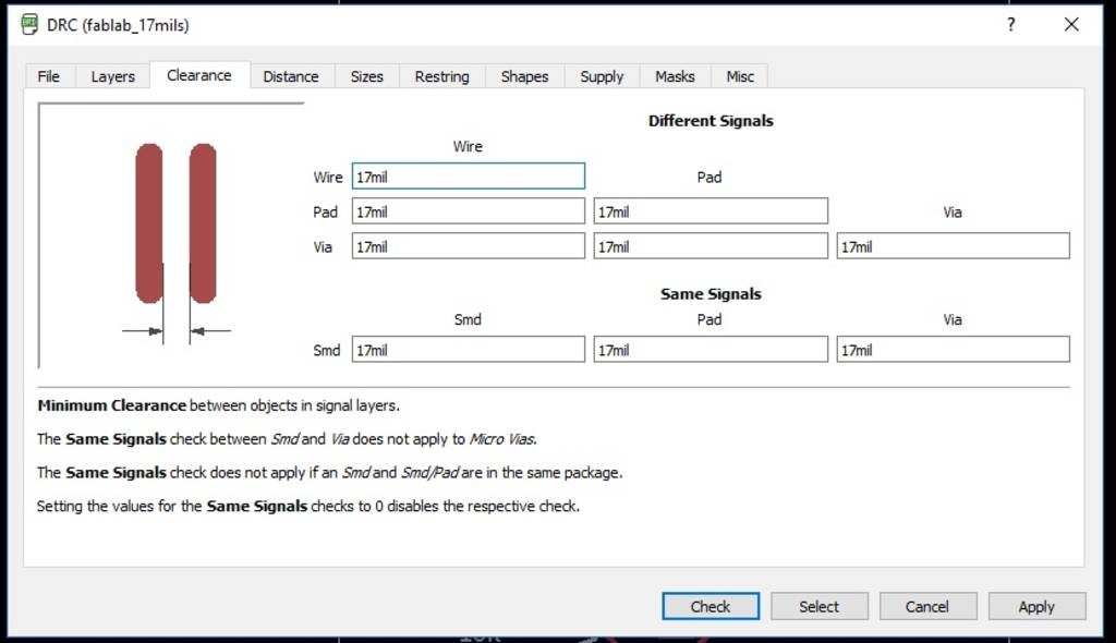
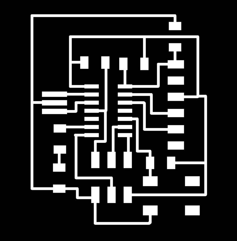
Then I milled this image on copper clad by using the method we learnt in Week 4. But the milling failed because distance between any two tracks was too less to mill it using 1/64 inch endmill. Then I went through the websites of previous FAB LAB students to find the solution of this problem. And, I came to know that for proper milling I should use the proper design rules.
we used 1/64 inch endmill. 1/64 = 15.625 mils. we should use a clearance of AT LEAST 16 mils. 17 or 18 is probably safer. Hencr, I downloaded 17 mils DRU file fablab_17mils.dru
Then I used this dru file to set the design rules for current project.
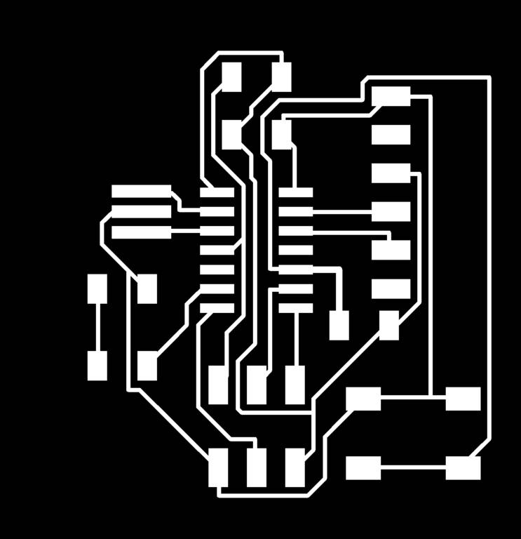
Then I repeated the steps of auto-routing & exporting board layout as .jpg Image. Here is the final result.
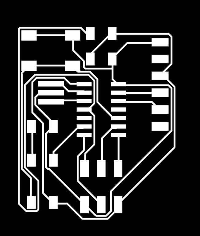
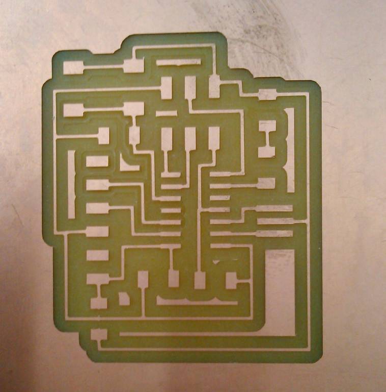
Creating board outline
I created the board outline in milling layer. I kept the width slightly greater than that of the copper layers. Then I make TOP layer OFF & exported the outline as .jpg image (monochrome).

Milling the PCB
During milling, I faced two problems -
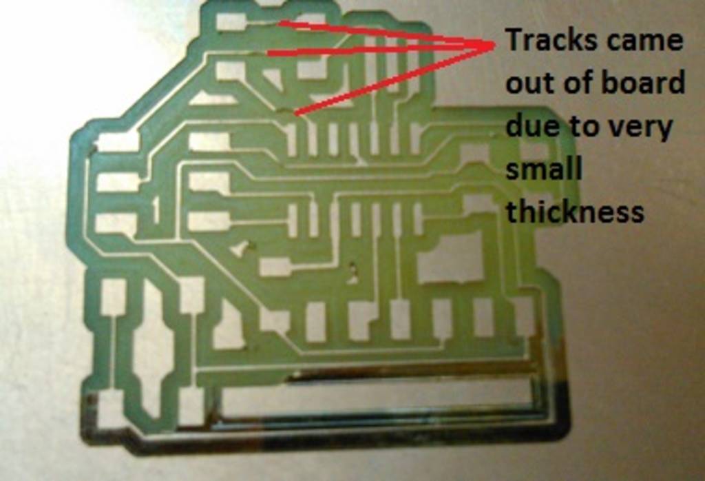
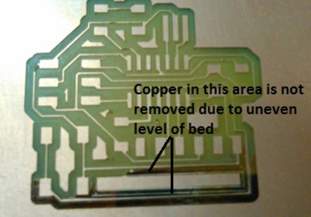
Solving the problem faced during milling
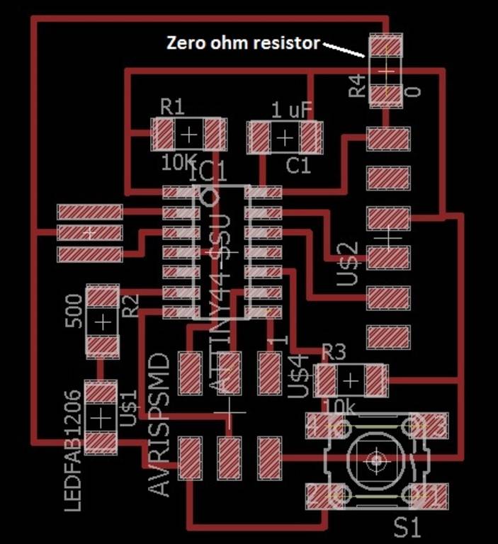
To solve first problem, I increased my track width in eagle to 0.4 mm (Initially it was 0.1mm). As track width increased, I faced problem in auto-routing. So, I decided to do manual routing. Also, I added one 0 ohm resistor in the circuit in order to complete the routing.
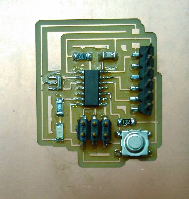
Finally, I milled the board using FAB Modules & MDX-40 milling machine & soldered the components. While milling the outline, I inverted the image in FAB Modules.
You can download project files here.
Design Rule File (17 mils)Hello_World_Schematic
Hello_World_board