WEEK 6 - Electronics Design
TASK:
* Redraw the echo hello-world board,
* Add (at least) a button and LED (with current-limiting resistor).
* Check the design rules, and make it.
* Create a Echo Hello-world Attiny 44 board following Eagle tutorial (fabacademy and Sparkfun).
* Test out different equivalent softwares.
* Milling
* Stuffing
Create Echo Hello-world board using Eagle
Software Downloads: Eagle
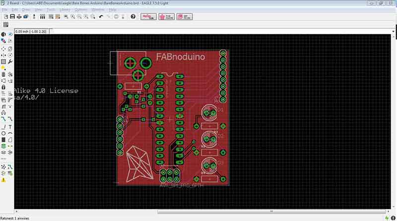
Download generated Eagle files: HelloTiny44_01.brd HelloTiny44_01.sch BareBonesArduino.brd BareBonesArduino.sch
1) Sparkfun Tutorial
Map of working process:
Download and install Eagle > Download Sparkfun Libraries zip file and insert in Eagle Directories > start Schemetic tutorial > continue with Board Layout tutorial.
Here are some of the critical steps:
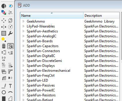
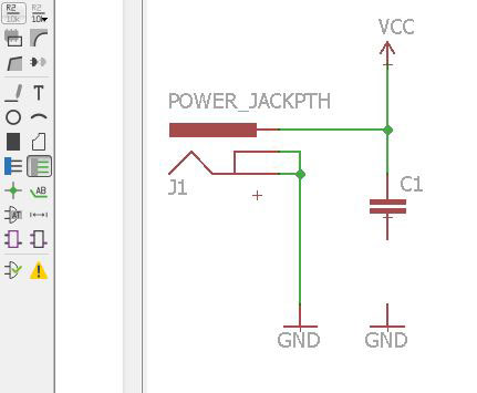
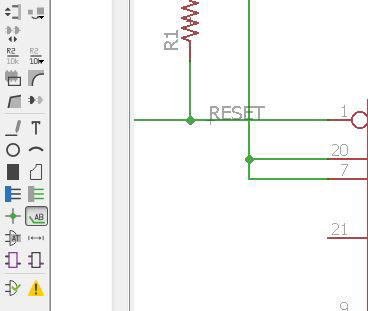
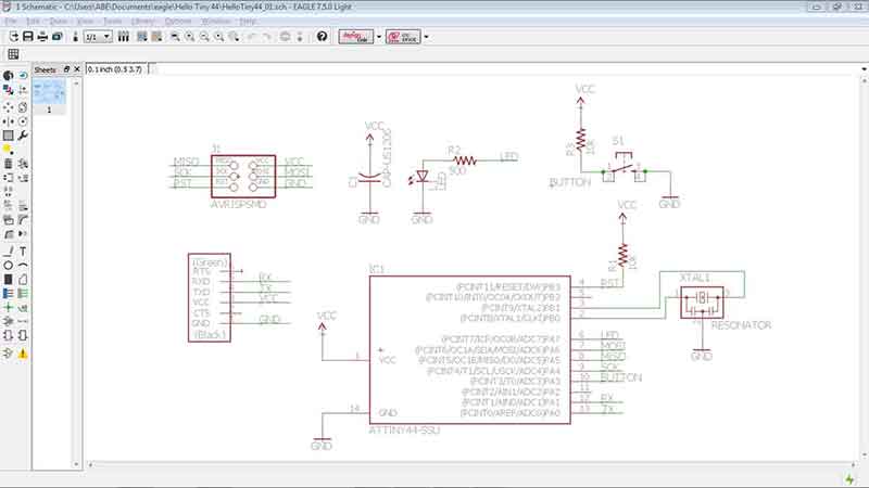
a) There are 2 main stages in creating a PCB design in Eagle. Firstly, a schemetic layout should be designed or put in place so that the software is able to generate a virtual board before proceeding to create or send data for milling. The schemetic layout is pretty much an assembly platform (refer to image below) where circuit components are placed together using either the default library or imported ones. Sparkfun has provided a customized library for purposes of making the tutorials easier. The step by step tutorial was indeed very easy to follow.
Critical steps for schematics design:
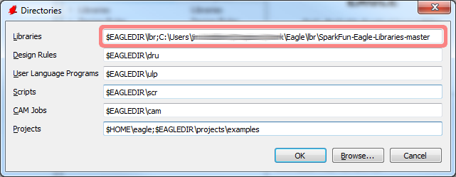
- Once installation of Eagle and Sparkfun libraries successfully installed, open up eagle and go to Control Panel> Options> Directories and update libraries. To update libraries, simply insert directory link seperated by a semi-colon (;).
- Next, create a new project by going to Control Panel> File> New Project. This will save the working file under the Eagle's root directory.
- Once the root directory is created, create a schematic working file by going to
Control Panel> File> New> Schematic. This will open up a new schematic window where
design can be developed. Remember to save the schematic file under the Project folder
located in the Eagle root directory.
-
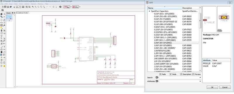
Add- Calls out a window of components to add on to schematic design.
-
Net- Connects components together with a green line.
-
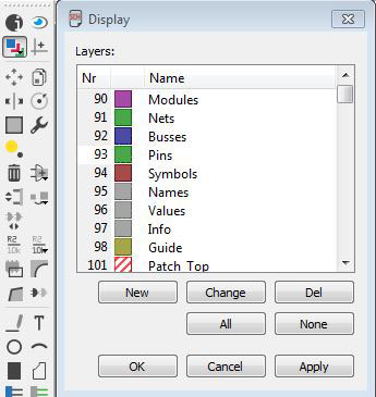
Layers- Controls layering of parts that can be turned on or off.
-
Move- Determins positonings of components.
-
Info- Provides information to each component inserted by clicking on component.
-
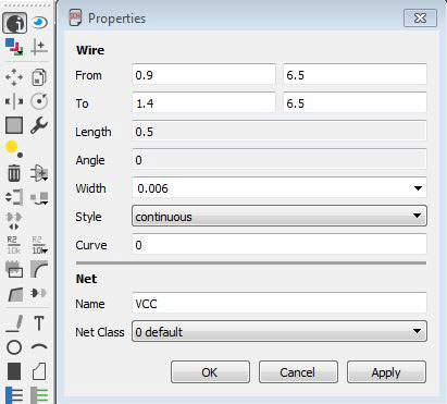
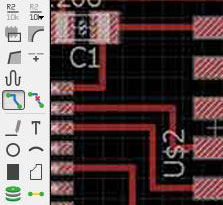
Naming and Labeling- These are 2 seperate functions. One button as an image with AB (labeling)
and the other has the word R2 (Naming) written over it. To name connections (green lines),
simply click the button with R2 first and select the green line to be modified and name the connection. Next,
click on the button with the word AB and click on the selected green line again. This will
create the desired name onto the green connection line.
-
ERC- Electrical Rule Check (ERC) ensures all errors in schematic design are presented to be rectified.
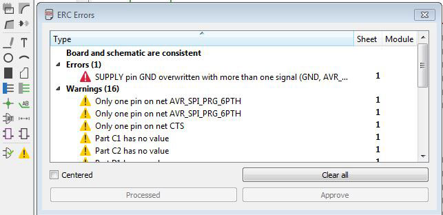
-
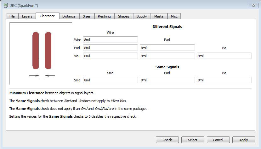
DRC- Design Rule Check (DRC) define rules for trace clearence and distances from components etc.
Settings will affect the board design and it's connectivity. Generally, this works hand-in-hand
with ERC so that as the connectivities were modified, errors were detected and design rules amended
to ensure good clearence between traces and components.
Generally, the settings for Wire and Pad ranges from 8 to 12 mil
and the rest of the settings were kept at 8 mil.
-
Once schematic design is completed, it should look like the image below.
From here, simply go to File> Switch to board.
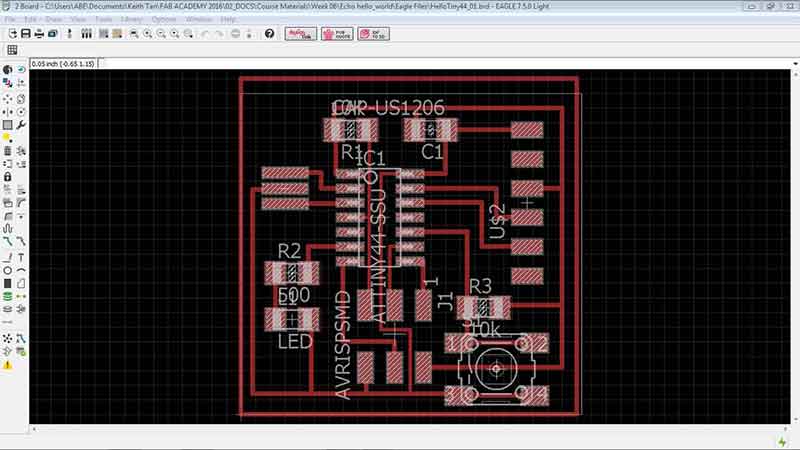
b) The second part of the Sparkfun tutorial is to generate the board and to do final touches. Once the board has been generated (as mentioned above), an alternate way to switch to board layout mode simply hold [alt] key on the keyboard and press [2]. To toggle back to Schematic layout, simply press [alt] [1]. The tutorial included instructions on creating silk screen designs on the board layout using the polygon tool as well as errors checking using the Design Rule Check function.
To complete the board design, here are some of the key steps:
Here are some of the commonly used functions during board design:
Sparkfun tutorial made the starting journey of PCB design a bliss and great fun. The only difficulty was the search for components in the library. Although the type-in search function was available, some of the components still requires some considerations before making the right selection.
2) Fab Academy Tutorial
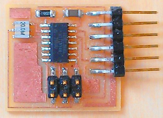
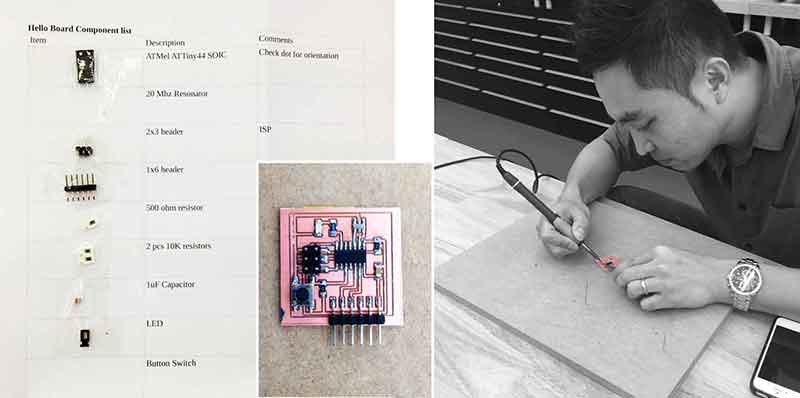
As part of the assignment, a Pushbutton Switch and an LED was added to the hello-world board. Below are some research and discoveries:
- Pull-up Resistor- Whenever the switch is pressed, the digital input will be low. This means that whenever the pushbutton is released, the input reads 1. Diagramatically, the button should be located between input pin/ resistor and Ground (GND).
- Pull-down Resistor- Whenever the switch is pressed, the digital input will be high. This means that whenever the pushbutton is released, the input reads 0. Diagramatically, the button should be located between input pin/ resistor and Power (VCC).
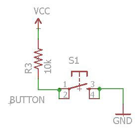
For this exercise, a 10 k pull-up resistor was selected.
- Connect digital output pin (labelled as LED below) to aquire current to LED (labelled as L1 LED below).
- Connect digital output pin as current sink or direct current flow.
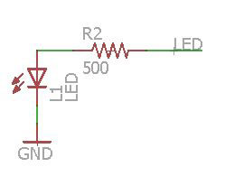
For this exercise, the digital output pin was configured to sink current from LED whenever it turns on.
Map of working process:
Download and install Eagle (if you haven't done so) > Download fab.lbr (Fab components library) from Fab Academy and insert in Eagle Directories > start Fab Academy tutorial.
Here are some of the critical steps and experiences. For details on various functions, refer to Sparkfun tutorial above:
a) Insert the fab.lbr into Eagle's component library by opening Eagle's Control Panel page and under Options, click Directories. In the Directories window, under Libraries, insert $EAGLEDIR\lbr;C:\EAGLE-7.5.0\lbr\fab. The first command ($EAGLEDIR\lbr) denotes the location of the default eagle library (seperated by a semicolon) and the latter indicates the Fab Library location. Once the fab library directory is loaded, it should be able to be accessed by clicking the "add" button.
b) Especially for beginners, the downsides of the schemetic design process in Eagle or any alternative softwares is the difficulty in identifying the appropriate components. To avoid the extra-mile, below is a list of required components and the title of each component in Eagle.
| Parts | Eagle Components Name |
|---|---|
| Button Switch | 6MM_SWITCH6MM_SWITCH |
| 500 ohm / 10k resistor | RES-US> RES-US1206 |
| ATMel ATTiny44 SOIC | ATTINY44> ATTINY44-SSU |
| ISP 2X3 Header | AVRISP> AVRISPSMD |
| 1uF Capacitor | CAP-US> CAP-US1206 |
| LED | LED> LED1206 | 20 Mhz Resonator | RESONATOR | 1x6 Header | FTDI-SMD-HEADER |
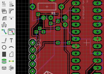
c) Once Schematic layout is done, the board layout should be displayed with components tucked to one side of the screen with thin yellow lines connecting each component. There will also be a bigger grey frame right next to the components. Follow the steps below to complete the board:
* Move every component into the big frame. The frame represents the dimensions of the board and can be adjusted by using the "move" function.
* Adjust and align each component in accordance to efficiency of spacing and routings should not cross one another unless they are meant to be connected. Use the "route" function for this section.
* Once routing is completed, double check on connectivity using the "DRC" function.
* Finally, create a frame around the board to isolate the entire board.
Test out different equivalent softwares
Software Downloads: Fritzing Upverter
Download generated Fritzing file (incomplete attempt): EchoHelloWorld.fzz
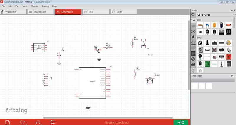
1) Fritzing
This is a user-friendly software and is capable of creating board designs in short period of time. The graphical representations of the components are excellent and ideal for identifying with the actual physical parts. The downsides of Fritzing is it's library. ATTiny44 cannot be found and the parts specified by Neil are missing as well. To complete the attempt to create an Echo Hello-world PCB board would require customization of parts. Attempt was aborted due to time constraints.
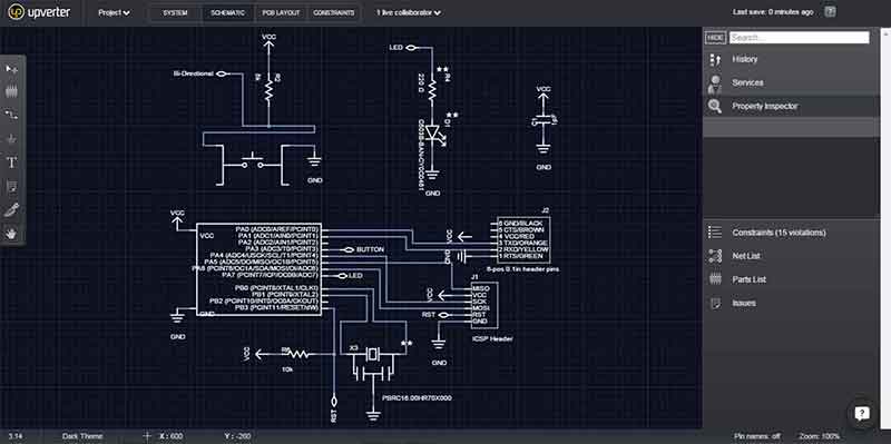
2) Upverter
This is an online program with user-friendly features as well. As compared to Eagle and Fritzing, Upverter perhaps strikes the middle ground between them in terms of features and library content. Following Natalia Papadopoulou's directions, ATTiny44 was found in the library and the schematic was almost completed until some errors were detected. Due to lack of knowledge on electronics, the attempt was aborted due to time contraints.
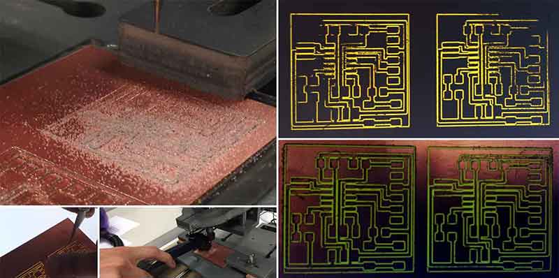
Milling
Miller model: PCB2020b
Download generated milling file: HelloTiny44_01.top.etch.nc (refer to top of page for eagle files)
Map of working process:
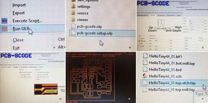
Export G-code from Eagle > Open up file in PCB-GCODE (miller software) to configure milling > Send file for milling > Platform calibrate miller > Mill!!
Here are the steps involved (shown in images below):
a) In Eagle, go to file and click "Run ULP"
b) Open the file "pcb-gcode-setup.ulp"
c) PCB-GCODE software opens up. Go to top menu and select "Machine". Ensure that the Unit (bottom left) is in millimeters (mm). All parameters set as default.
d) Next, go to "Operation Options" under menu and set the following parameters:
* Top side: Check "Generate top outlines" and uncheck the rest.
* Bottom Side: Uncheck all.
* Board: Check "Show Preview", "Generate milling, Prefer climb and Single pass. Uncheck the rest.
Key in the following:
* Width 800 * Depth -0.18 * Depth -0.127 * Depth -0.2794 * Minimum 0.12 * not used 0.508 * not used 0.127
e) Software will generate a preview. Observe the indication of passes on the extreme right of the screen. It should indicate as 1 passes. Go back to step 4 again to if it is more tha 1 passes. This will ensure that miller will only run 1 layer of cutting.
f) Once settings are confirmed, save file and run it in miller operation software.
g) Platform Calibrate Miller
Here are the steps involved (shown in images below):
1) Setup printer shown
2) Move cutting tip to the bottom most corner using the printer software
3) Visually gauge the tip's position. Position it so that it doesn't hit the mounting clamps
4) Place a piece of paper between the tip and the PCD board. Move the tip (z axis) until the paper can't be moved. This would be the zero or the point where the miller starts cutting.
5) Check the circle at the left of x,y and z-axis to confirm zeroing. Try other parts of the PCB board to see if there's any other points that has a zero lower than this one. Choose the one that has the lowest settings.
6) Select "play" to begin milling. One good way to check whether if the miller has cut deep enough is to witness the amount of copper dust landed on the surface during milling.
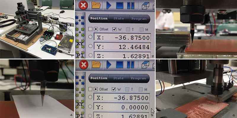
7) The milling took a few rounds to achieve a reasonable standard to proceed with stuffing components.
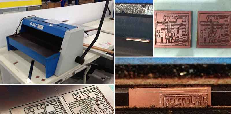
8) Final touch-up using a GMC cutter to trim up the boards. Scorelines were done using either a pen knife or a steel ruler. Next, align the scorelines with the cutter edge. This has to be done by viewing from the top of the machine where the gap is located. Finally, lower the lever to cut the boards.
Stuffing
Stuffing is perhaps the easiest to document but the hardest to practice. Here are some of the difficulties faced during the process:
* ATTiny44 has many connecting points and they are very close to one another. Soldering needs a lot of care to avoid short circuiting. ATTiny44 is polarity specific. Make sure the dotted end is facing the right direction.
* Button switch will not fit the board if the legs weren't bended.
* 1x6 Header needs to be fully rested on the board. This has to be done by making sure that the black plastic component is placed flat on the board.
* LED breaks easily. Ensure that they are fully checked for operation before attempting to solder. To check, simply use multimeter to touch both ends and see whether if it lights up. LEDs are polarity specific as well. Make sure the green strips end is facing the track connected to the resistor.
Reflections
This week has proven to be a little more challenging than what was expected. Quite a fair bit of time was spend on experimenting different softwares which ended up documented as abortive exercises. Also, the milling took longer than expected due to several adjustments during the process to attain good milling standards. Finally, during stuffing of components, some LEDs were damaged and had to be re-soldered.
All in all, the week has been challenging but exciting to see another PCB board produced. This time it came with a button and an LED light. Cool!

Related Projects