week 03 | 2016/02/17 - 2016/02/24 | electronics production
17
Stage 3: Soldering, initial startup
18
Welcome to the third and last stage! Heat up your soldering iron and grab fine solder!
19
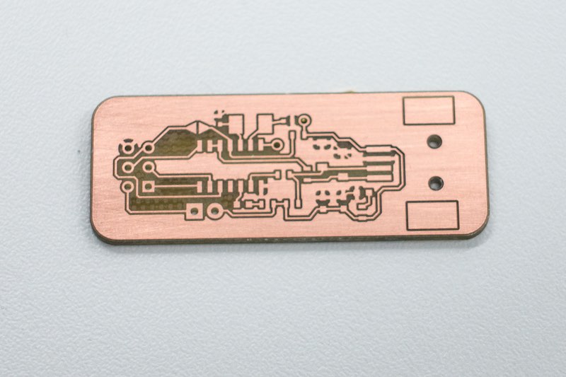
After cleaning the PCB, I coated my PCB with solderable PCB varnish to protect it from oxidation.
20
Top layer coated
21
22
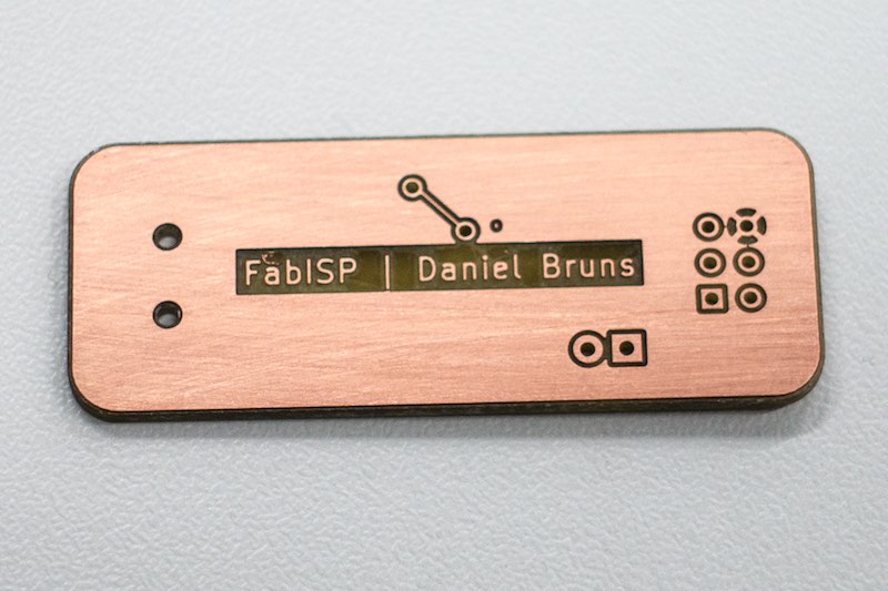
Bottom layer coated
23
24
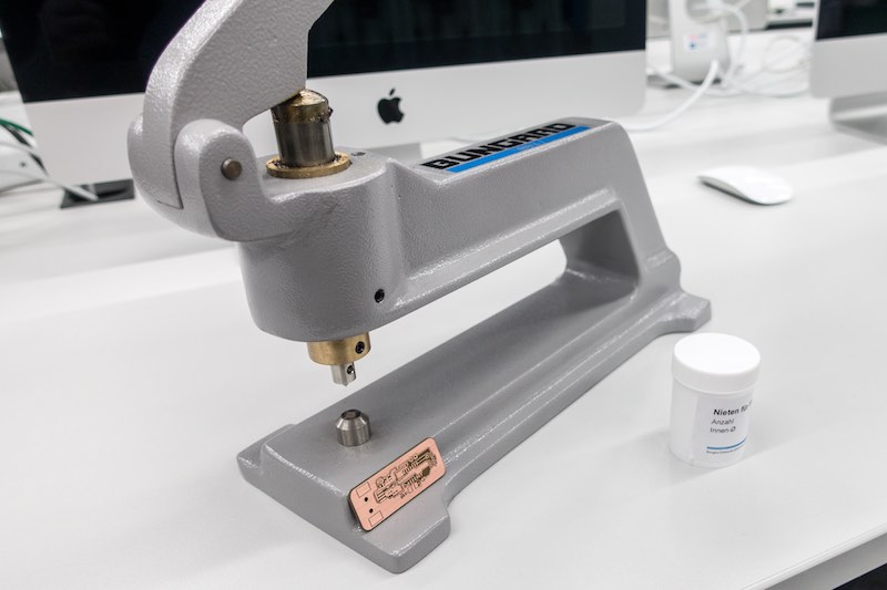
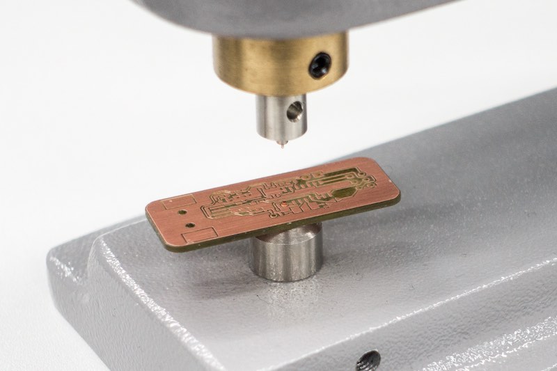
To connect the top with the bottom layer circuit paths, I had to use 0.6mm rivets with our toggle lever press.
25
26
Just insert the rivets into the hole, align the pcb on the punch and press with reasonable pressure. To secure and protect the connection, I soldered the rivets additional to my PCB.
27
28
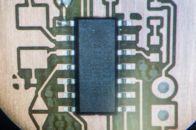
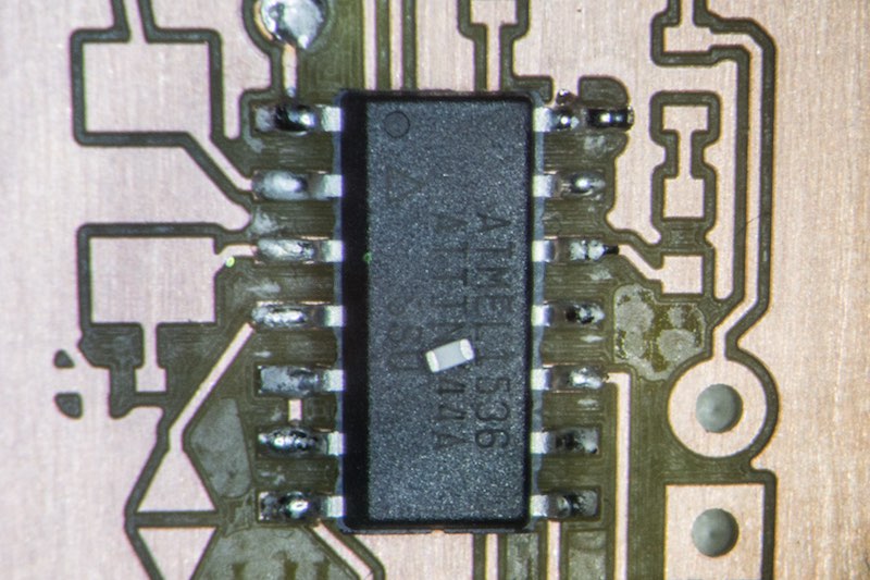
Due to the fact that I used a lot of small 0603 and some 0402 parts, I had to follow a wise sequence of soldering to not block following parts. I started with the ATTiny. First, I soldered one pin in one edge to fix and align the ATTiny, then I soldered the remaining pins. To solder the first pin, add some solder to your pad on the PCB, press and fix the ATTiny down and align it with tweezers - then heat up the pin and pad. Not that complicate :)
29
30
Just for fun - a comparison between the ATTiny and my 0402 18pF capacitors for the crystal.
31
32
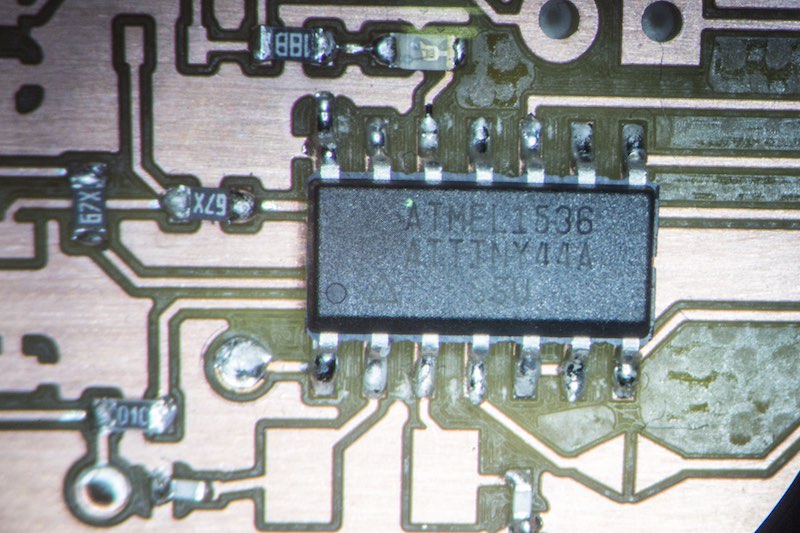
Solder from the middle to the outside, from low to high parts. Use the tweezer method for fixing the parts...
33
34
This is my programming soldering jumper in closed position :)
35
36
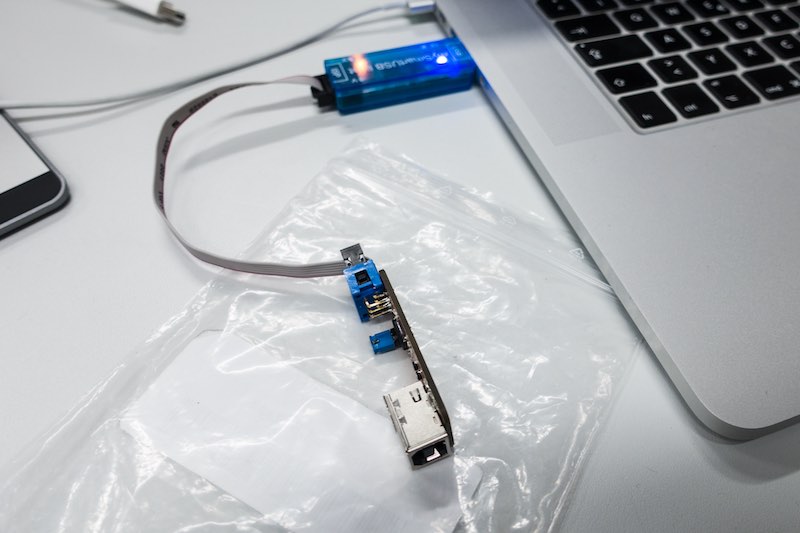
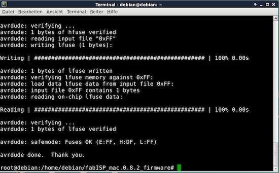
Befor using my FabISP I had program it with another ISP. For this step, I followed Anna's tutorial, compiled the firmware with some additions and flashed my FabISP.
37
38
Instead of using the normal given firmware, I added some features. I changed the device name to HRW FabISP and added the code to use the second LED, which flashed until the USB connection is enumerated, then turns off. When the ISP is preparing SPI commands and while flashing other hardware, the LED is even on.
39
40
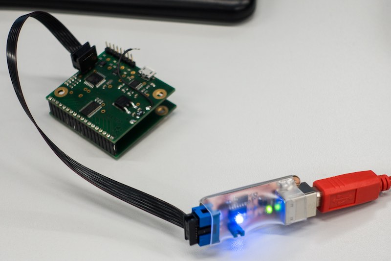
Finished :)
41

This work by Daniel Bruns is licensed under a Creative Commons Attribution-NonCommercial-ShareAlike 4.0 International License.