week 03 | 2016/02/17 - 2016/02/24 | electronics production
15
Stage 1: Schematic, create parts/footprints, routing
16
Welcome to the first stage!
17
After installing KiCad I opened the documentation which is very helpful for a absolutely noob in PCB design. The first step is creating a project - I created my project folder directly into the FabAcademy GIT.
18
The next step is creating the schematic. Now it's the time to add all needed parts like microcontroller, resistors e.g. to the schematic and seperate them in reasonable groups.
19
20
While editing, you have to assign the right footprints to your parts. Just make a right-click on a part, choose properties and search the proper footprint in the library.
21
22
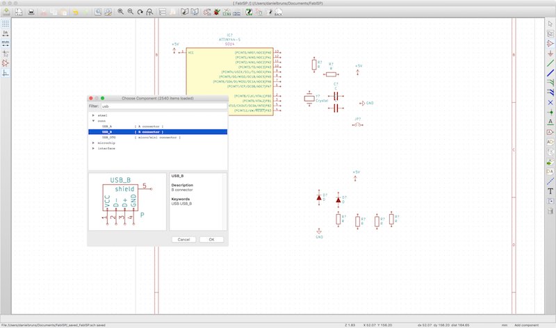
Some parts later, you'll get the first problem automatically - you want to use a part, which is not included in the general KiCad library. So it is your turn to generate a library (a seperate for your project or your own general additions). The first part which was not included was the USB-B connector I wanted to use. - I thought this was the right way to use KiCad, but it wasn't. KiCad seperates schematic symbols from footprints. In my case I only had to generate a new footprint, because the pins were the same. Don't think about it - it was my first time... But as conclusion: generating new parts is easy. :) Just click on the library editor and add a new part, then add or change the values.
23
24
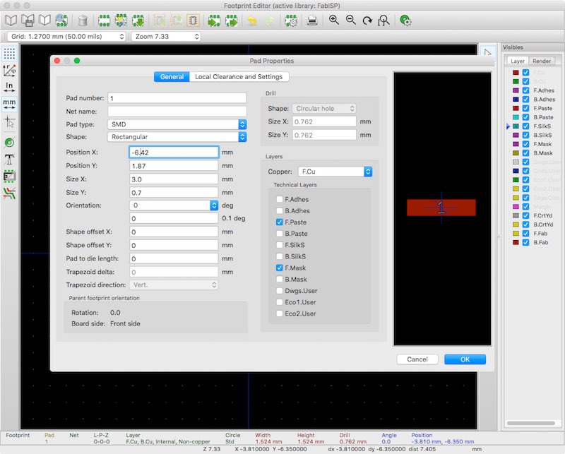
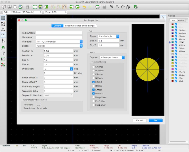
The right way in this case, is just generating a new footprint in the footprint editor. Before using the footprint editor, you have to generate a new footprint library and add the new library in the footprint library manager in the properties of the footprint editor. The KiCad tutorial helped me a lot at this point. After generating the new library, create a new footprint, then click on add pads. The new window which appears shows the pad properties, where you're able to change all the needed settings like pad number, which must be identical to the drawing in the corresponding datasheet, pad type, which defines the type of the pad, like SMD, through-hole, non-plated through-hole mechanical etc. . After setting the number and type, the dimensions and positions must be set. You have to do this in a simple cartesian coordinate system for every pad you need. The last thing for the pads is to assign them to the right layer. I'll show you two diffent pads I created for my USB-B connector. The first one is a normal rectangular SMD pad.
25
26
The second pad for my USB-B connector I would like to show, is one of the mounting holes. This one is a mechanical hole which must be drilled. As you can see, it occupies the bottom layer as well as the top layer.
27
28
Now it is time to add a footprint contour for the silkscreen. Click on the line or circle button and align them correctly in the already used cartesian coordinate system.
29
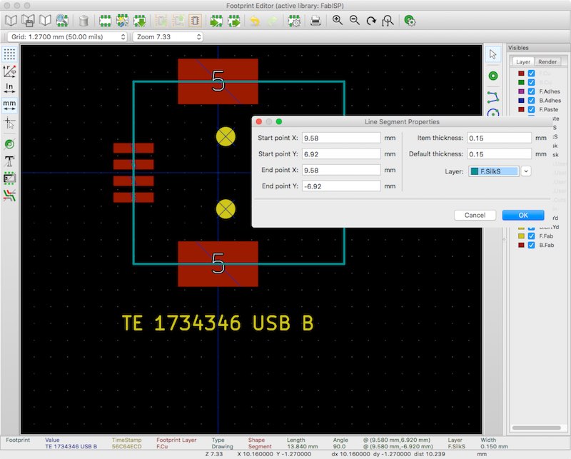
30
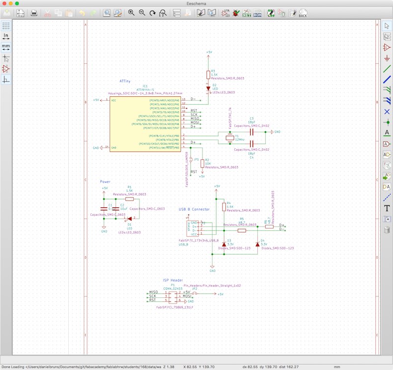
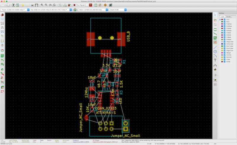
After adding all needed parts, footprints and connecting them to reasonable circuits, the schematic will look like this:
31
32
The next step is to align the parts wise, for example to reduce the length of data circuits, avoid crossings and bring the PCB into the shape you need or want. After exporting the Netlist from your schematic into the PCBnew part of KiCad, you'll get a bunch of parts in the middle of your screen.
33
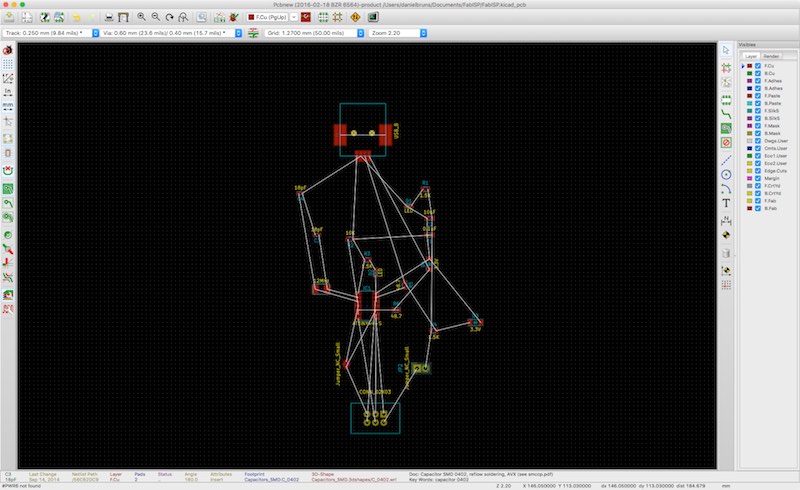
34
All the white lines you see, are points you must connect and route the circuit paths between. These white lines only show the next possible connection. Don't be shy to push them around, the white lines will always show the nearest possible connection. After unraveling the parts and paths, my PCB looked like this:
35
36
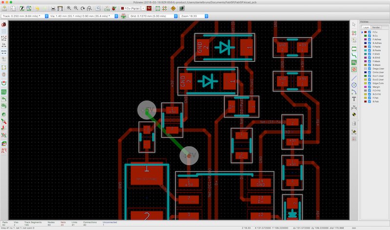
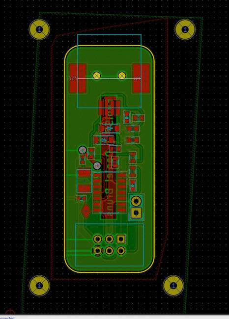
With the routing tool, I started routing the paths. This step took me a long while the first time. I had to realign my parts several times to avoid unwanted crossings or shapes. After routing all paths, there was only one path which ruffled up a bit. I solved this problem by adding two vias. This step gave me the chance to route this path on the bottom layer. Actually my plan was to use only one side but this path had to cross too much other paths. I had the choice to add some 0 Ohm resistors as bridge or apply a via or through-hole connection. As through-hole connections are possible to made with every drill and a cable, I chose this option to save some space. The red lines show paths on the top layer and the green lines show the path on the bottom layer. The grey circles show the vias.
37
38
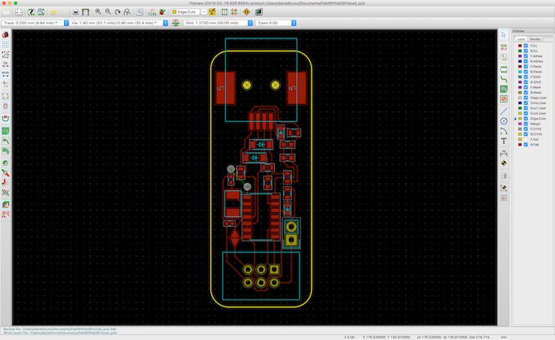
This is my final PCB design. As you can see, the yellow line is the shape of my PCB.
39
40
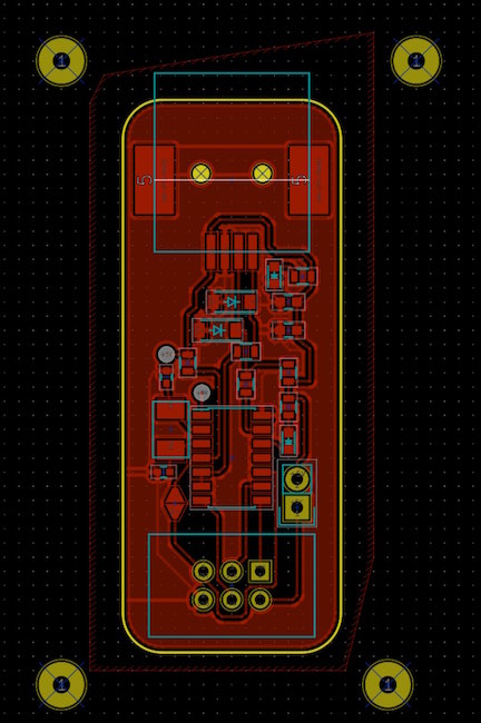
Now we have to add a ground plane to both sides and insert some fiducial marks which the PCB mill needs to orientate itself after turning the PCB while milling. KiCad offer a simple tool to add a ground plane, just make a right-click and use the fill/refill all zones tool. This tool uses the inserted or given values for path or track width, via diameter, part dimensions etc. and their clearance to calculate the shape of the ground plane. This is my PCB after adding the ground plane (red= top layer, green= bottom layer):
41
42
43
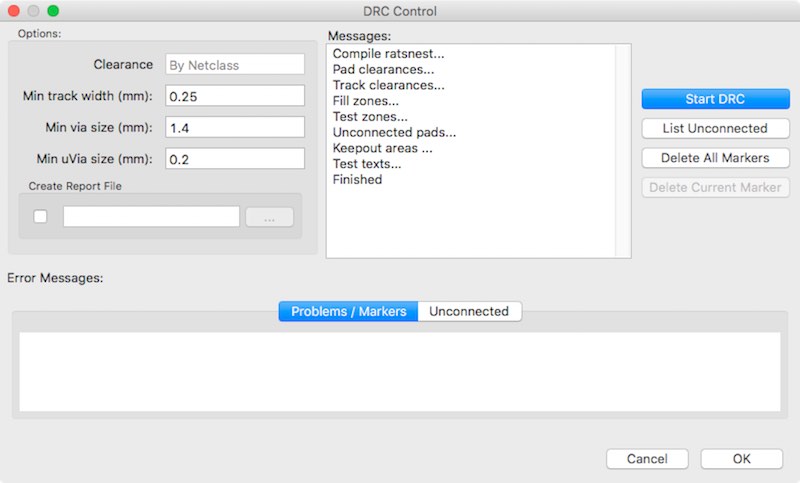
The next to last step before exporting the files into Gerber, is to do a design rule check. This tool checks if your PCB is in the given range of values for example of pad clearance or if there are unconnected pads. I had no error messages, so I was able to export my files into Gerber to mill my PCB.
44
Oh, it's a long way up - take this shortcut to stage 2!

This work by Daniel Bruns is licensed under a Creative Commons Attribution-NonCommercial-ShareAlike 4.0 International License.