Assignment:
A_Redraw the echo hello-world board + Add (at least) a button and LED (with current-limiting resistor.
B_ Check the design rules, and make it.
Redraw the echo hello-world board.
I did this exercise last year but I will repeat it from scratch to get more comfortable with datasheets and components.
A_Redraw the echo hello-world board + Add (at least) a button and LED (with current-limiting resistor.
Geting ready.
I have watched quite a few tutorials from Sparkfun and Jeremy Blum to get more familiar with the workflow as well as to better assimilate basic electricity and electronics concepts. I am still very green and still cannot imagine how I could design a board from scratch. I am not prentending to be creative in any ways with this exercise but acquiere technical skills.
I use this tutorial to refresh my memory since that is the board I had done last year.
This time I am going to make a Attiny44 that uses the copper layer as ground (GND) using this documentation. This document explores different options of applications such as Kikad and Kokopelly but after reading about them I decided to stick with Eagle and move on to make the board.
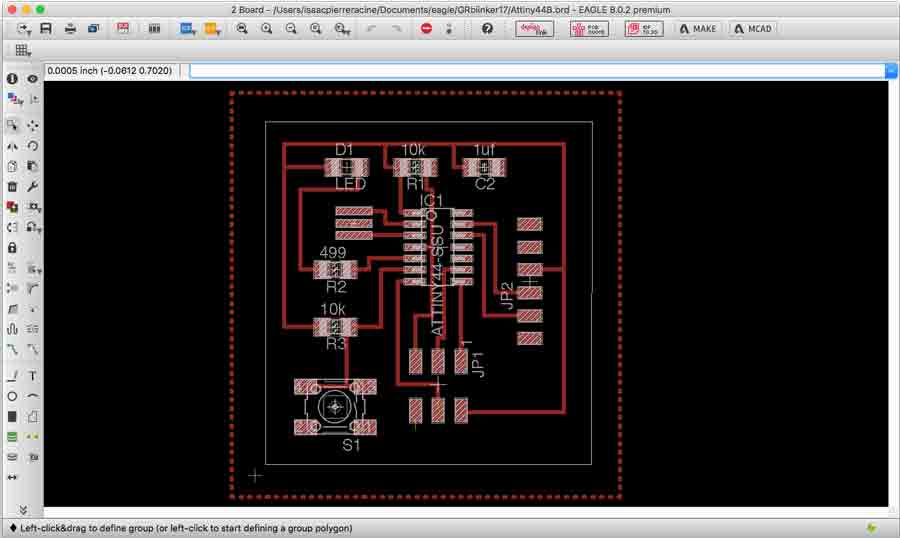
1_Drawing the board + Add (at least) a button and LED (with current-limiting resistor..
I followed the instructions on the tutorial to make the schematic but once completed the board did not connect properly. I struggled a while until I realized that I had labeled the components using the text command instead of the label/name. Once I labeled and named them properly the ground connections still did not connect right so I went back to the libraries and changed the ground symbol I had used to another one. That made it work.
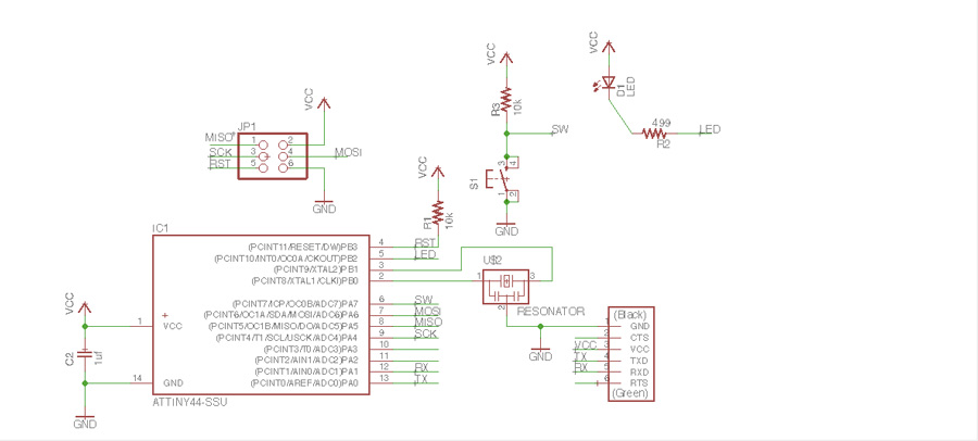
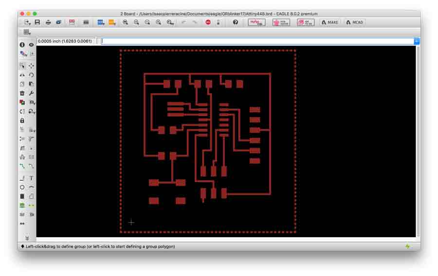
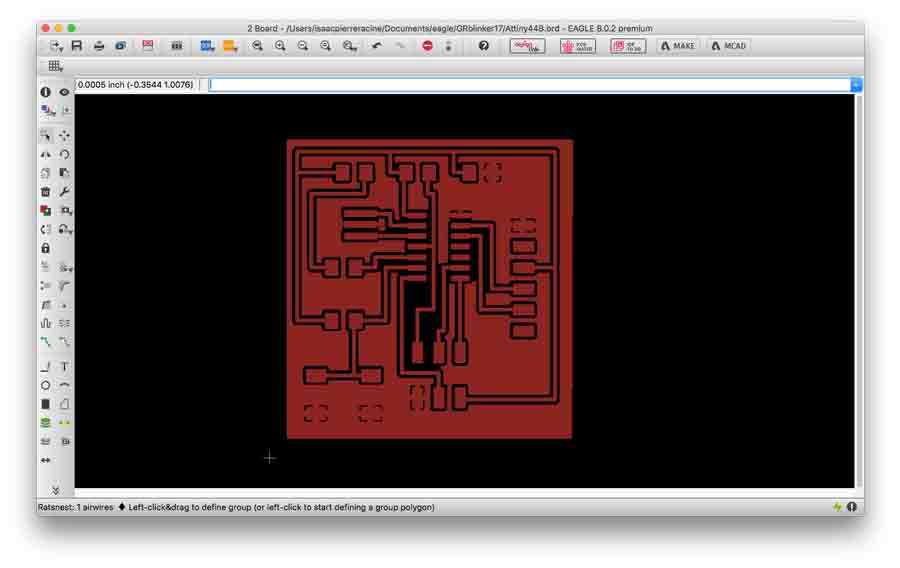
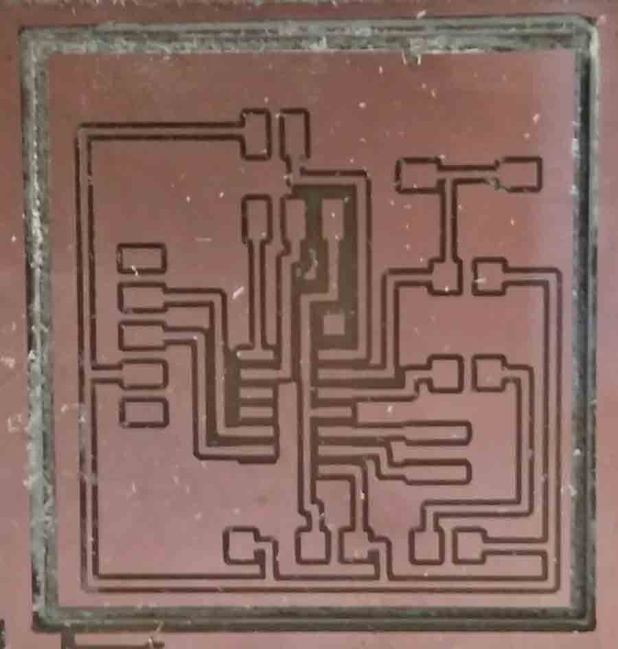
I did all the tracing of the connections and connected the ground to the copper layer of the board creating a rectangle outside the white limit frame using the polygone command, naming the rectangle as ground (GND) - this converts the rectangle lines in dots - and than using the "rastnest" to make the base layer as GND. This operation makes the base of the board go red.
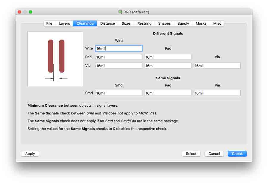
B_Check the design rules, and make it.
The tutorials recommended to set clearance at 12mm in the design rules but I decided to set them at 16mm. to be safer. The DCR (design rules) check was succesfull as it detected no errors.
Exporting the file from Eagle to PNG (file menu/export/image) went pretty fast at first but got complicated as I was told the new version of Eagle (8.0.2) has a bug and do not respect the original size of the board. I first exported a version to PNG (making shure the monochrome option is clicked on so the image is converted to black and white). Than I opened it in Photoshop. The PNG opened as an index file so it needs to be convert into a grey scale image so it can be editied. The editing of the image consists in creating 2 separete files: one for the trace and another one for the outline.
The is done by cropping the image leaving a small frame around the limits of the boards (the frame should be at least as wide as the vias of the board), and add a white background layer the same size of that frame. Each layer has to be exported as individual PNG files.
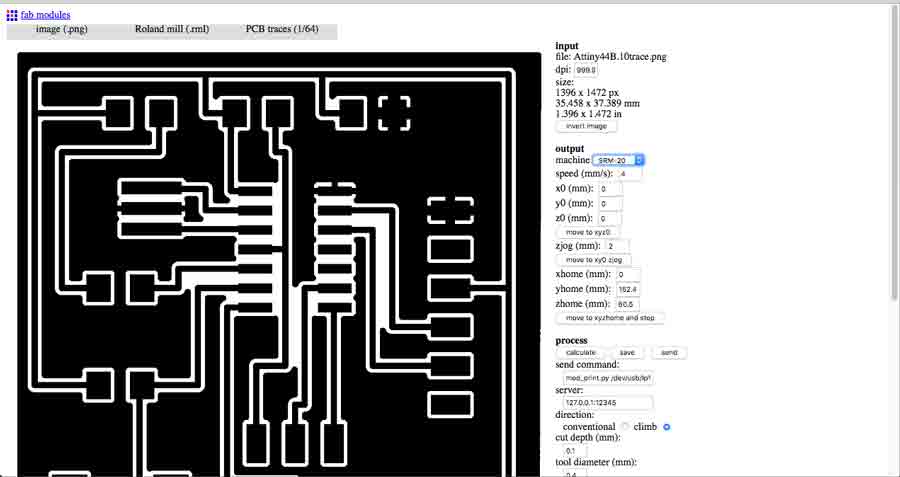
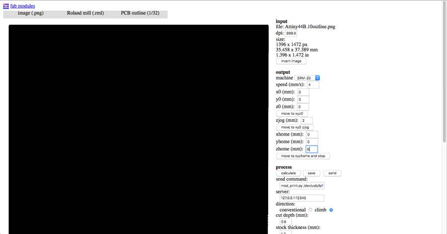
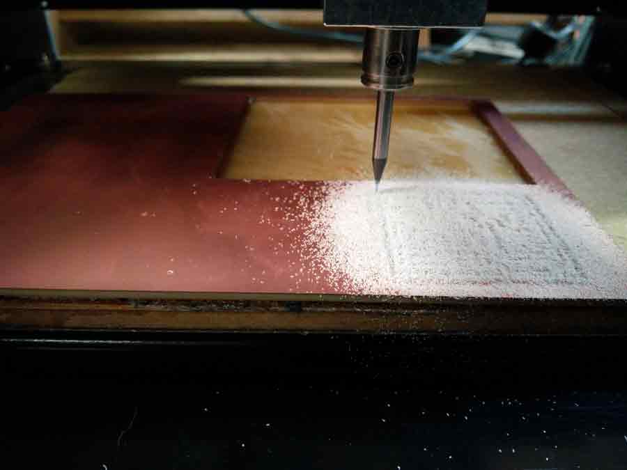
Milling the board is usual business: open the file in the fab module, set the parameters on the module, prepare the copper board on the Modela bed and set the axes (X/Y and Z). The firt intent did not come out well as I did not realized I had to invert the image when milling a board designed with the copper layer as GND. I repeated a 2nd time but it neither came out well because the board was too small and part of the milling area was out of the board. I repeated it and again it failed. For some reason (could not find a logical reason except that I must have made a mistake and choose the wrong file when loading it to the fabmodule) so the outline file did not lined up properly with the trace file therefore cutting the traces on one side of the board.
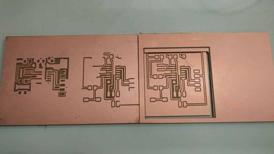
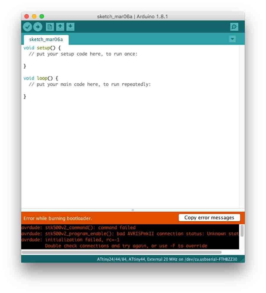
Before going on milling another board I wanted to hack my failed board using cable to bridge the traces that had not been milled. I spend a lot of time working on soldering the components and bridging the VCC vias but I could not make it to work. I liked the idea to make a board that was everything but orthodox so I persevered in trying. I got a green light from the programmer but when I configure Arduino to program the board it gave me failure message. I identified some short-circuits and tried to resoldered but it became really messy so I surrendered and decided to mill a new one.
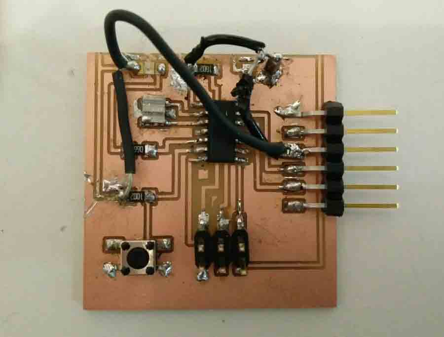
At last I managed to mill the board and it came out much better. I did the milling at Green Fablab and there were no double-face tape so I had to invent a way to hold the board to the machine bed. While doing the tracing it moved a little bit but did not make any dammage.
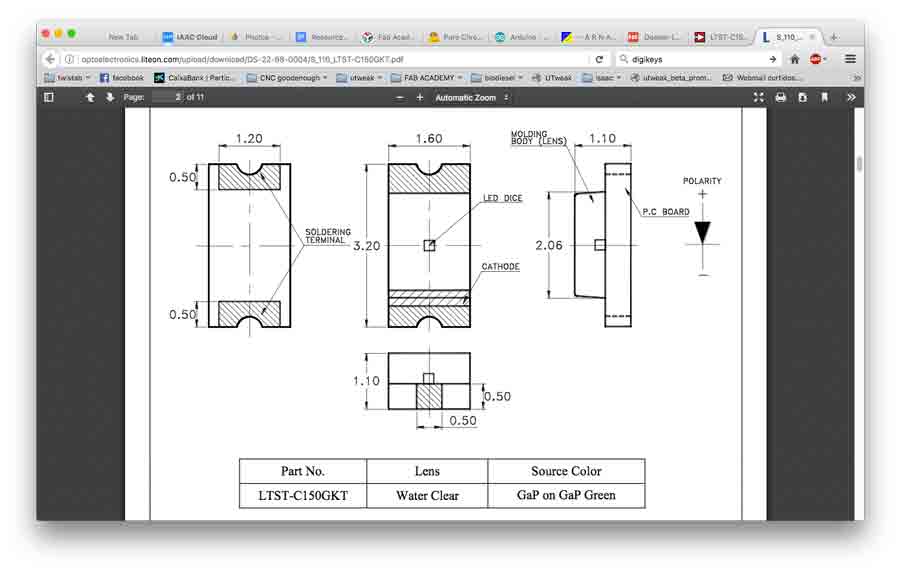
When It came down to soldering I had doubt about in which direction to soldier the LED so I went to the datasheet and comfirmed it: there is a a tiny green stripe on the cathode (-) that has to be connected to GND and anode to VCC.
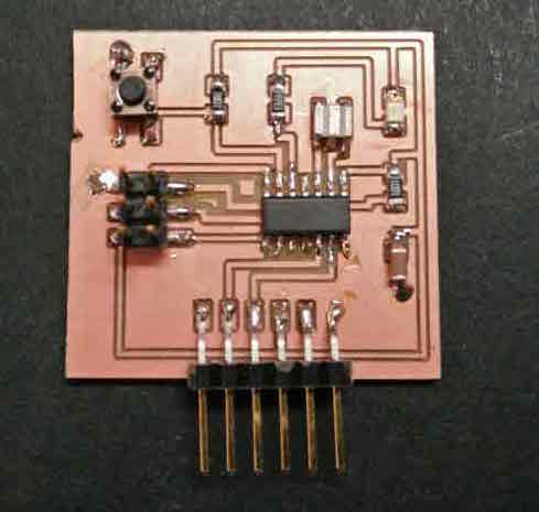
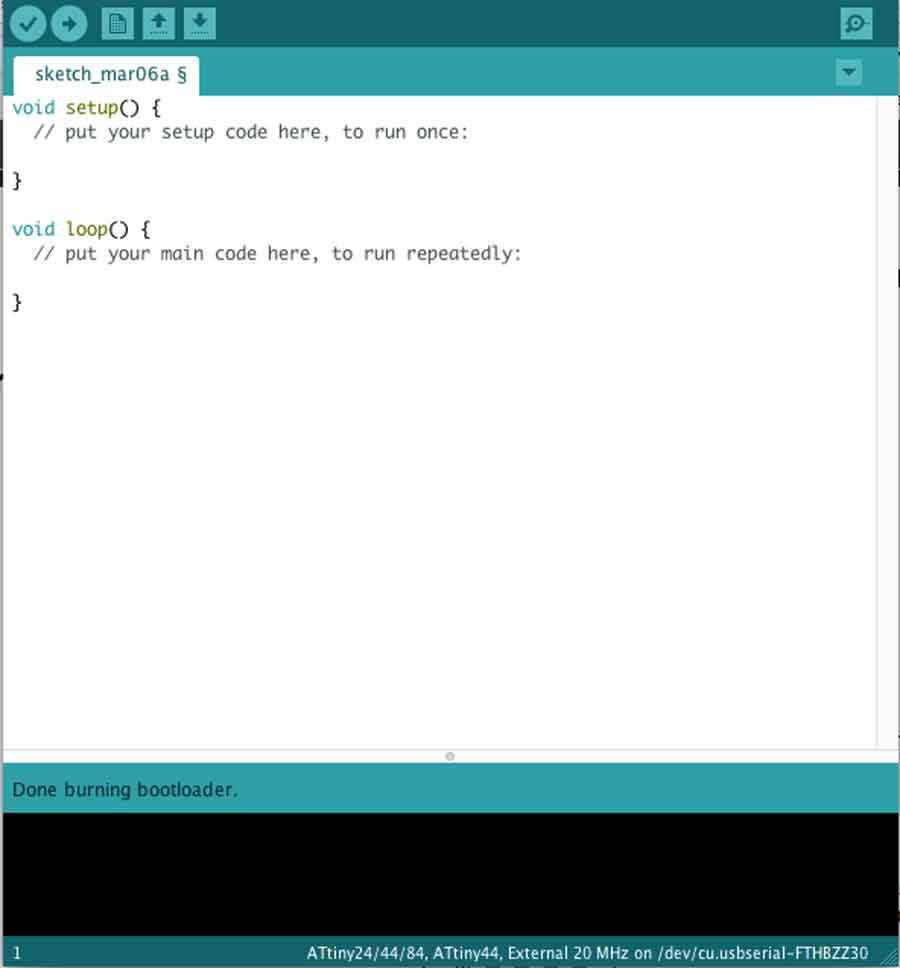
I tested the board and got a green light from the programmer. Then I connected it to my FabIsp and did the check up using Arduino and got a succesful result.
The board is tested and ready to be programmed for the next electronic assignment. This week helped me get more familiar and comfortable with the electronic design workflow (schematic and board), the components, milling and soldering. I feel very satisfied with the experience.