PCB Milling
This week our task is to create a Printed Circuit Board, solder all the components and burn the code into it. The designs and code have already been provided to us. The main intension is to develop our soldering and debugging skills.
Printed Circuit Board (PCB) is a mechanical assembly consisting of layers of fiberglass sheet laminated with etched copper patterns. A PCB, holds an electronic circuit together. The completed PCB with components attached is a printed circuit board assembly, or PCBA. PCBs can be single sided (one copper layer), double sided (two copper layers) or multi-layer (outer and inner layers). A multilayer PCB may have as many as 10 stacked PCBs. For this task we are using a single sided copper claded sheet during milling our PCB.
There are many different ways for creating a PCB, such as etching, direct plating, copper removal or milling, etc. We are using a Roland Modela MDX-20 for the creation of PCB via milling process. This method is not the industrial process of creating PCBs but is suited just for prototyping.
A small intro to In-System Programming (ISP) also called In-Circuit Serial Programming (ICSP), since we will be building a ISP for this weeks assignment. ISP is the ability of some programmable logic devices, microcontrollers, and other embedded devices to be programmed while installed in a complete system, rather than requiring the chip to be programmed prior to installing it into the system. It eliminates the physical removal of chips from the system. This will save time, and money, both during development in the lab, and when updating the software or parameters in the field.
Designing the PCB
The designs and code for creating the ISP have already been provided. Some ISPs that are provided were created by Brian, Zaerc, Ali, Valentin, Andy, David; of which I decided to replicate the ISP done by Brain.
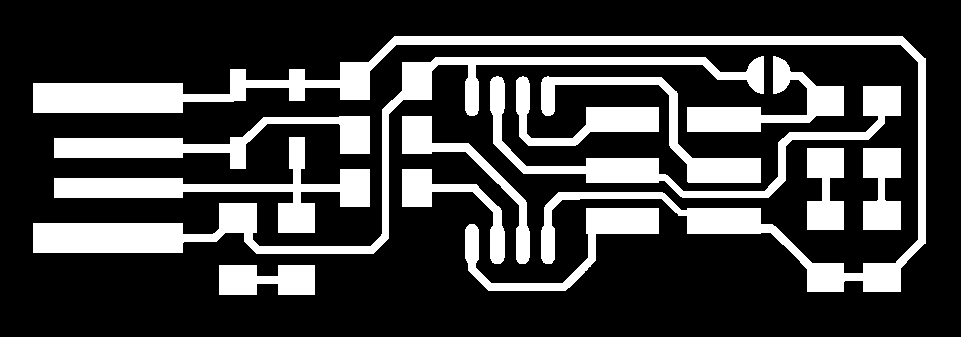
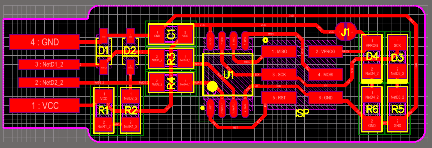
The schematic and the traces for Brian's design of in-circuit programmer.

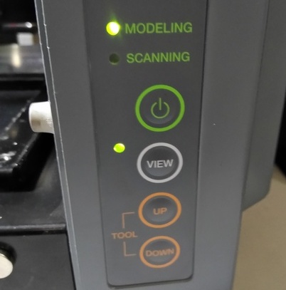
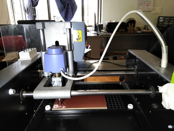
Description of Roland Modela MDX-20
The machine is a table top PCB milling device. It creates the PCB design by milling away all areas what are not needed for creating the circuit trace. From the trace image, the white areas are retained the black areas are milled away. It has a base plate which can be removed easily by removing the screws. The base plate is metal and moves in y-axis. The head of the machine moves in x-axis and the section that holds the drilling bit, called the end-effector moves in z-axis. Following pictures are of the machine, its control panel and milling head.


Setting and Cutting
We use the Fab Modules to convert the design files to tool vector path. We already used this software last week. Make sure you select the machine and load the design file. Select the milling trace bit size, we use the 1/64 th inch (0.4 mm) size bit for milling traces and 1/32 th inch (0.8 mm) size for milling the board. Make path creates the vector tool path. I set everything to defaults.
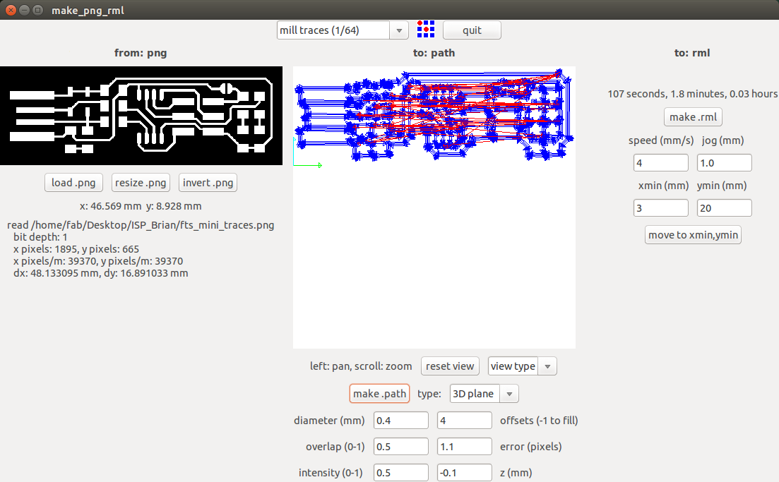

Offset is the number of times the machine mills a path and remove those areas that are not needed for creating the trace.
Overlap is the percent of area you want the machine to overlap previously milled area on its next milling line.
Intensity is the depth by which the end-effector drills down, it is set to 0.1 mm.
The drill bit has a joging distance of 1mm or a step
To remove the base plate, click View on the control panel and remove the screws on the plate. The image below shows the base plate that is removed with a sacrificial layer placed on it.
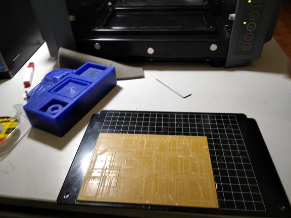
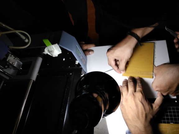
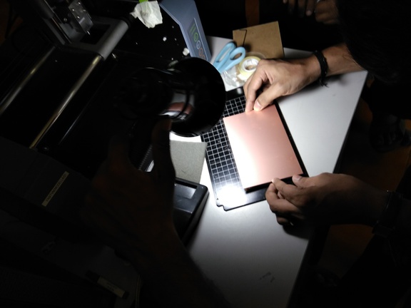
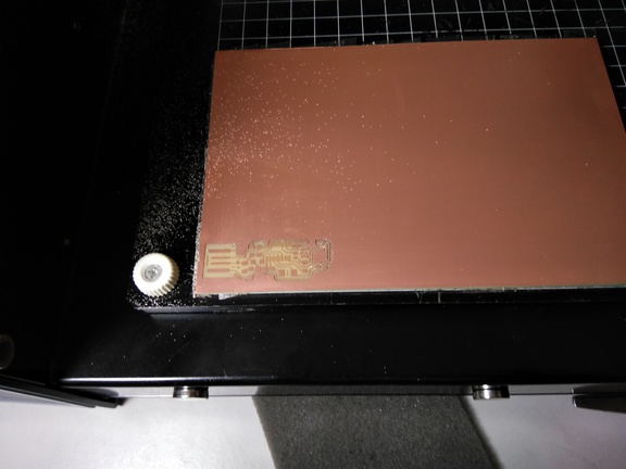
We need to make sure our copper cladded sheet does not move around when the milling is underway. So we stick double sided tape on the bottom and stick the sheet on the sacrificial layer. Make sure there are no flexes and the sheet lies flat on the base plate.

After these steps, place back the base plate on to the machine and tighten the screws.
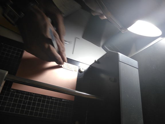
The next step is to set the origin for the head to start the milling process. Make sure the drill bit is placed deep into the head unit, so that only a small part comes down. This step is to make sure we do not accidently brake the bit. Then move the head to an origin by using the Fab Modules move xmin, ymin, by trial and error, you can a set the origin point. Once that is set, use the allan key to loosen the bit and make sure, it just touches the copper claded sheet. Then tighten it up. We have origin set.


Click make .rml to send the vector path to the machine and it opens another window showing the progress of the task. There is abort button on the UI, in case there is some sort of emergency such as broken drill bit.
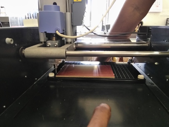
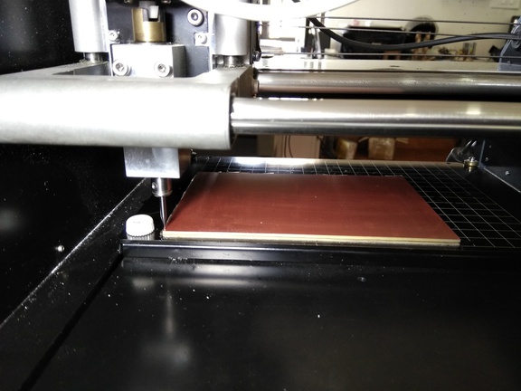
Pics when milling is underway


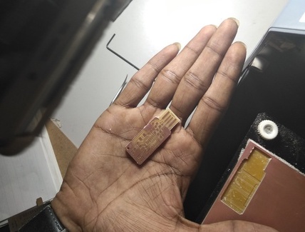
With the same origin set again, use the Fab Modules and change the settings of the drill bit to 1/32 th inch for cutting the PCB. And the load the cutting trace to it. Repeat the same process mentioned above to cut out the PCB.


Assembling the PCB
I used the PCB design file, that was provided to identify all the components and solder them to the PCB in their rightful locations.
The following parts are needed to build Brian's version of the ISP programmer, fabTinyISP.

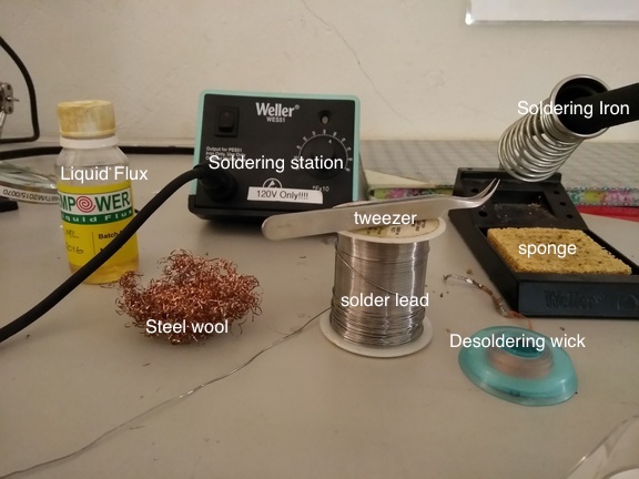
Rest of the process is simple, solder all the components accordingly. Our instructor gave us a useful tip to solder. Heat the copper pad, and apply lead and then place the legs of our components and resolder it. I found this tip to be extremly helpful. I was able to solder the components without any trouble. Its important to keep the air filter running during soldering process. You do not want to breath in the toxic fumes. Use tweezers to hold the SMD components during soldering, neither do you want to loose these small stuffs nor do you want to burn your fingers.

Hero shot of my PCBA fabTinyISP

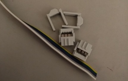
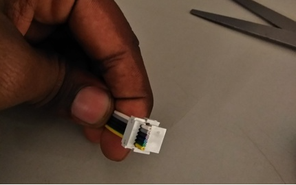
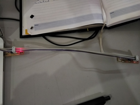
My IDC ISP cable.

Debugging
Once soldering is completed, make sure all the components are soldered properly. And short the jumper. Use the multimeter to test the connectivity of the components. I did not have any loss of connectivity to my components, when I tested using the multimeter, so I plugged the device to the USB port of my computer. Since Brian's design included an Red LED, that reconfirmed that power comes into my circuit when it lights up.
Programming fabTinyISP
Brian's documentation clearly states what the process we have to carry out in detail. I connected another ISP that works, to my PCBA using the IDC ISP cable and connected the working ISP to my mac machine. If all the connections are good, then both the devices will light up.
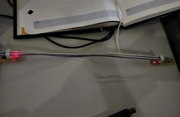
Also make sure the Pin 1 of one ISP connects to the same of the other, else it might not light up. The following is a picture showing when Pin1 on ISP is not connected to Pin 1 of PCBA
I downloaded CrossPack and firmware source code into my mac. And updated Makefile
PROGRAMMER ?= usbtiny in the firmware source code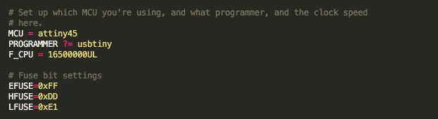
I then went to the directory of the firmware source code and ran
make. But it errored.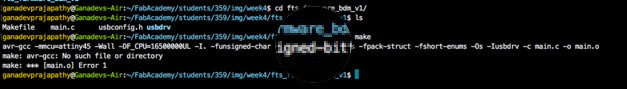
I later figured out, even though I installed CrossPack, the terminal was not reflecting the change.
So I reopened the terminal and then it worked. It created .hex file.
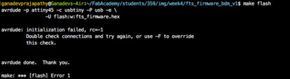
I then ran
make flash. This will erase the target chip, and program its flash memory with the contents of the .hex file you built before. I should see several progress bars while avrdude erases, programs, and verifies the chip. But I was encountering another error.
I ran again.
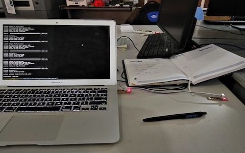
I found out the ISPs were not getting detected. There was some loose connection with the ISP and my USB. I opened the console.log in mac to find out if the ISPs were being shown. The following screenshots show when the ISP gets connected.

I was finally able to flash it and ran
make fuses. This errored due to connection getting disturbed, which we detected earlier.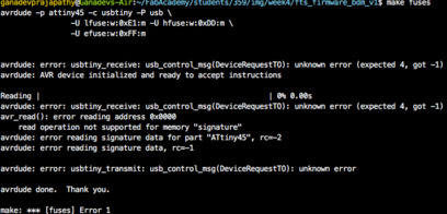
Ran
make fuses again. This will set up all of the fuses except the one that disables the reset pin.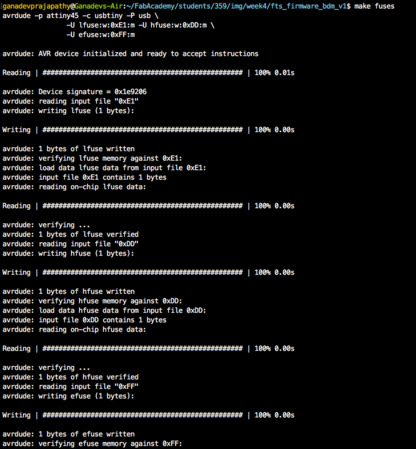
Ran
make rstdisbl. This does the same thing as the make fuses command, but this time it's going to include that reset disable bit as well.
I was able to use my ISP to program another ISP of a collegue here at FabLab. I was able to see GREEN LED light up when my ISP was burning code into the other PCBA. But sadly, I did not take a snap of the event.