This week our assignment was to design and build a wired &/or wireless network connecting at least two processors
Embedded communication is the process of sending information between two MCUs or from one circuit to other. For a communication to happen there needs to be a transmitter and a receiver. Communication may be in one direction or in both directions, there are different classifications according to this, but the basic classification is Synchronous and Asynchronous communication.
Synchronous: means sender and receiver use the same clock signal. Asynchronous: means sender provides a synchronization signal to the receiver before starting the transfer of each message.
A communication protocol is a system of rules that allow two or more entities of the communications system to transmit information via any kind of variation of a physical quantity. Communications protocols cover authentication, error detection and correction, and signaling. They can also describe the syntax, semantics, and synchronization of analog and digital communications. Communications protocols are implemented in hardware and software. There are thousands of communications protocols that are used everywhere in analog and digital communications.
Communications devices have to agree on many physical aspects of the data to be exchanged before successful transmission can take place. Rules defining transmissions are called protocols. There are two main categories in this.
1.Inter System Protocol
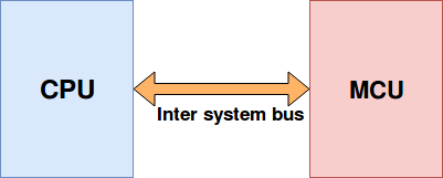
This is used to communicate between two different devices like a communication between a computer and microcontroller. It uses a dedicated bus to communication.
Different Inter system protocol:
2.Intra System Protocol
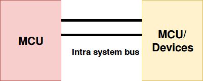
This is used to communicate between two devices within the circuit. The circuit complexity, power consumption will be less in this.
Different Intra system protocol:
This is some basic information about embedded communication, which I got while researching online.
This week was a really tough week, I was completely clueless after watching Neil's lecture. I did not have a clear Idea of what I wanted to do this week, hence I first started reading about the various communication protocols and methods. Even after three days of solid reading I got nowhere. I understood only parts of each protocol, but the problem is that I don't know how to implement it.
Most of the time I was running around the lab like a headless chicken. It would take me days to properly understand the protocols to implement them correctly. Hence finally I decided to look at some Arduino tutorials for communication and came across I2C. Some of my friends were also doing it, so if something goes wrong, they might be able to help me.
My original plan was to implement the touch sensor I made in inputs week and then light an LED of a board when I press the touch pad. But through the course of the week I was not able to do that. This week was entirely spend on troubleshooting.

I2C is a serial protocol for two-wire interface to connect low-speed devices like microcontrollers, EEPROMs, A/D and D/A converters, I/O interfaces and other similar peripherals in embedded systems. The bus has one clock and one data line.
The easy implementations comes with the fact that only two wires are required for communication between up to almost 128 devices Each device has a preset ID or a unique device address so the master can choose with which devices will be communicating.
The two wires are called Serial Clock (or SCL) and Serial Data (or SDA). The SCL line is the clock signal which synchronize the data transfer between the devices on the I2C bus and it’s generated by the master device. The other line is the SDA line which carries the data.
I decided to make a slave board similar to the example given by Neil. I would then talk to it using the satsha kit I made in Inputs week.
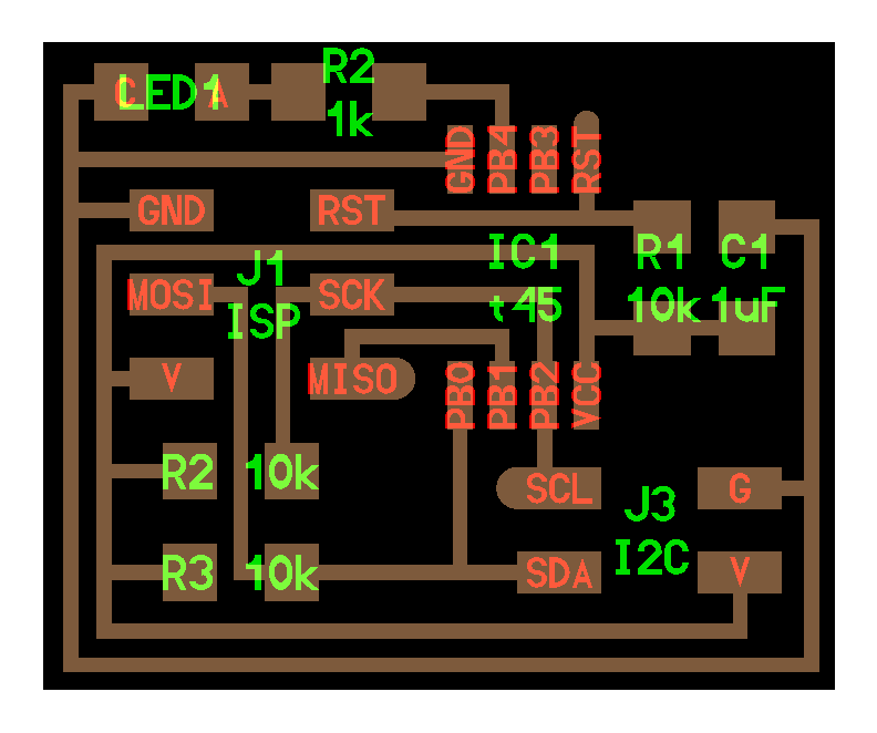
This is Neil's Node board, here the SCL and SDA line have a pullup resistor so that the line will always be high.
I started designing the board in EAGLE. I used Neils board as a reference and make the drew the schematic for the node.

Once the schematic is done, I switched to the board view and arranged the components of the board and started routing them. After some time I finished routing the board. This was a tiny board and routing was simple compared to the other boards I have done before.

I exported the file from EAGLE as a png.

This is the final board I designed, I added an extra LED to an unused pin PB3.

This is th cut line for the board.
This time I wanted to try something different. I'm going to mill the board in Shopbot. The reason I wanted to do this is because I was curious how it would turn out and I wanted to learn how to do that in case of an emergency. We had broken 5 1/64" bits for Modella, there might come a time when we don't have any bits left. So there I was trying to find a way to generate an .sbp file from my .png eagle export.
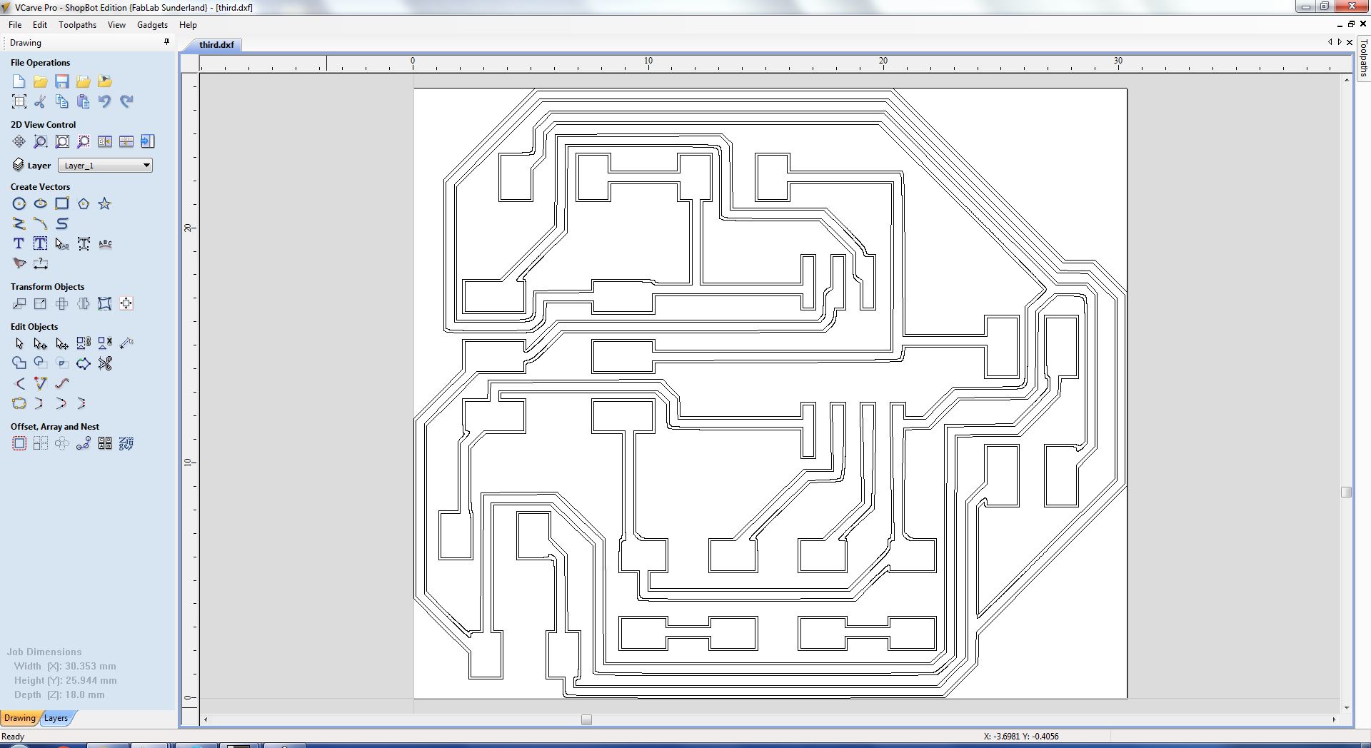
Eagle has some other export option like DXF, hence I first tried that. I can import the DXF into Vcarve and generate a tool path for it.

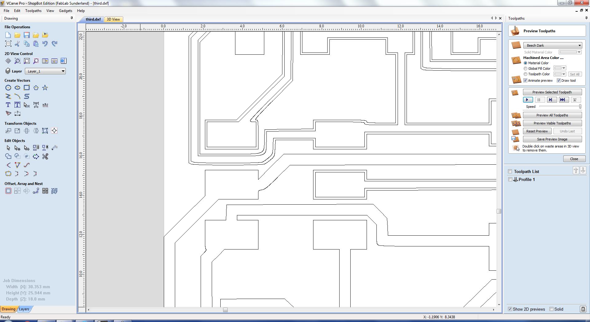
This is the exported DXF of the board, it doesn't look that promising to me. Anyway I imported the file into V carve and proceeded to generate tool paths form the file. But there was an error. There were a lot of open vectors so the software ignored most of the lines. So next I tried joining the lines. I used the join vector tools to join all the vectors, what happened next surprised me.
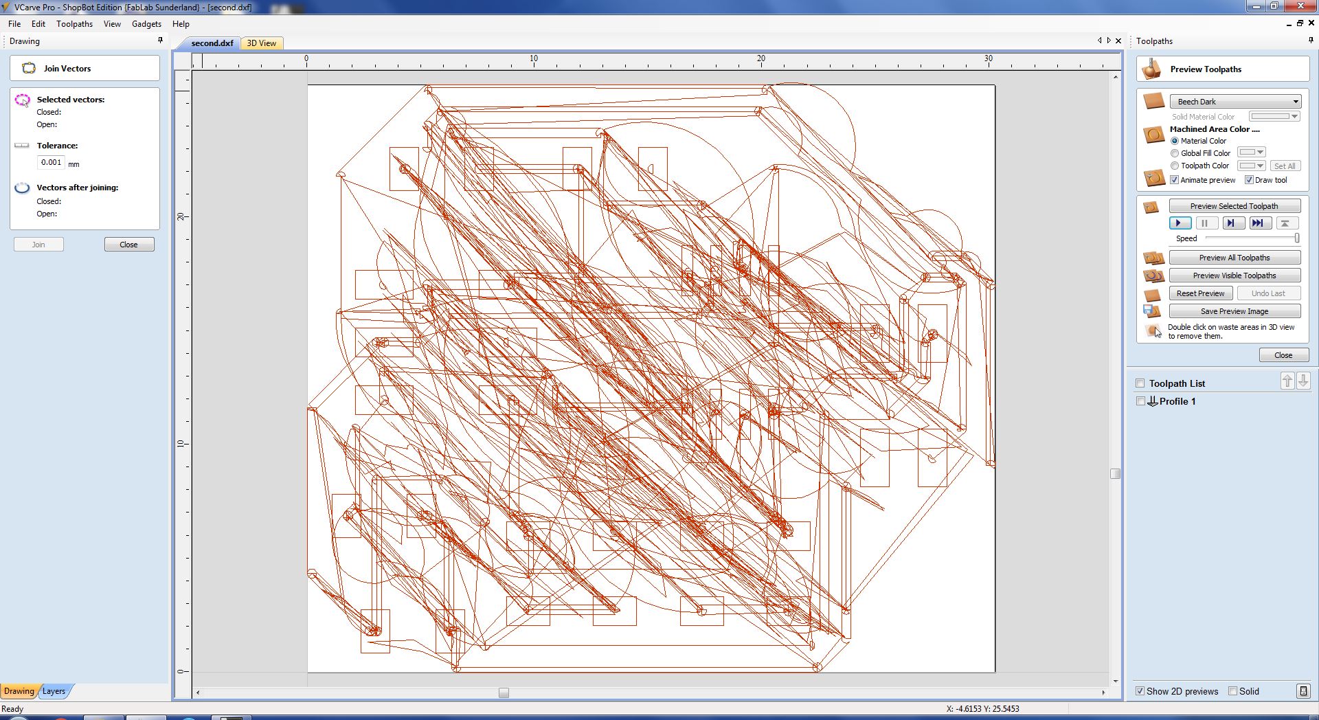
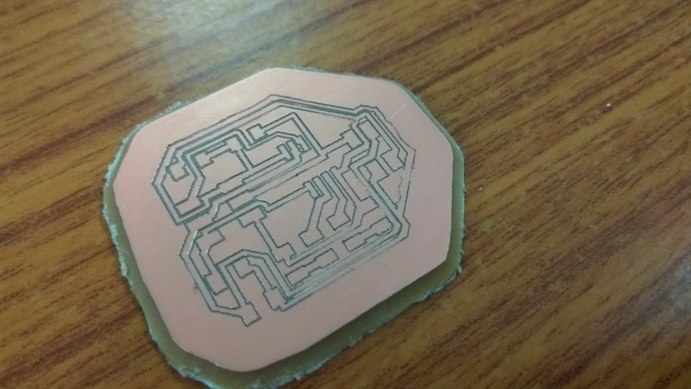
It looks like a child drawing with crayons. I though twice about putting it in my documentation. This ungodly mess is the result of join operation in Vcarve. I understood I'm not going to get anywhere with this. Time to look for a new plan.
My next plan was to convert the png file into a vector file. I imported the file into Inkscape and then Inverted it to get the traces in black. Then I traced the bitmap using edge detection to generate the vector file form the .png.
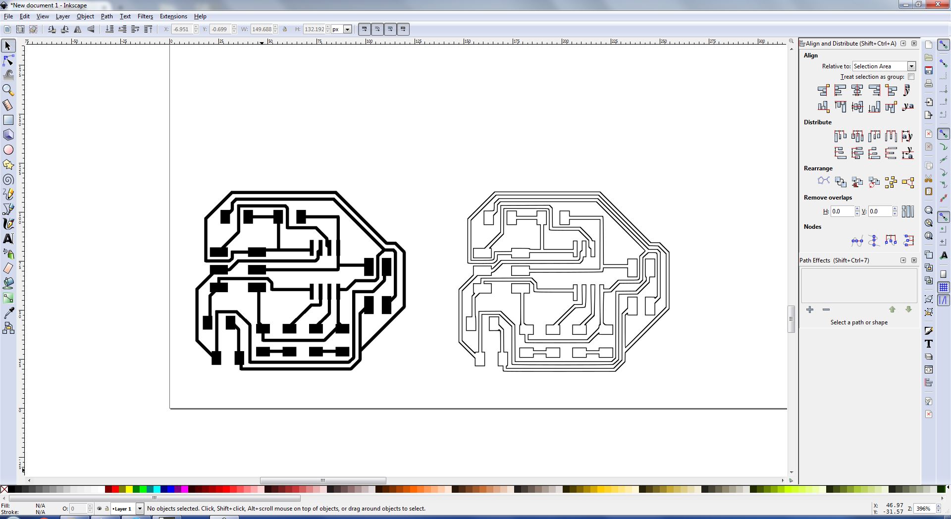
This came out good. I now have the vector files I needed. I exported the file as a DXF and opened it in Vcarve.
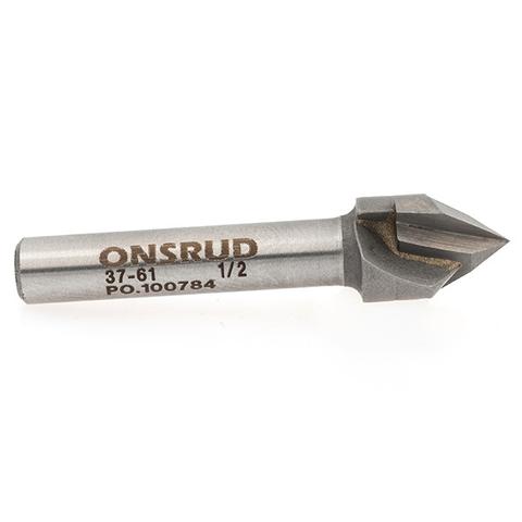
I dare not put a bit designed for modella into shopbot, hence my plan is to use the sharp edge of an engraving V-bit
There were two lines in the bit map. I gave a tool path to them with an Engraving 90 deg V-bit and set the cut depth to 0.1mm. Since I'm using a V-bit the diameter of the tool touching the work piece is really small. hence Multiple paths are not going to work.
So I began removing one of the lines from all the vectors until I was left with a single line.
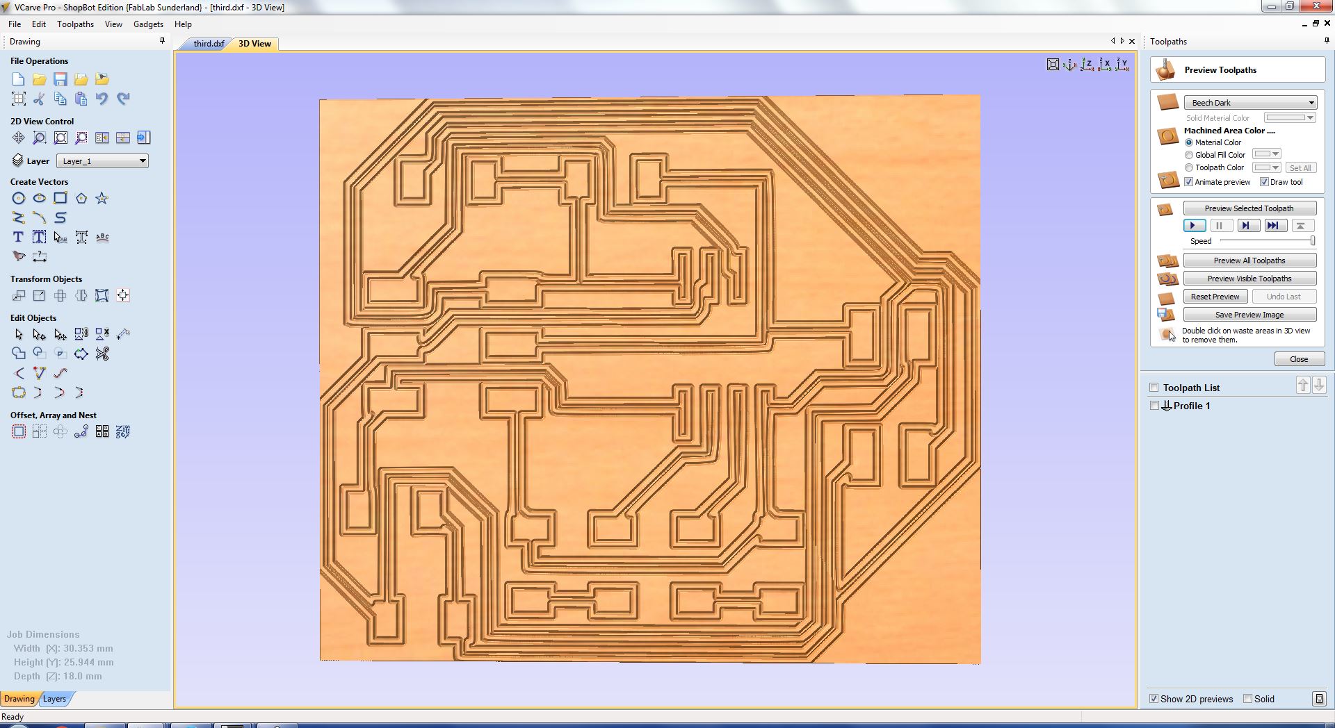
Then I gave the tool path again to see how the cut will come out.
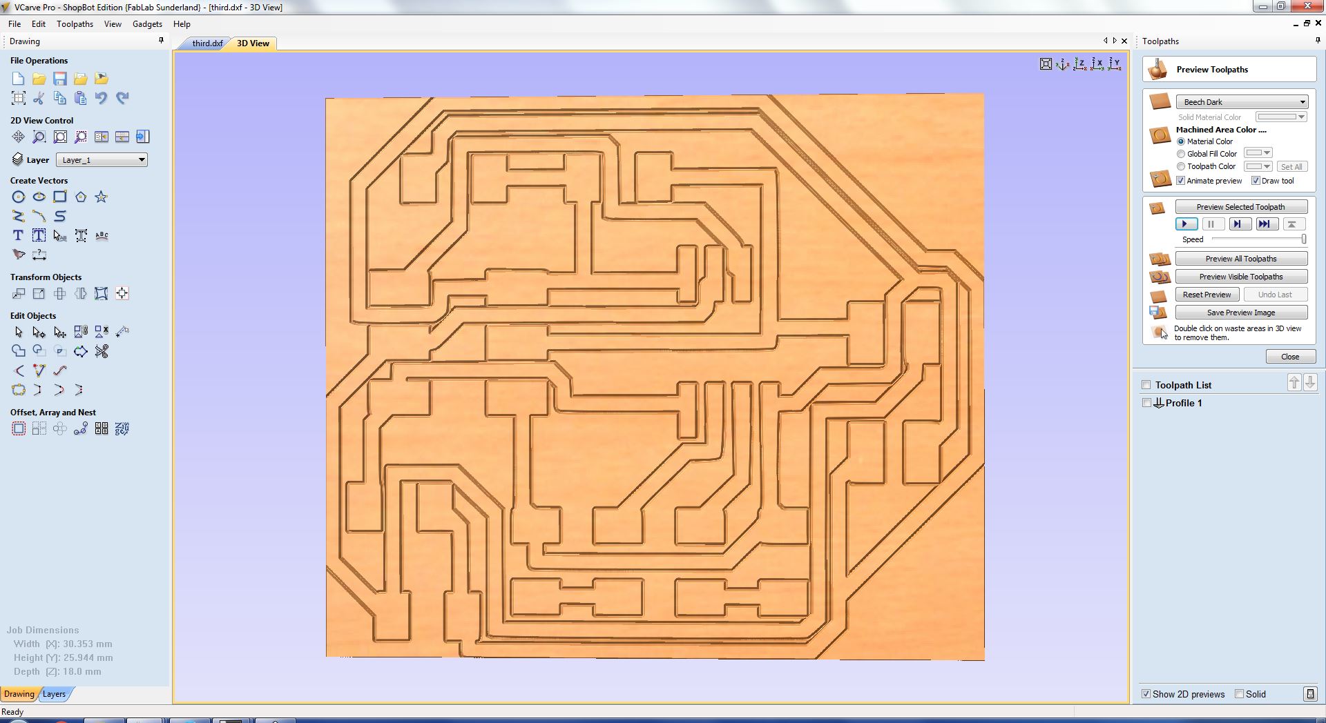
I looks good on PC, now lets try milling it so that I know how it will come out on the board.
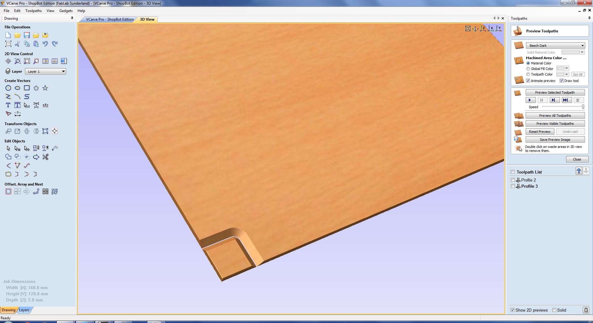
From my experince i know it is wise to first test cut a small piece first with the tool path settings, before cutting the actual product. hence I made a small rectangle in V carve to test out the tool path setting. There was two thing I wanted to know, how the traces would come out and how the cut lines would come out.
Before milling the board, you have to make sure that your bed is perfectly flat. The V-bit is very pressure sensitive, hence a slight height variation can produce unwanted results.
To avoid that I used a scrap piece of Foam board to make the base and used a 6mm bit to pocket out a 3mm hole. Now all I have to do is place my board into the hole and it would be perfectly flat.
After pocketing the hole, I fixed my board on it using double side tape. I made sure that it stuck properly on the board.
Next I changed the shopbot bit to the V-bit and set the origin. I made a mistake in setting the origin the first time, that is why there is hole on the board. The problem was that the board was only 2mm thick and it was kept inside a 3mm hole, so we can place the Z-plate on top of the board. So me and my friend tried to use the board itselt as the conductor for setting the zero. We touched the z plate with the copper and then touched the bit to see if the input was recognized, it was. It showed up on screen, hence we decided to go for it. I kept my arm on the stop button, in case if anything were to go wrong.
The spindle came down and i could see the input lit up on screen , but the bit did not stop, it punched through the board and I hit the stop immediately. I realized what had gone wrong. The program in the shopbot does not stop immediately as the input comes, it continues to put some force for sometime and then only stops. Since we were using a very sharp bit, that force was enough to push a hole through the material.
So after this, I had to set the Z-zero manually, I do this by first bringing the bit really close to the board and then, in increments of 1mm or 0.5mm I begin lowering the bit. This is a sort of aproximation, but I've had some practice with it. With that method, I was able to set the Z-zero for the bit.

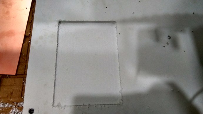
The cut came out good. There was good trace isolation and The V-bit cut through the board well. Now I was confident with cutting the board.

It looks good, time for testing the actual cut.
I loaded the program for the trace and set the X,Y position and started cutting.

This was cut with a feedrate of 40mm/s and 12000rpm, at depth of 1mm. The cut was very fast. Too fast infact. I have to reduce the feedrate for my other cuts. It took approximately a minute to cut this out. But this feedrate comes at a cost, some of the traces were too small and started to peel off.
There was some noticeable wobbling in the top trace of the board, I don't understand how it got there, might be that the board lifted off and the tool the scraped the surface. The cut was okay, but not as good as I wanted. So next i tried increasing the depth of cut to 1.2mm and reducing the feed to 30mm/s
The second cut came better, but some of the traces peeled off. The trace widths were not uniform, it might be because of the way I generated the vector file. I will have to look into that a bit more.

The second cut came better, but some of the traces peeled off. The trace widths were not uniform, it might be because of the way I generated the vector file. I will have to look into that a bit more.
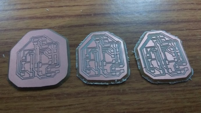
I tried one more time with a depth of 1.5mm and feedrate of 20mm/s. This time the bit removed most of the traces that I wanted. So this depth is not Ideal. Most of the traces peeled off.
Design for milling in shopbot, make the traces a bit bigger.
Ensure that the bed is perfectly level. (pocket out a small patch)
Reduce the feed rate and RPM drastically.
Use a 60deg V-bit, and make sure the V-bit is a new one (sharp).
To get some trace isolation, create two vectors and make a pocket tool path between them in Vcarve.
My method of cutting in shopbot required some refinements, but I believe with some time and effort, I can make it work. Now I had two option, One is to redesign my board and cut in shopbot or just mill my existing board in modella. I went with the latter. I will experiment later when I get some time.
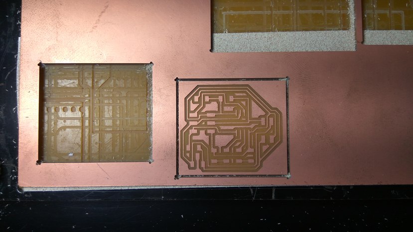
Now i imported the same file into fab modules to mill the board in modella. I used a 1/64" endmill for cutting the trace.
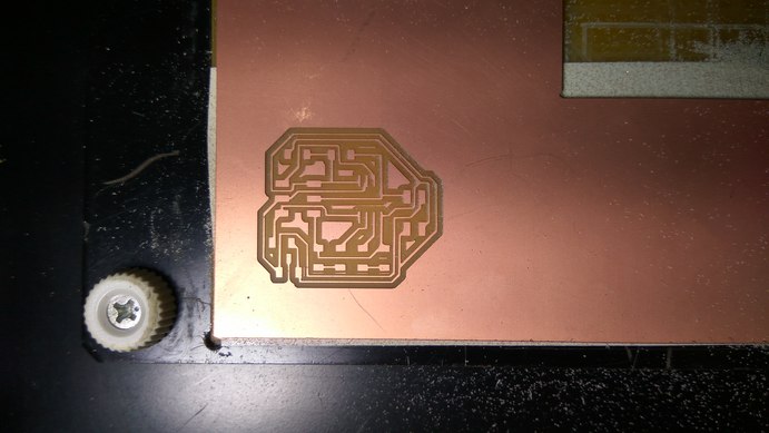
The cut tool about 14mins. but in the end it came out really good. The trace were intact and there was good isolation.
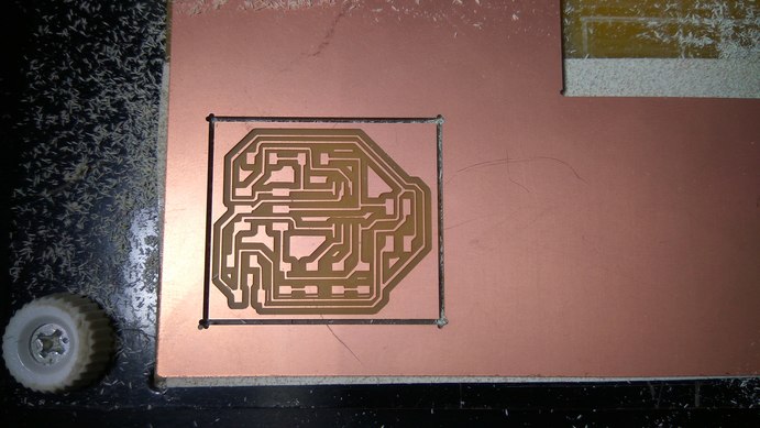
The cut line for the board was cut with a 1/32" end mill with default settings on fabmodules.
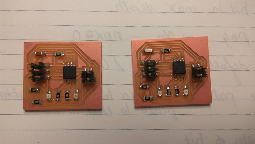
I collected all the components I needed for making the board and proceeded to solder them on to the board starting with the MCU
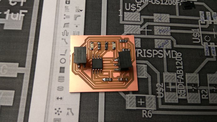
The soldering went good, I was able to solder all the components without any problems, I have wrote detailed steps on how to solder SMD components in my Electronics production lab.

I wrote a simple blink program to make sure that the board was working properly and the LEDs lit up.
The next step is to network the board with satsha kit.
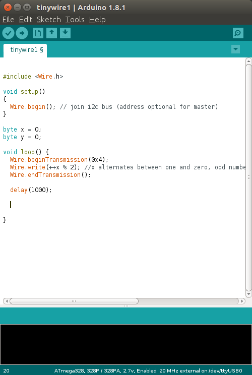
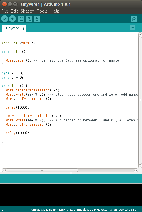
This is the arduino code I wrote for the Master(satsha kit). The code in arduino is simple. You first have to install a library called Wire.h, which you can find in git hub. Download the package and extract it to the libraries folder of the arduino IDE. Once its installed, you can use the wire.h in your code.
In the first step, we include the library wire.h. Then we give the command Wire.begin() This will start the I2C bus. The next command wire.beginTransmission(0x4) Will talk to the node with the address 0x4. Then we use the command wire.write() to write the value alternating between "1" and "0". Then we end the transmission.
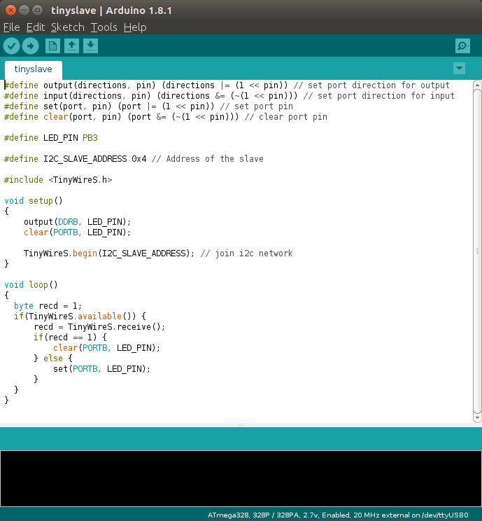
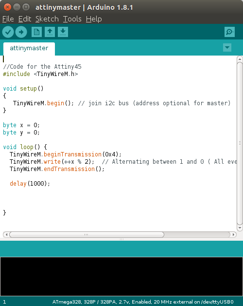
The wire.h library does not work with Attiny seires, so we need to install an additional library to the IDE. It is called Tinywire There are two versions of this TinyWireM.h for the Master and TinyWires.h for the slave. You can download both of them from Github.
After installing the Tinywire library, you can start writing the program for the Attiny. The arduino code for the node has a Slave address which is defined, in this case 0x4. To join the I2C network with our predefined address, we use the function TinyWireS.begin(). Then we put the condition if TinyWireS.available() Then read the incoming data and Turn the LED ON/OFF.
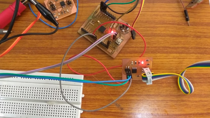
First I used an Arduino Uno to check the code to see it its working. I connected the SDA, SCL lines and powered the two boards.
The code works fine. The LED on my board lit up once every second. Now it is time to try the code with satshakit.
I connected the circuit in the same way as in Arduino Uno. The SDA, SCL lines were connected together and i used a breadboard to power both the boards. But then nothing happened. I double checked all the connection to see if there was any loose contact.
But the program was not working correctly. I wanted to see where the fault was, so I used an oscilloscope to check what was being generated. But a strange thing that happened was that, Sometimes the LED would turn on when I touch it with the oscilloscope probe and then stay ON. I did not know what was happening.
This was strange, somehow touching the connections on my board with the probe would trigger the LED to turn ON. I connected the probe to the SCL and SDA lines to see what output was being generated.
This is the SCL line with the satsha board set to run on the external 20Mhz resonator. I could see the clock pulse that is sent to the node. I did not know if using a different clock frequency on my Master and slave would result in communication error, so I played with a couple of clock settings trying it at different frequencies to see if the code would work.
The SDA lines show the device pulling down the line to communicate, so I know communication is happening, but the code was not working.
I got this reading in the middle of my debugging process, I honestly don't know what it is, so I recorded the output to see if I know find out what was going on there.
Lastly I tried running both the master and the slave at 1Mhz internal clock. I wanted to know if the code was not working because of a clock mismatch.
This was the SCl reading at 1Mhz, there seems to be a lot of noise in the signal.
This is the SDA reading at 1Mhz, The wave is not as smooth as before, there seems to be a lot of noise when I shift to the 1Mhz frequency. I don't yet understand where it came from.
What ever I tried, I could not get the Satsha kit to communicate with my node. So after many days of debugging and not finding a solution to the problem, I switched to making a second node. Our assignment was to network two micro-controllers and make them communicate with each other. So I had an idea to make a second node, interconnect them together and make them communicate between each other. My instructor told me that I have to communicate to multiple nodes using addressing.
So I began making the same node I designed earlier.
Update: I'm writing this after my final project presentation, I realized now why I was facing problems with satshakit. In my assignment I used I2C protocol, which requires the use of SCL and SDA pins of the MCU. I followed the diagram given in the satshakit github page to connect my circuit. I realized while working on my final project that there is a slight error on the diagram. The SCL and SDA lines are switched, I found this out while referring to the Atmega 328p Datasheet. That is why my circuit was not working, the SCL and SDA lines where connected in reverse.
Finally got the satsha kit working with I2C. The problem was solved when I connected the SDA and SCL lines properly and the two boards are running at 1Mhz internal.
The board was milled on modella using the same settings and end mill.
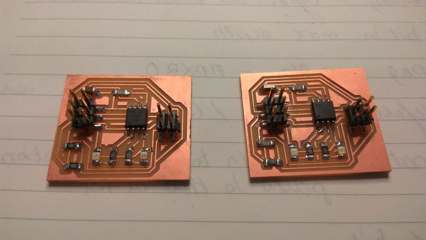
Here is the final stuffed board ready for testing.

I'm getting tired of plugging in and removing a heck lot of jumper cables, So to ease my burden I made a serial bus cable to connect my boards together.
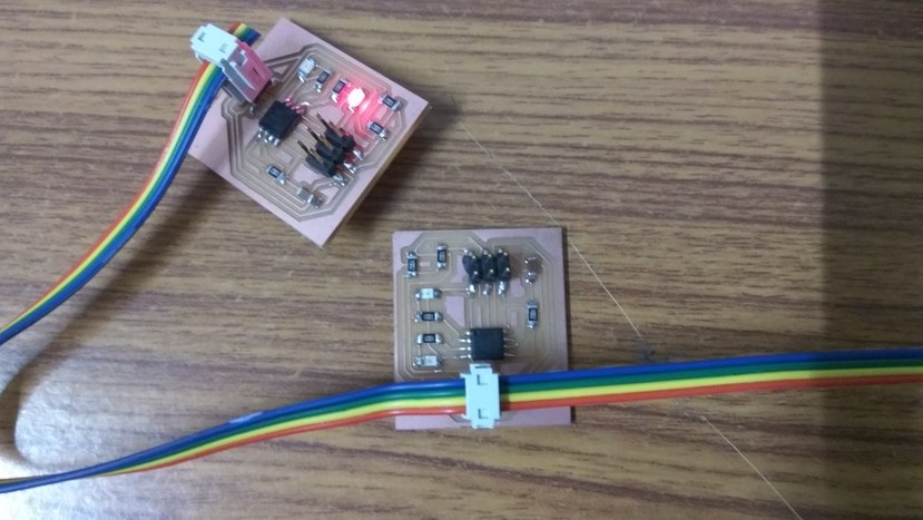
This helped a lot in speeding up the programming phase.
This was just out of curiosity, i gave the same address to both and wanted to see how the communication would happen. They both responded at the same time.
The arduino code for the master is almost same except of the addition of a small snippet to address the second node.
I have given two different addresses to the two nodes, One is '0x3' and '0x4'. So now i have two wire transmissions, one for the node 0x3 and the other for the node 0x4. The nodes will respond to the communication, only if their addresses are called.
The arduino code for the slave is largely similar, except for the fact that two nodes have two different addresses. One being 0x4 and the other 0x3. They we burned into the MCU of their respective nodes.
The code worked beautifully. I can now talk to two different nodes on the same network just by calling out their address. The code is written in so that when the nodes receive an input from the master, it Lights up the LED and stays On for 1 second. That is why you can see the in between both LEDs are on.
There was one last thing I wanted to try, till now I've been using a Arduino as the master and two nodes as the slave, I wanted to see if I could make one of the node boards as the master.
The problem was that the wire.h library will not work with an Attiny series, so I had to find a new way.
I searched online for a way to do this, until I found the TinyWireM.h library. Now I understood how to write the code for the master. I added the library and changed all the wire functions to tinywire functions and burned the code into one of the nodes.
The code was uploaded into the Attiny and successfully. Now for the slave code.
There isn't much change necessary for the slave code, just make sure that the address you give to the salve is the same as the one in the master.
This code works well. Communication is happening, but one thing I noticed is that the LEDs were blinking much faster than before. i had given a one second delay, which does not seem to be working. I'll have to do some further testing to find out what is happening.
Overall, this has been my most toughest week since the academy. I was clueless about what to do. I have to thank a lot of my friends for helping me thins week. I'm glad I took I2C as this weeks assignment, now I have an idea of what it is and I can implement it in the future.
rahulsrajan.com
rahulsrajan01@gmail.com
Trivandrum, Kerala ,
India.

Technopark, Kerala, India

