"
Sixth Assignment
PCB Design
This Excercise was about:-
1-redrawing the echo hello-world board.
2-add (at least) a button and LED (with current-limiting resistor)
3-checking the design rules, making the PCB, and test it
4- a)extra credit: simulating its operation
4- b)extra credit: measure its operation
EAGLE
In this assignment I've used Eagle software (Easily Applicable Graphical Layout Editor), I chose this software as it's user friendly and because of its freeware license and rich availability of component libraries on the web.
I downloaded it from Here

Eagle Tutorial by Jeremy Blum
One of the best tutorials I've found on the Internet was Jeremy Blum's Eagle tutorial which consists of 3 videos.
Tutorial 1 for Eagle:Schematic Design
Tutorial 2 for Eagle:PCB Layout
Tutorial 1 for Eagle:CAM output and DFM

Starting a New Project
I decided not to download the ready schematic and project from the internet to be able to learn more on how to start a PCB project.
the first step to make a new project.
then make a new schematic.
note that you have to keep both the schematic and the board layout open and not to close any one of them as closing one view while the other view is open (and making edits) will break the link between the two.
.png)
Adding The Componets to The Schematic
The components I had to put into the schematic were as in the screenshot
.png)
Using Libraries
One of the most important pros of the Eagle software is the various libraries where you can find almost any component you want.
I used Neil Gershenfeld's Library and Fab library library
(you can download them from here)
fab.lbr
ng.lbr
then you can use them and add components from them as shown in the pictures.
.png)
.png)
.png)
After Adding Some Components
After adding the components in the previous step here it looked.
there is two methods to wire the components together:-
1- using Net order
2-Naming the wires the same name without connecting them (we use this command not to get it so messy)
.png)
After Adding all the components and wiring them
It looked like this, note that the wires which have same name are connected.
when you are trying to name two wires the same name you will get a message like "Connect A&B"
select Yes to accept connecting them.
 - copy.png)
ERC Check
We have to make ERC (Electrical Rule Check) to make sure that there is no errors in the schematic of our board.
these errors were acceptable to me; because it's not that important to assign a value to a button, and I really don't need the RTS neither the CTS pins.
.png)
Switching to board layout
After making sure that I don't have errors in my schematic design, I need to switch to board layout to design the traces and the layout of the PCB.
You will find the added components with their real footprients are added to the BRD layout and looks somehow messy like this.
(Actually I arranged them a little in this screenshot)
.png)
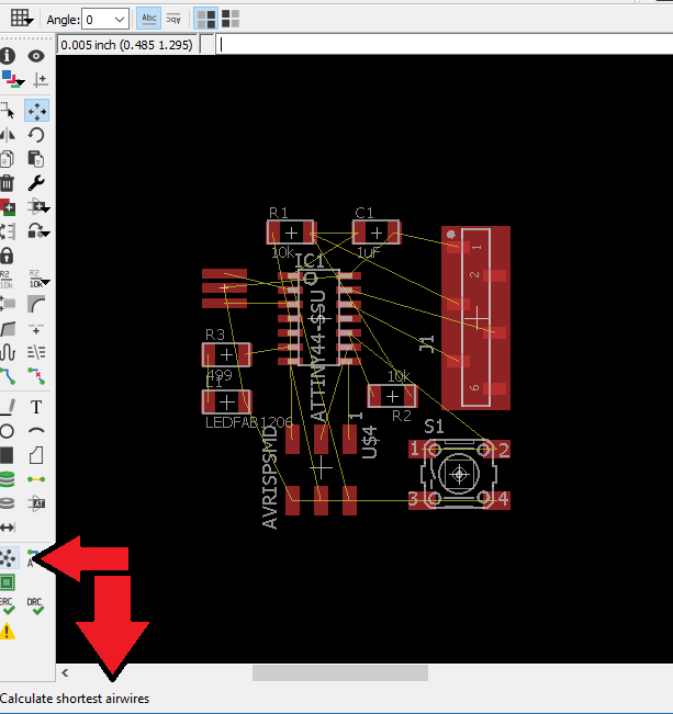
Select the shortest route
After arranging your components in the board layout you can use this option of selecting shortest routes to make it easier for you to make AutoRoute or manual route.
.png)
Autoroute
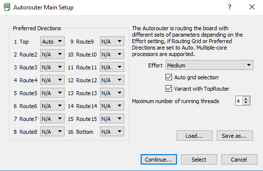
After this step you can easily make Autoroute, in my case I was using only one layer pcb that's why I selected all the layers as N/A and only the top layer was selected as Automatic.
.png)
Manual route
After autrouting you might find some traces which are not connected yet, so you can try to make it by yourself manually from this option
.png)
Adding Jumpers
After adding the traces I hade only one connection remained, that's why I added a jumper.
the jumper in surface mount PCBs is a 0Ohm Resistor.
.png)
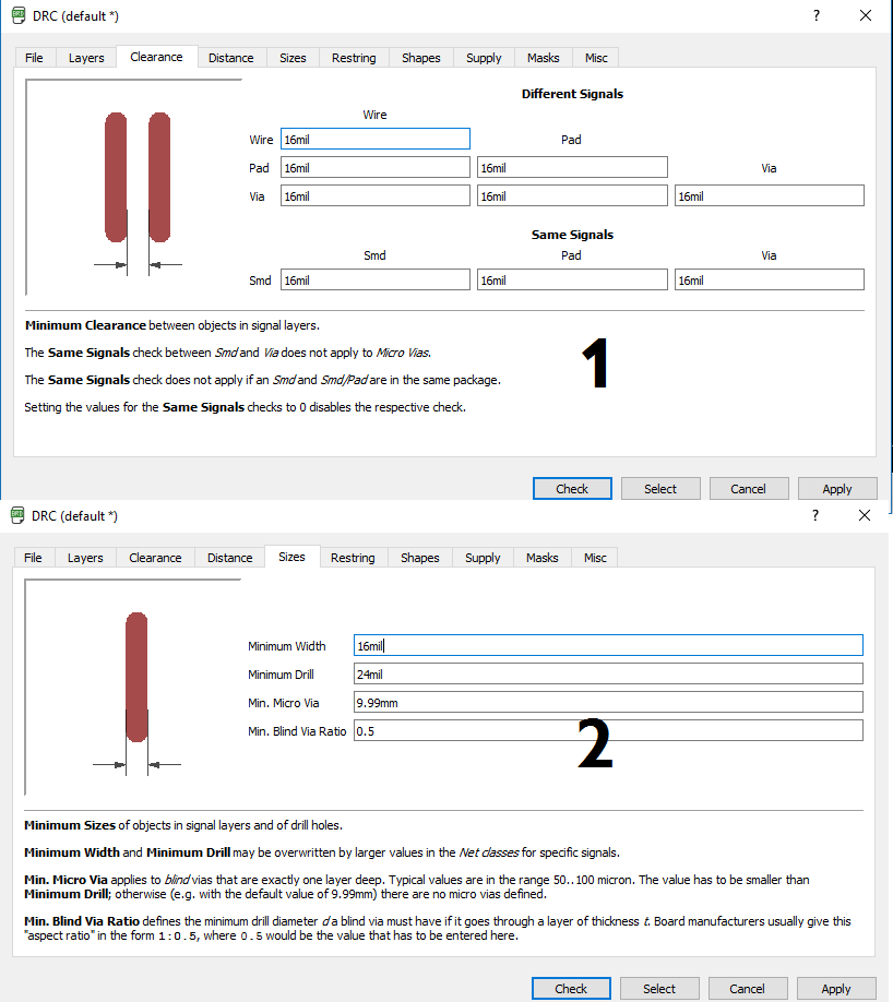
DRC (Design Rule Check)
Before sending this PCB to be milled I have to check that there's no error's in the design.
Luckily in this board I had no error in the DRC.
after selecting DRC from the bottom left you have to set the parameters you want to check, the most important parameters are the clearance to be sure that the end mill will have enough space to make the traces.
I selected 18 mil because the endmill was 16 mill. you can use 16 but I wanted to be more sure that the PCB will be good, and the machine wasn't well calibrated.
.png)
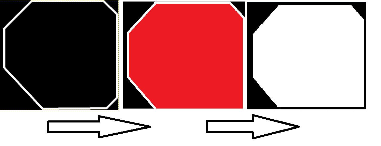
Drawing the Outline
you can draw your unique outline by selecting the order (Draw) and select any color other than the one used in traces; as it will be exported in another file.
.png)
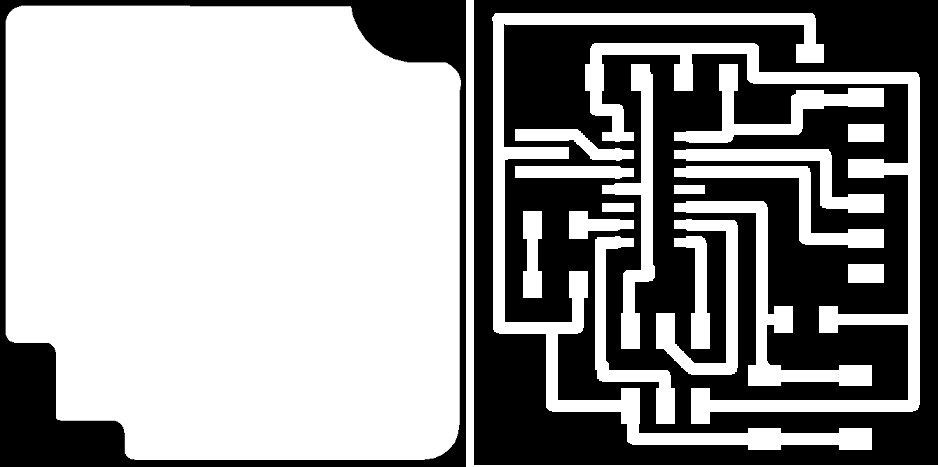
Exporting the Traces
select viewing only the top layer as shown in the Picture then export as IMAGE monochrome and select dpi 500 (recommended).
by doing the same with the outline by slecting the layer (Dimensions 20) and exporting it you will have both the PCB traces and the outline to be machined like demonstrated in electronics production assignment (check the assignments webpage).
.png)
Just one last step
you have to edit the exported outline by paint or Gimp to make it like this one in the picture.
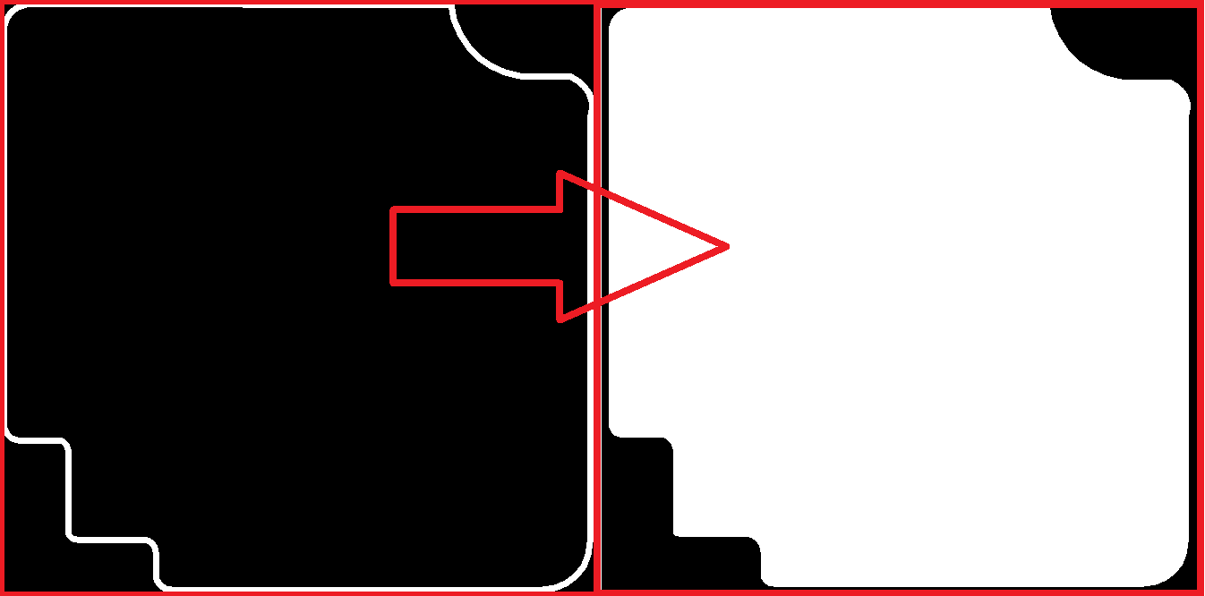
TaDaaaaa
here are the two files that should be sent to the PCB milling machine.
NEEDS CORRECTION
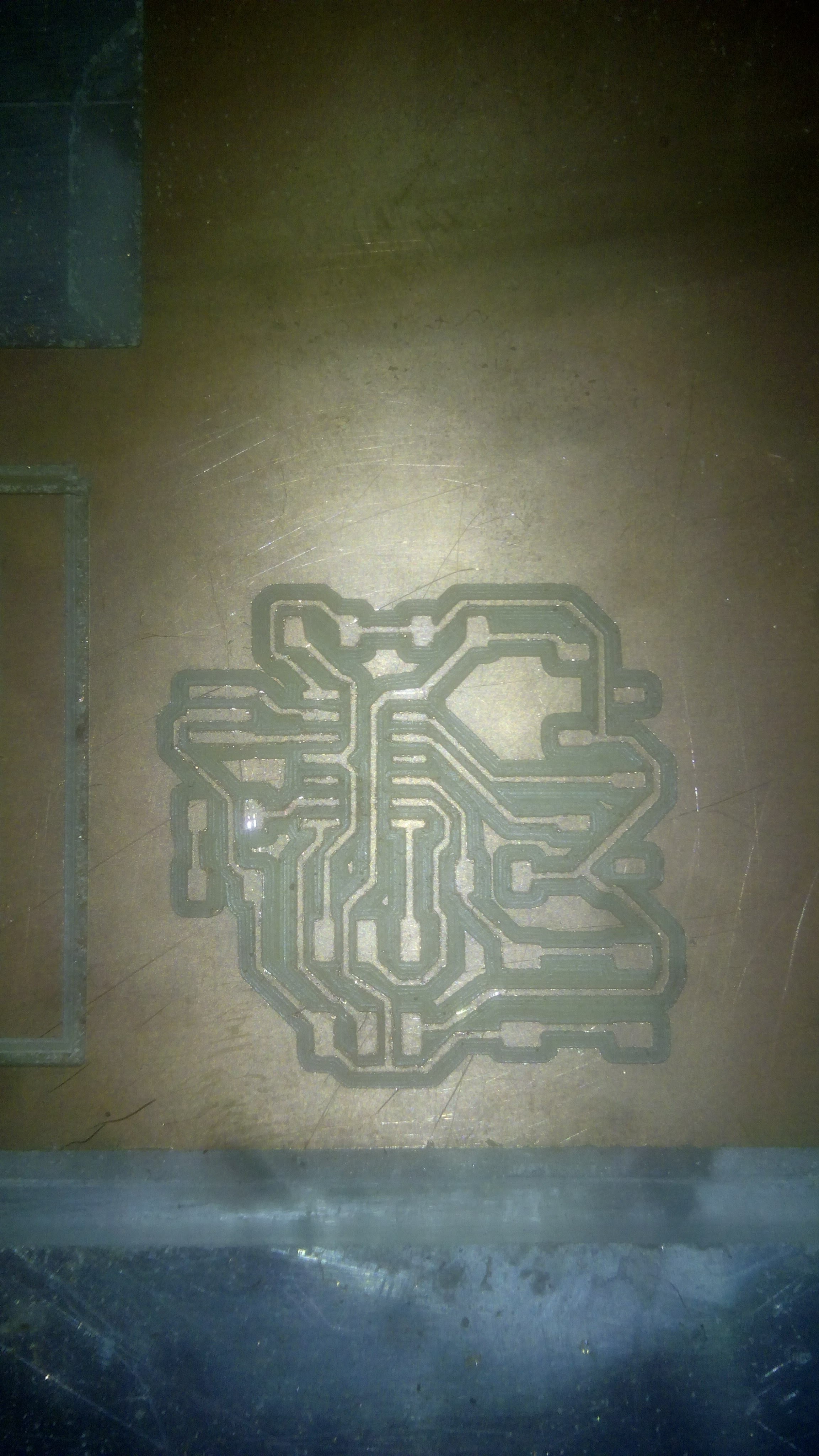
the PCB wasn't of the best quality because I've used a broken endmill to make the PCB to get the assignment done that's why I've made the traces so thick.
after making sure it's working and after getting new end mills I tried to make it again with a better quality.
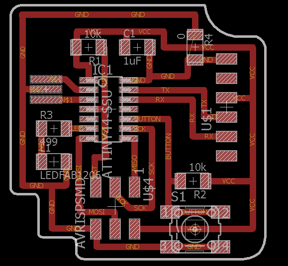
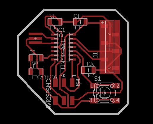
Redesigning the Board layout
the errors were in the BRD layout that I didn't make the DRC check right, I've decided to redo the board layout with the same schematic (it was working well).
Editing the schematic
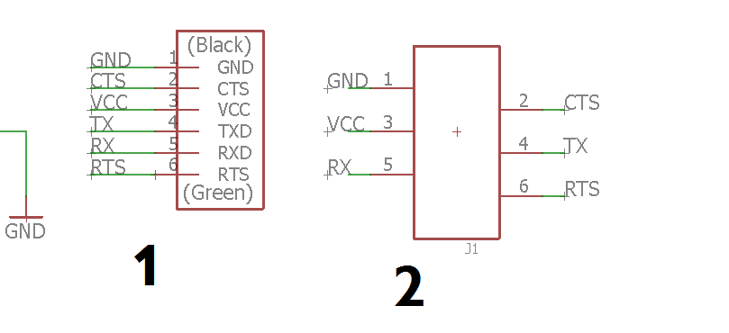
the first step was changing the FTDI headers to the ones in the lab.
I also used another library for the pin headers of the FTDI because In the lab we are using another package than the regular one used in FAB library.
EAGLE-BOARD-TO-BOARD_CONNECTORS-rev16c.lbr when adding these pins from the library search for "61000618221".
these pin headers couldn't be replaced.
After arranging the components in the board layout
This is how it looked before connecting the components in the board layout and after calculating the shortest air wires.
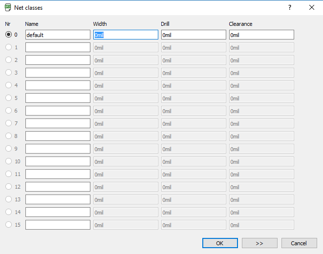
Some setup to make autoroute
to make autoroute with specific properties you have to make your inputs in the Netclasses (in edit menu).
I've selected 16 mil for clearance (because I am using 1/64 endmill)
And 16 for trace width (it can be 10 and still safe)
In the case of making the PCB surface mount components I have nothing to do with the drill dimensions.
Autoroute
I selected only top layer and medium effort (it takes less time than "HIGH" and better quality than "LOW".
and NA for all the other routes.
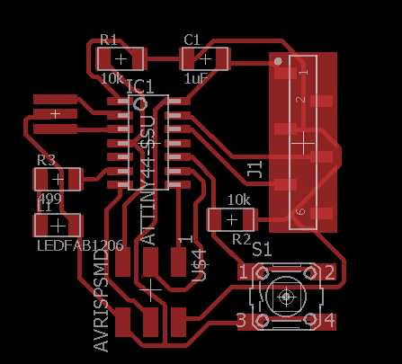
After Autoroute
this is the accomplished traces done by the autoroute.
Making The outline
It was made as described in the previous steps in making the first PCB.
DRC (Design Rule Check)
In case of making the PCB by the autorouter and you are sure that you've selected the dimensions correctly in the Net Classes step , you don't have to make the DRC,
but just to make sure that every thing is ok.
In my circuit the critical things that we want to check is the clearance and the dimensions.
the clearances have to be more than 16 mil as I am using 1/64 endmill.
and I selected the width to be 16 mill. (more safe and not too big)
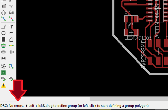
DRC Result
After Pressing Check you will see either the errors or a message of "no errors" in the bottom.
editing the exported PNGs
all I want to edit on the PNGs is the colors of the layout.
I use Fill with colours from tools in paint (the bucket icon).
Resize in fab modules
you can resize the png in fab modules if it have any errors, just press resize and enter the actual dimensions.(it rarely happens)
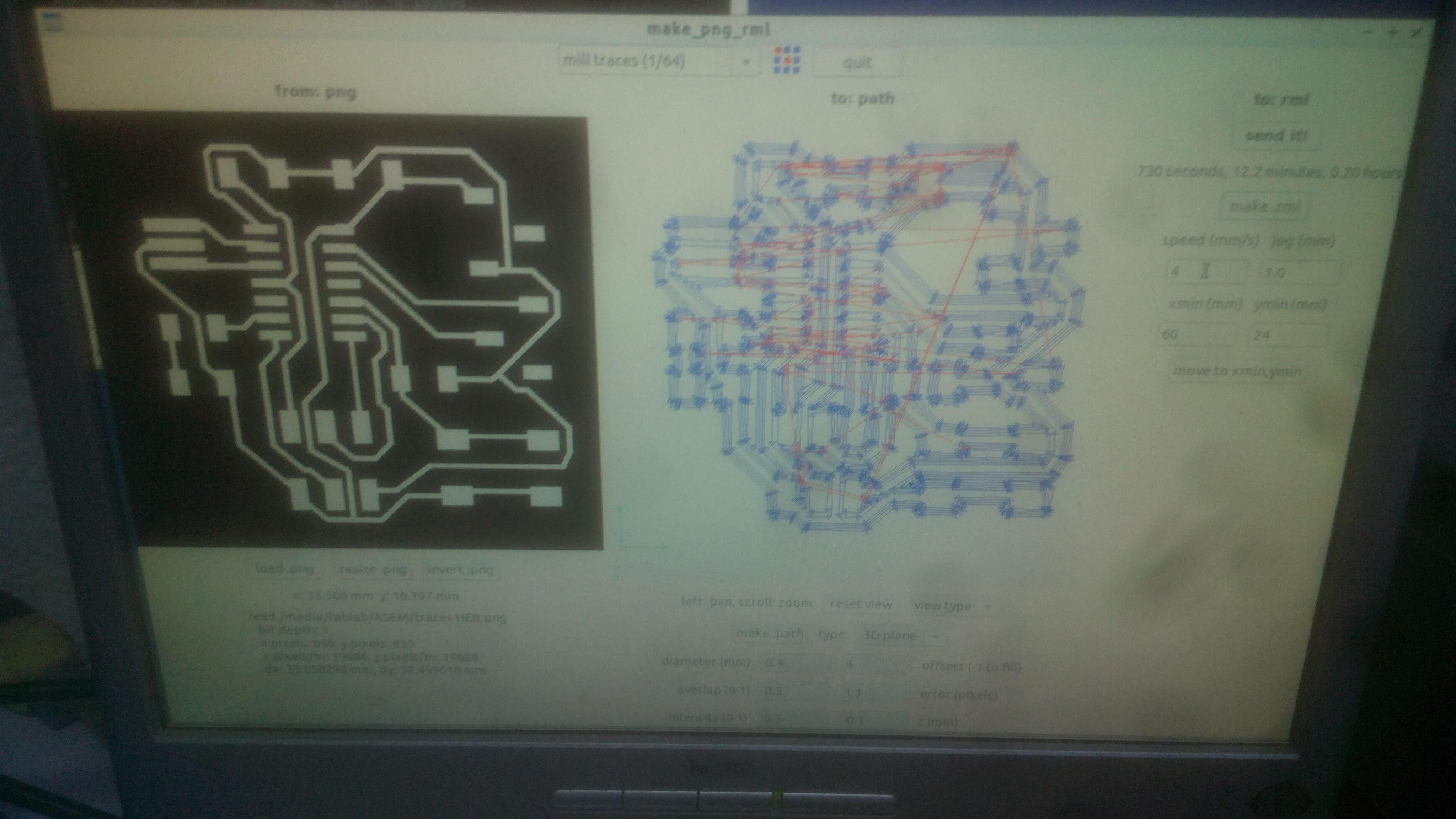
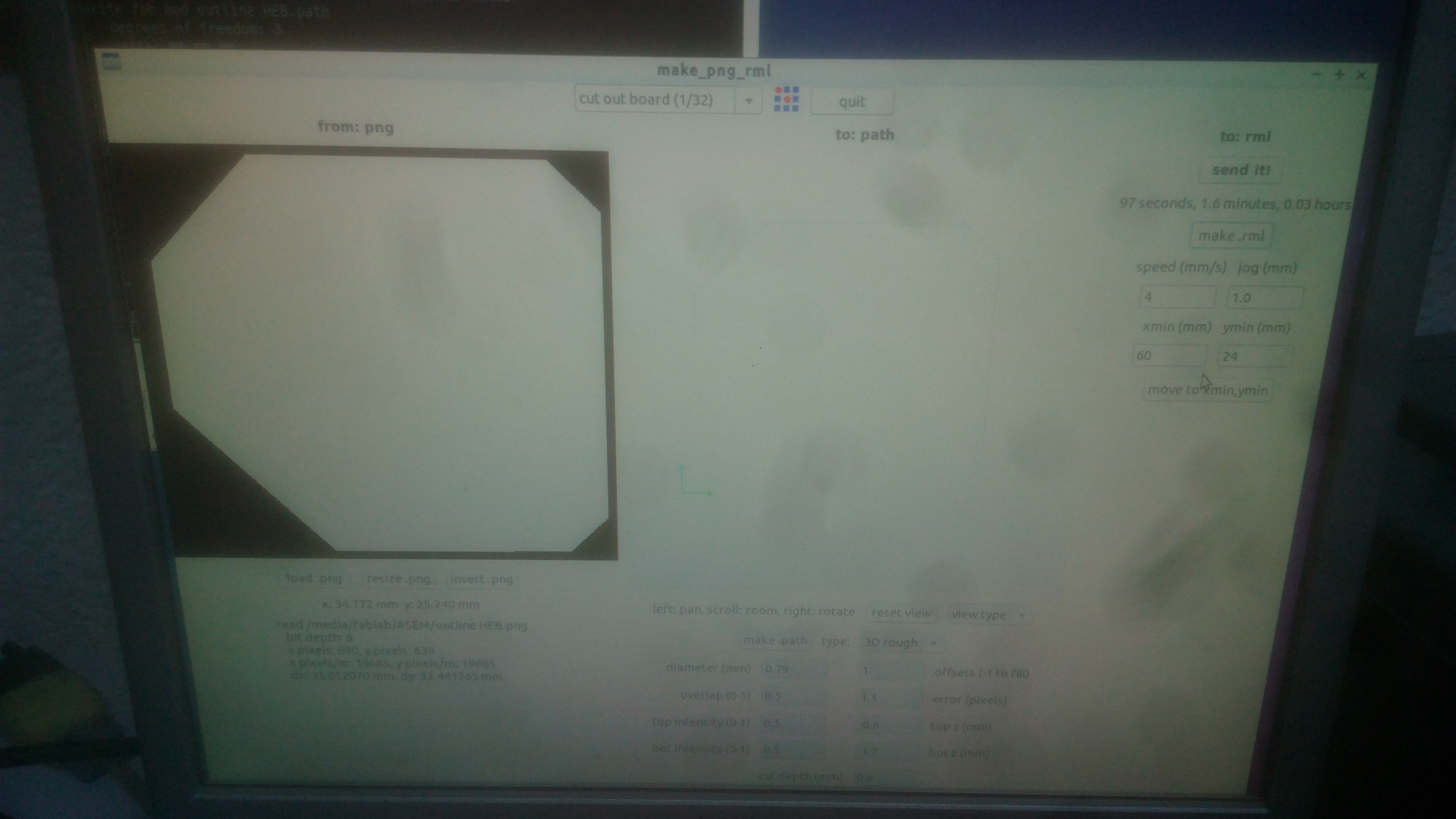
Preparing the file for the milling
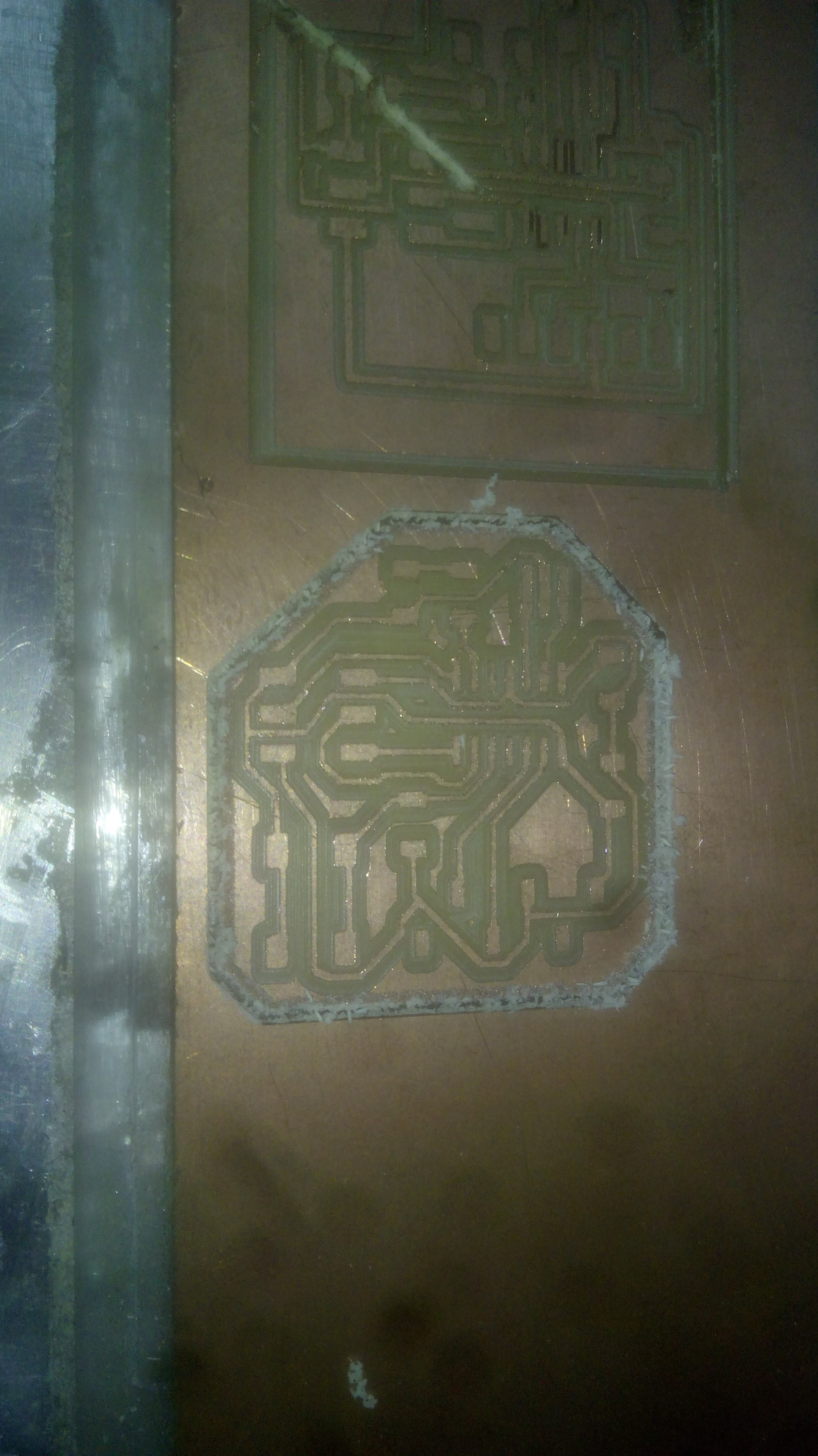
after milling
Preparing the file for the cutting out board
after cutting out board
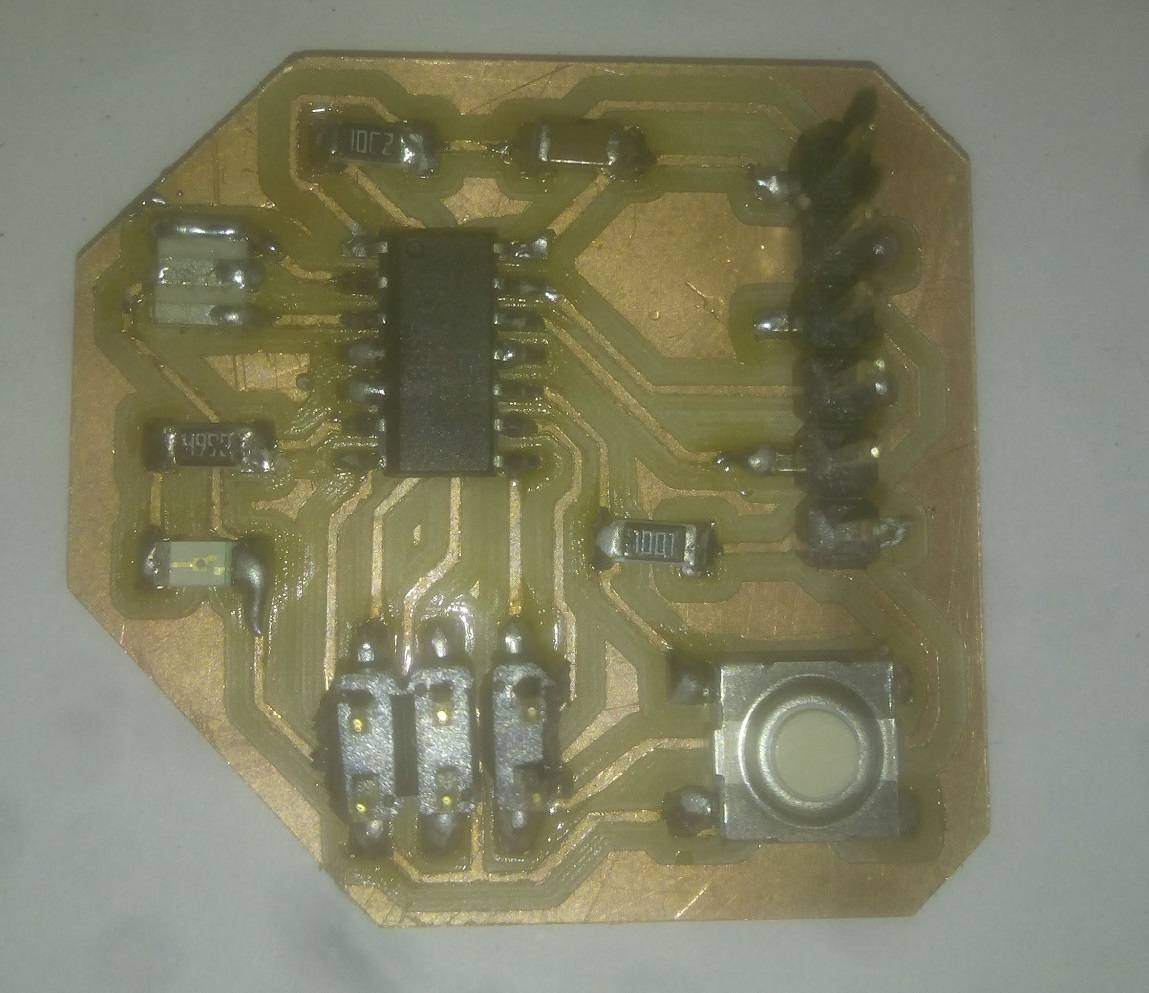
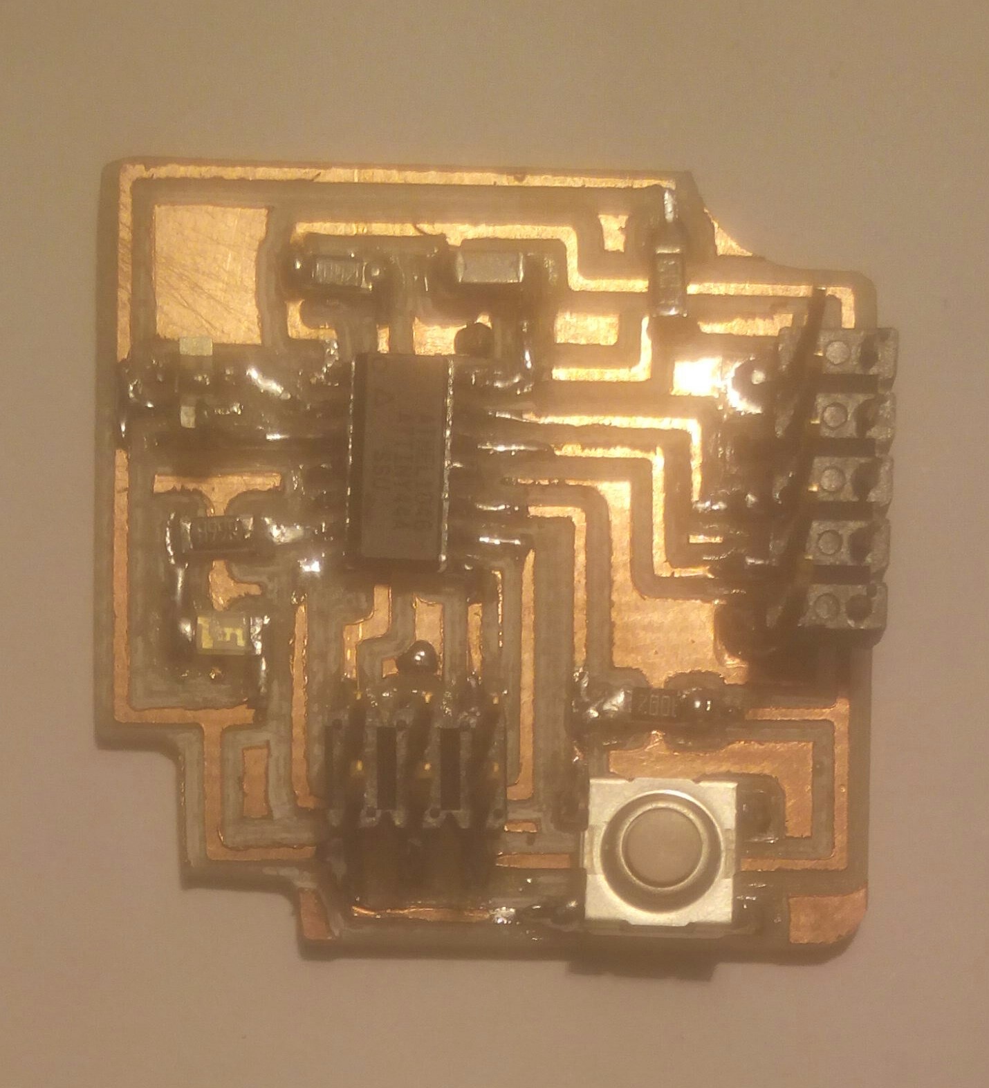
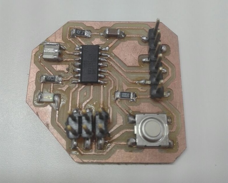
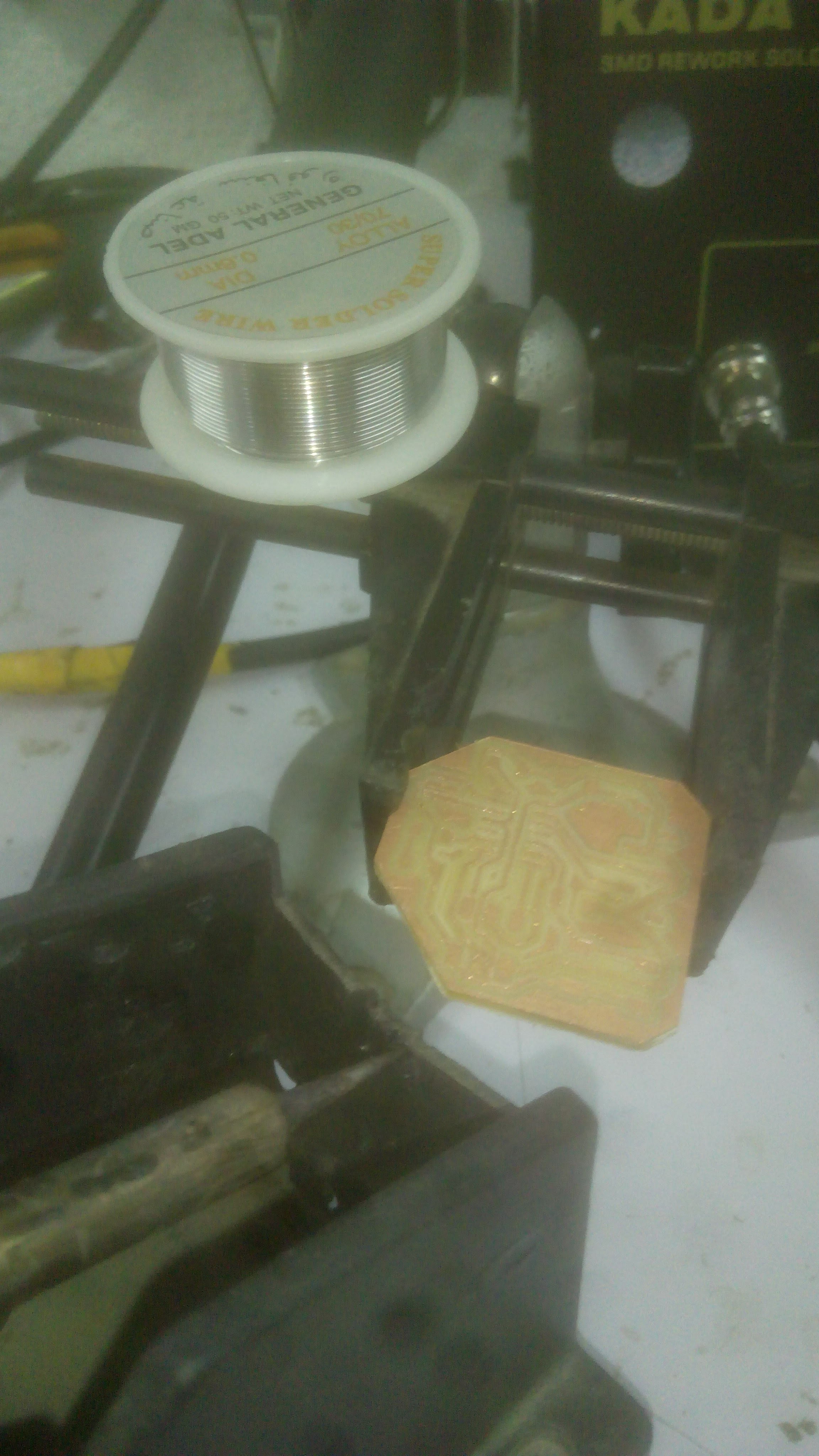
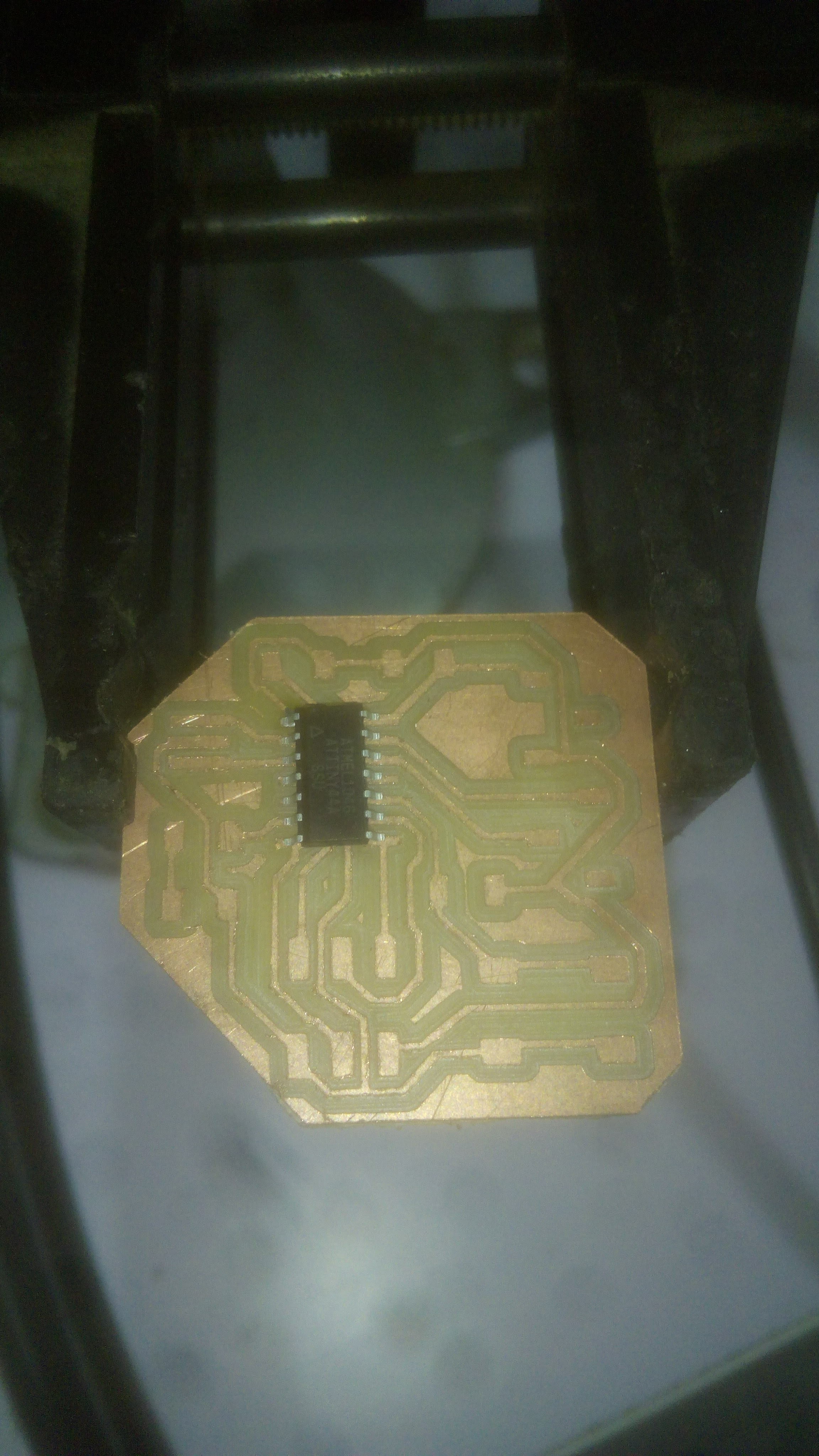
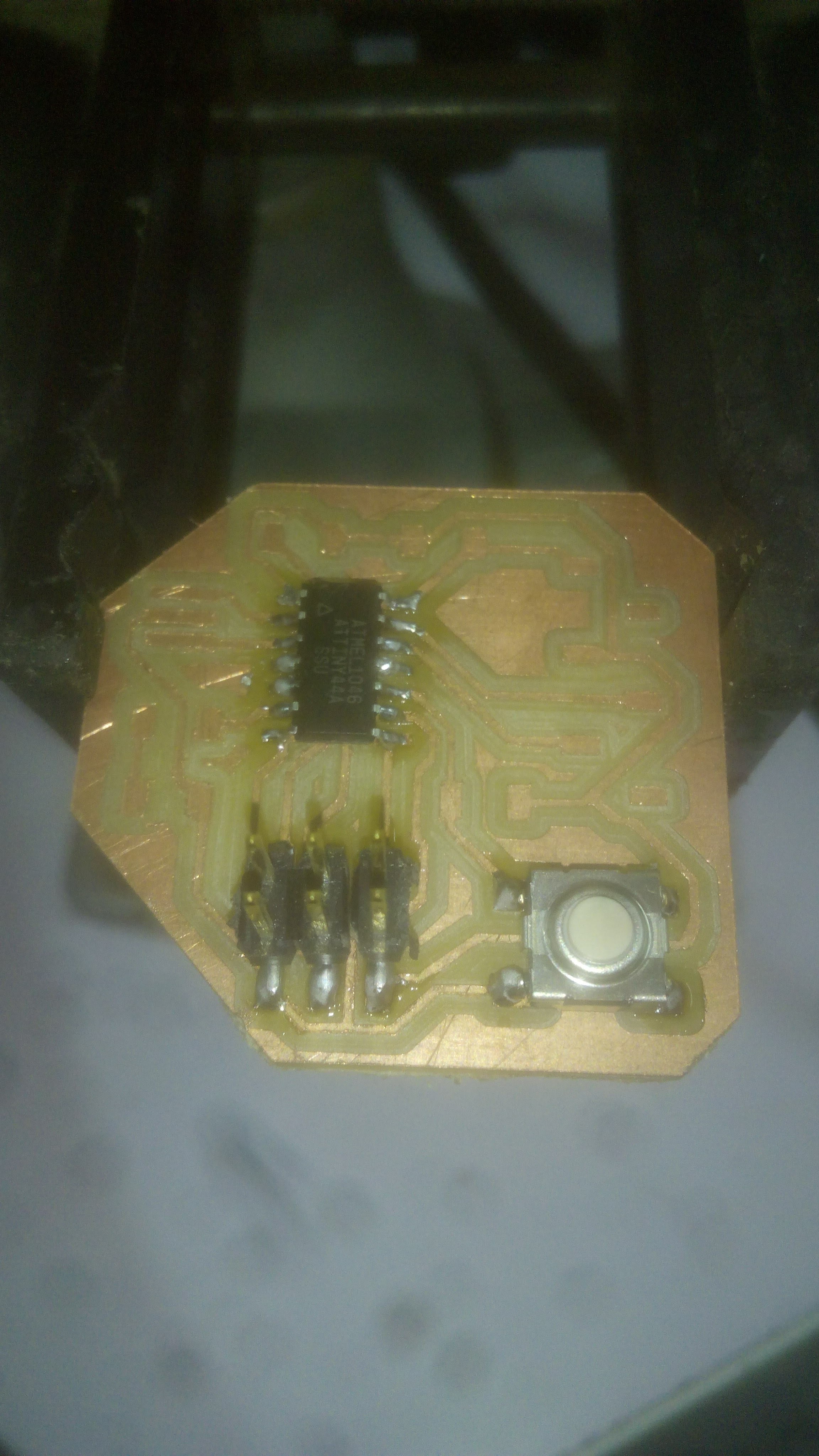
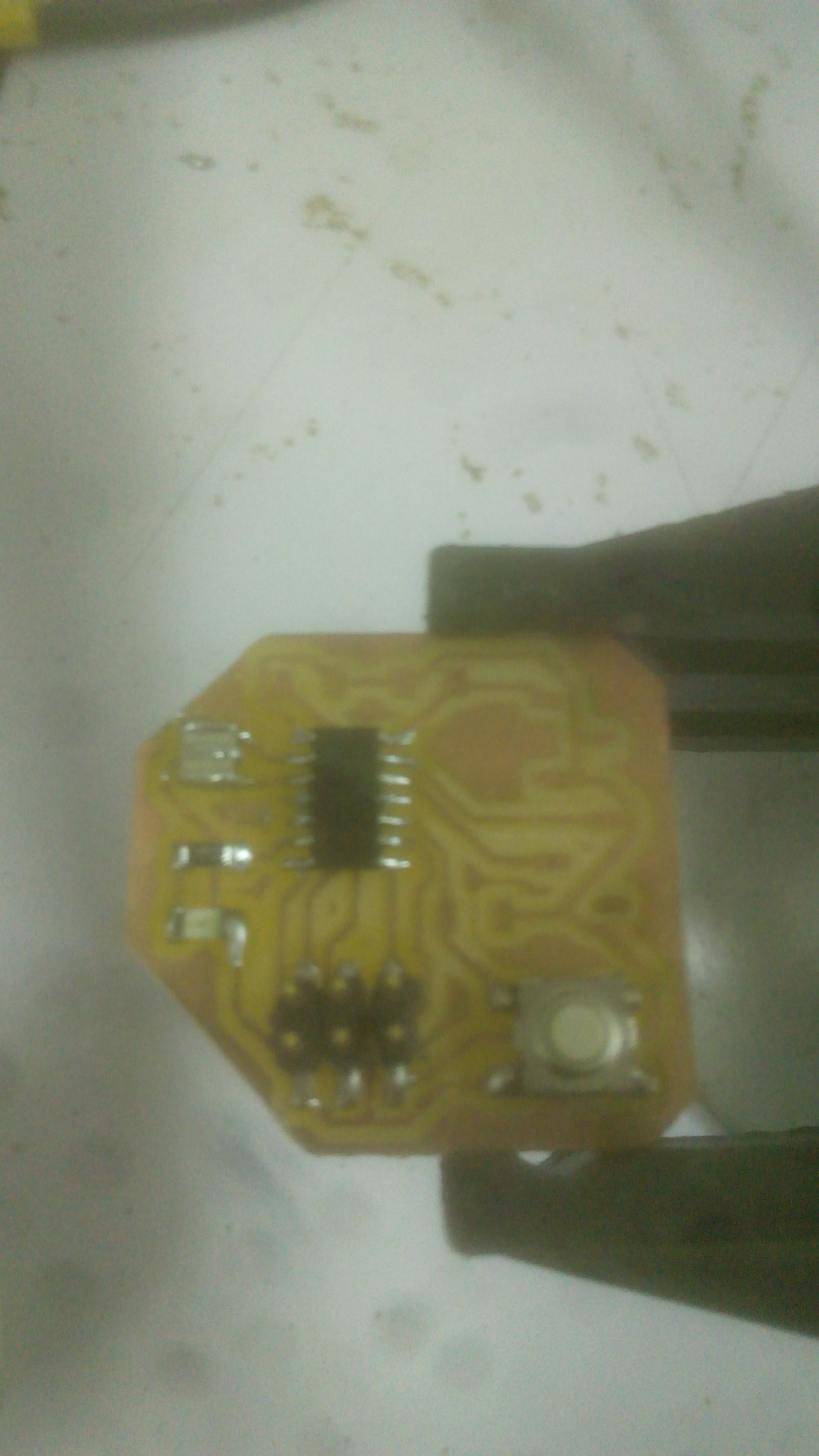
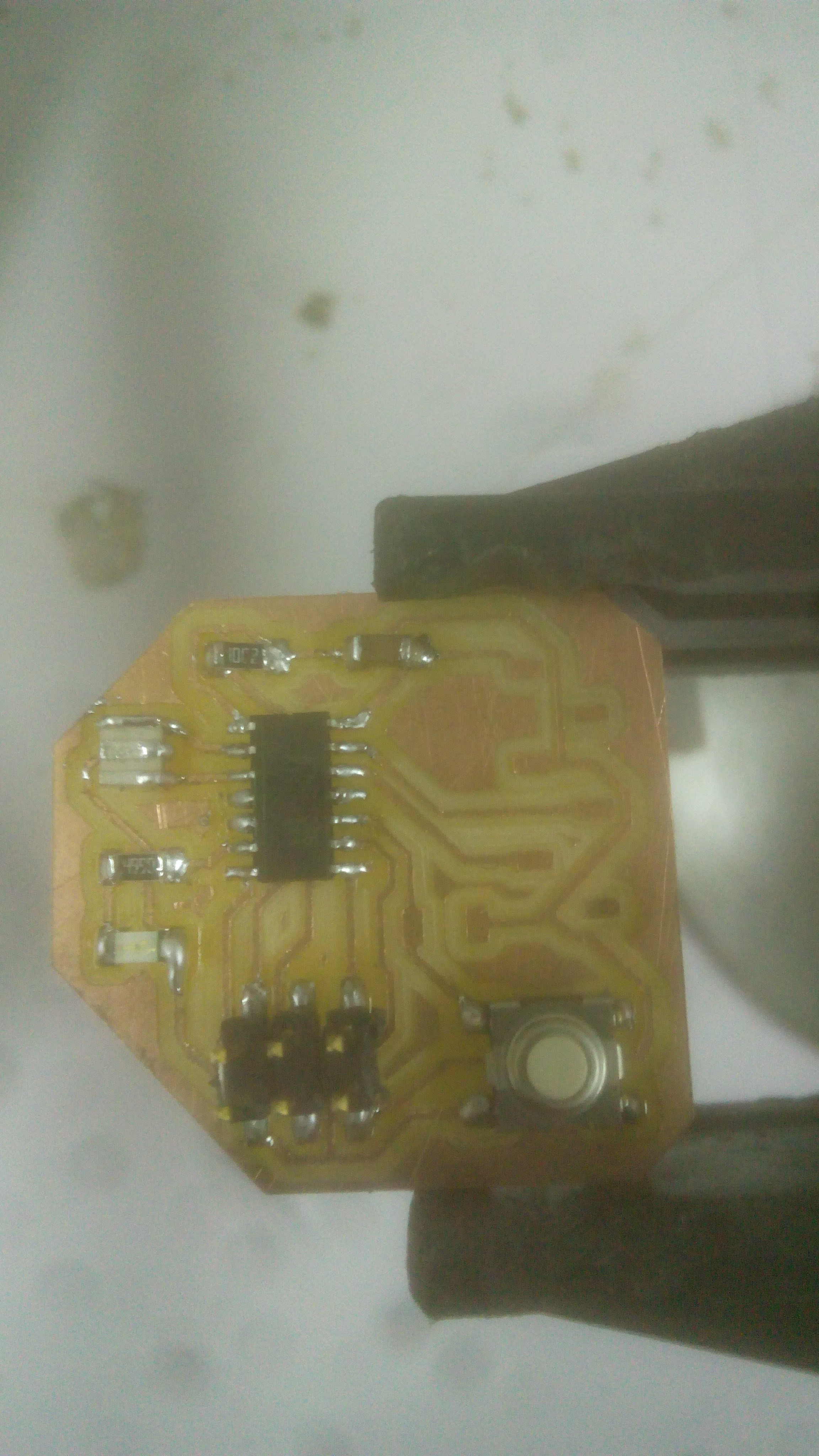
stuffing and soldering
These SparkFun tutorials were really usefull.
And here a gif describing briefly the steps I made in stuffing and soldering.
one of the key tips is to put a little piece of melted soldering on the foot print of one leg of the pcb and heating it again with the corresponding leg while putting the component.
it helps on stabilizing the component and make it easier in soldering the next legs.
the next pictures are about soldering process steps.
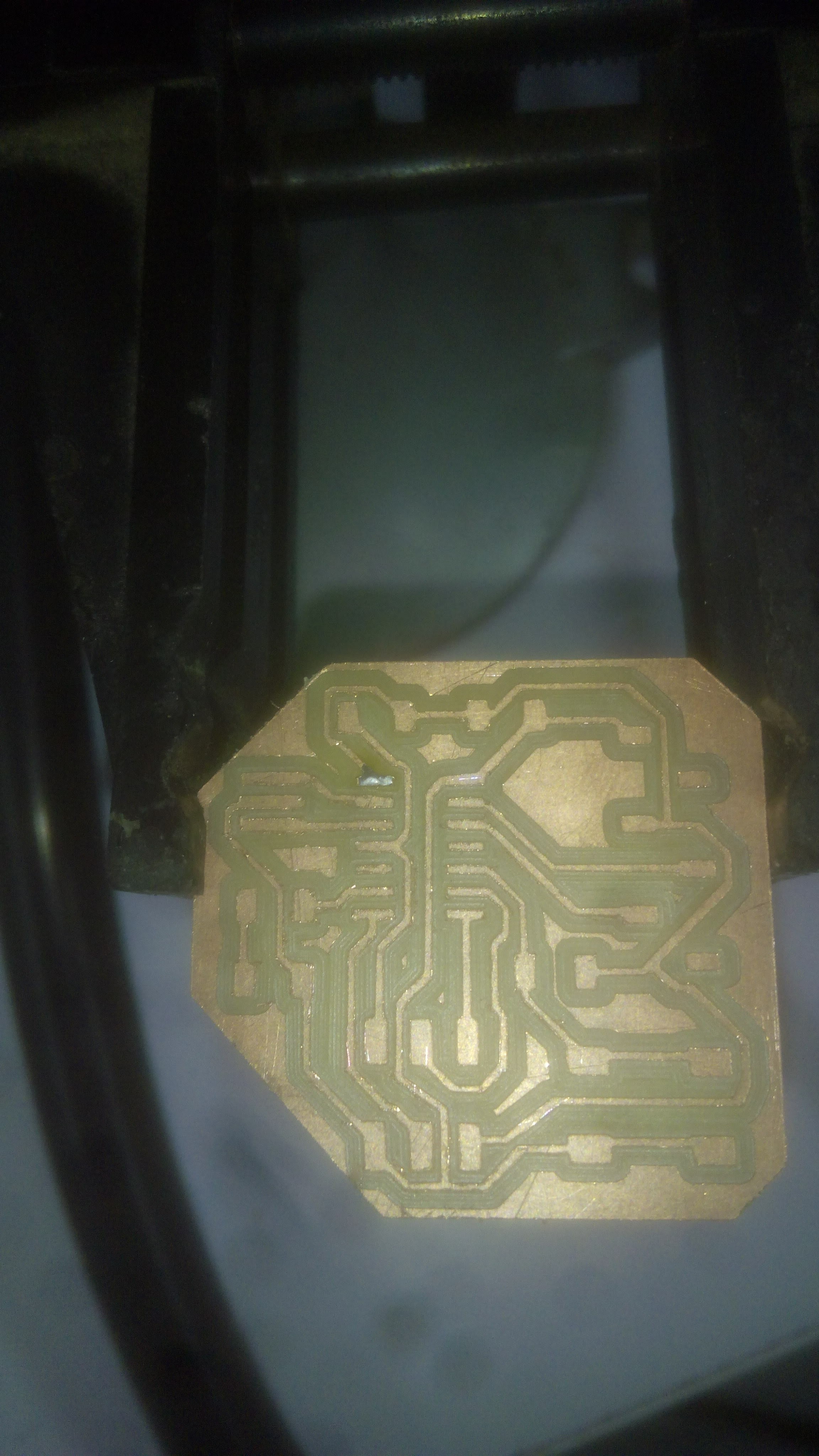
fixing the pcb
putting the first piece of solder
soldering the first leg
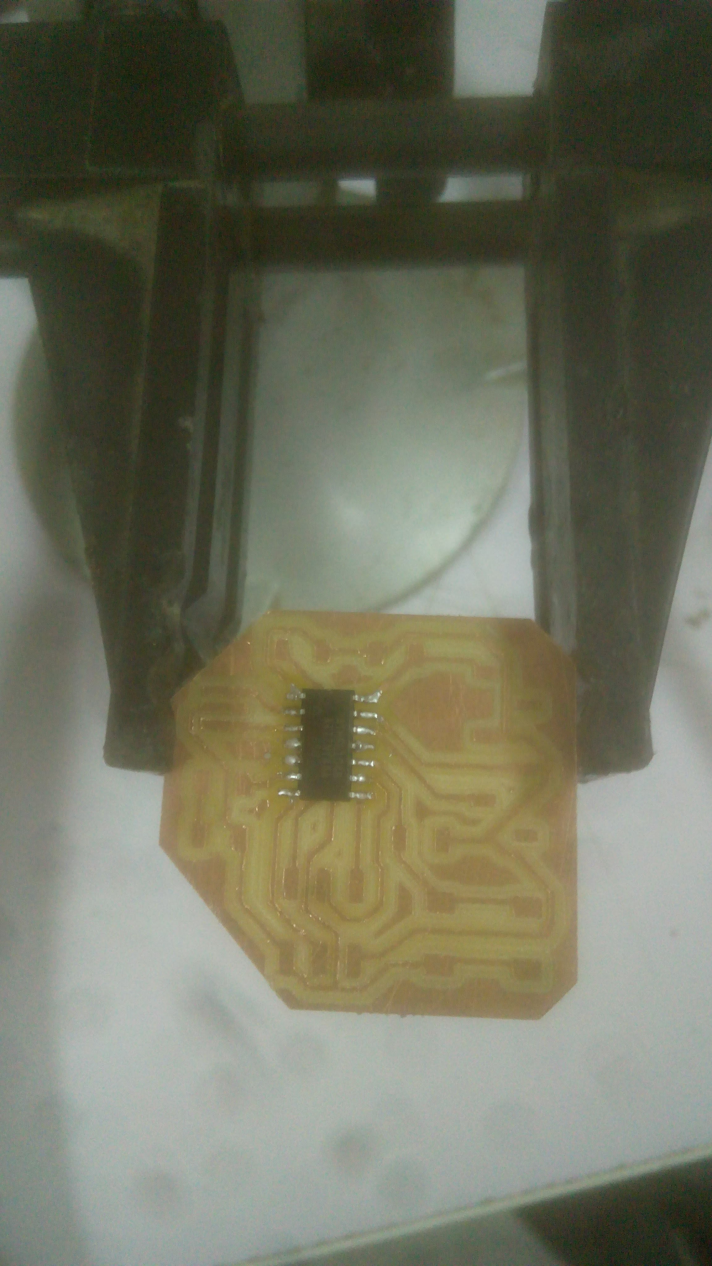
Soldering the rest of the legs
more steps
more steps
more steps
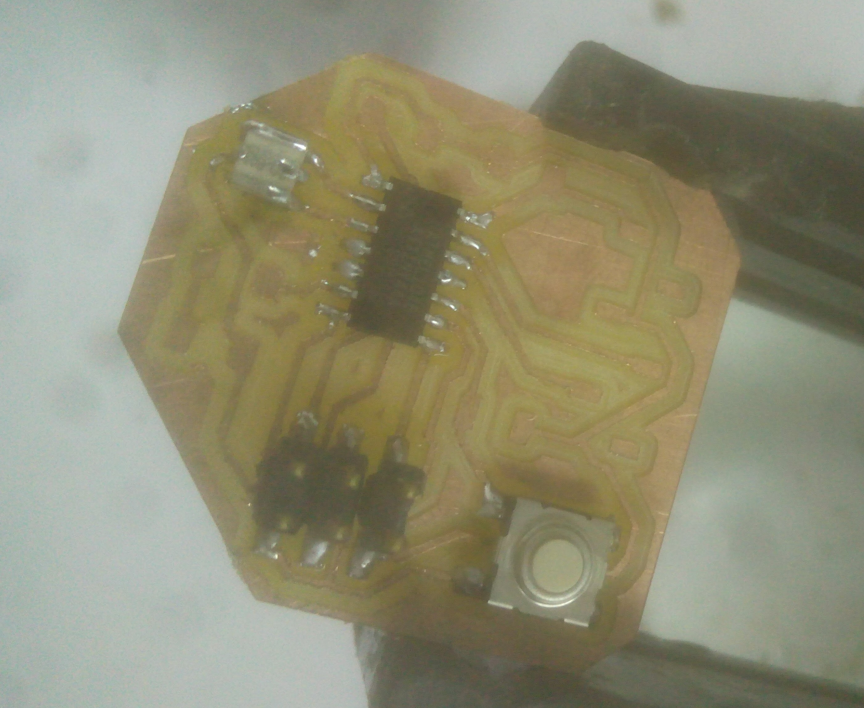
more steps
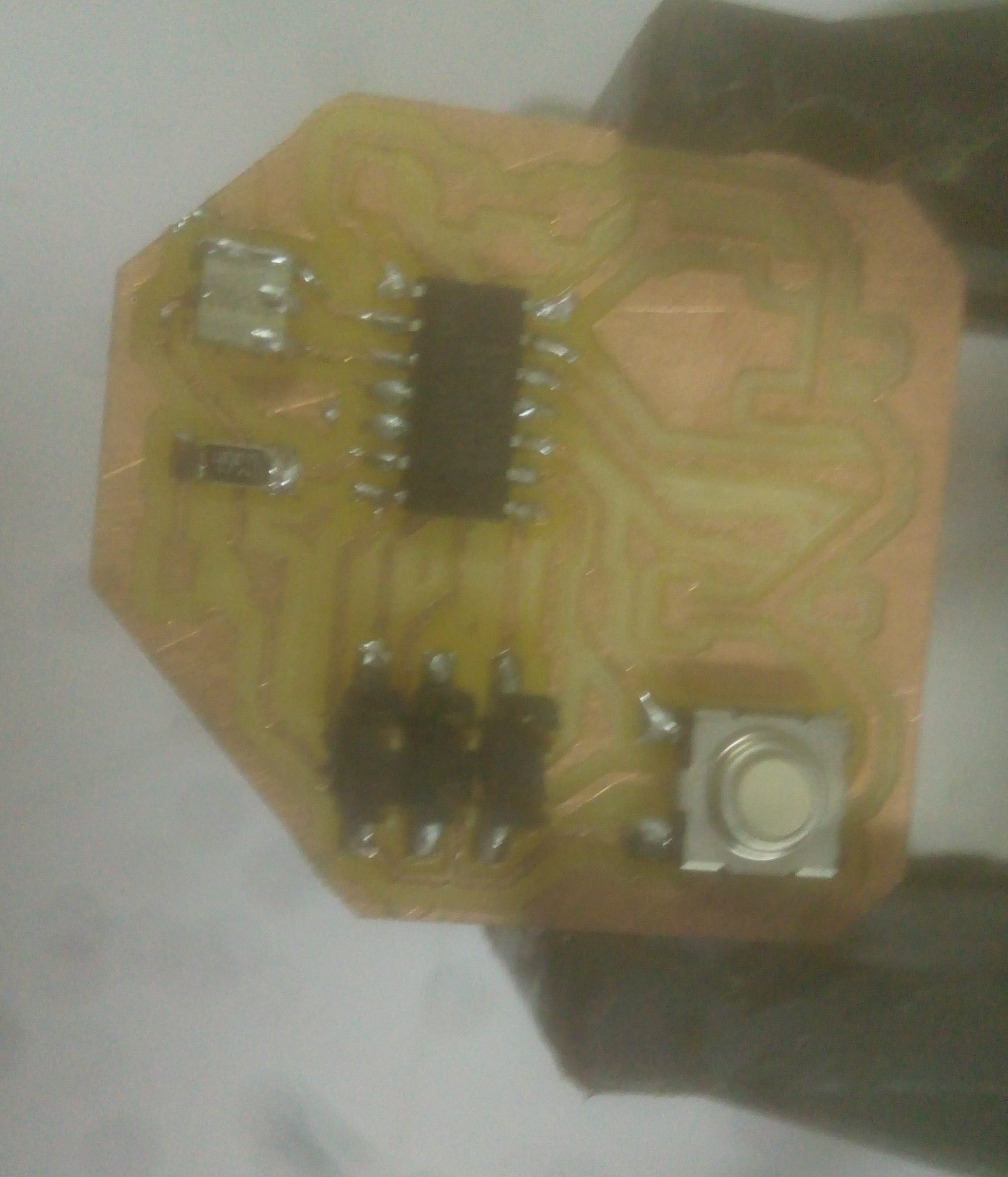
more steps
more steps
more steps
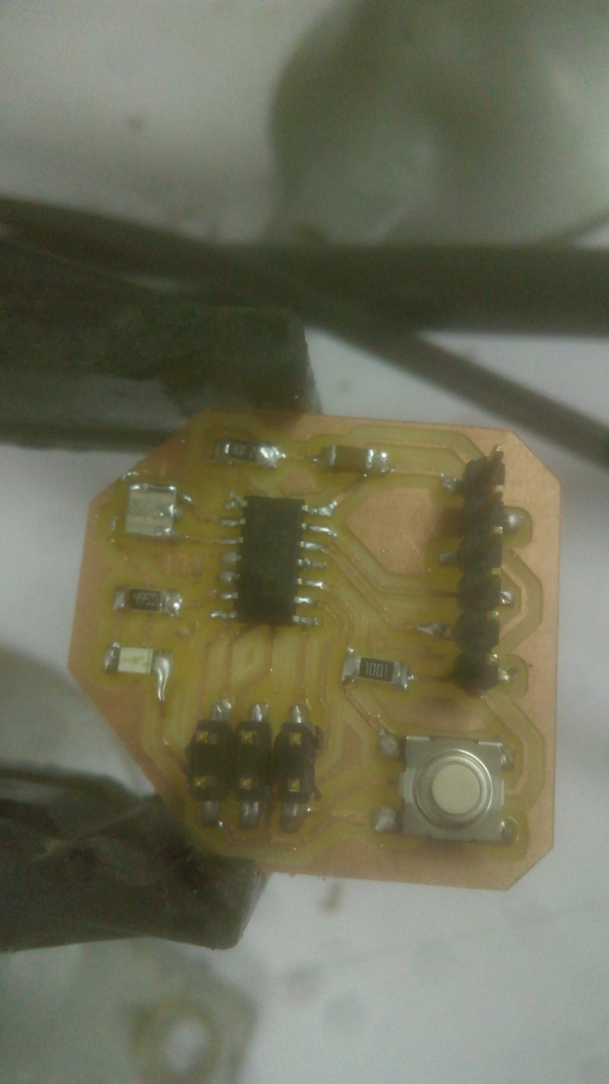
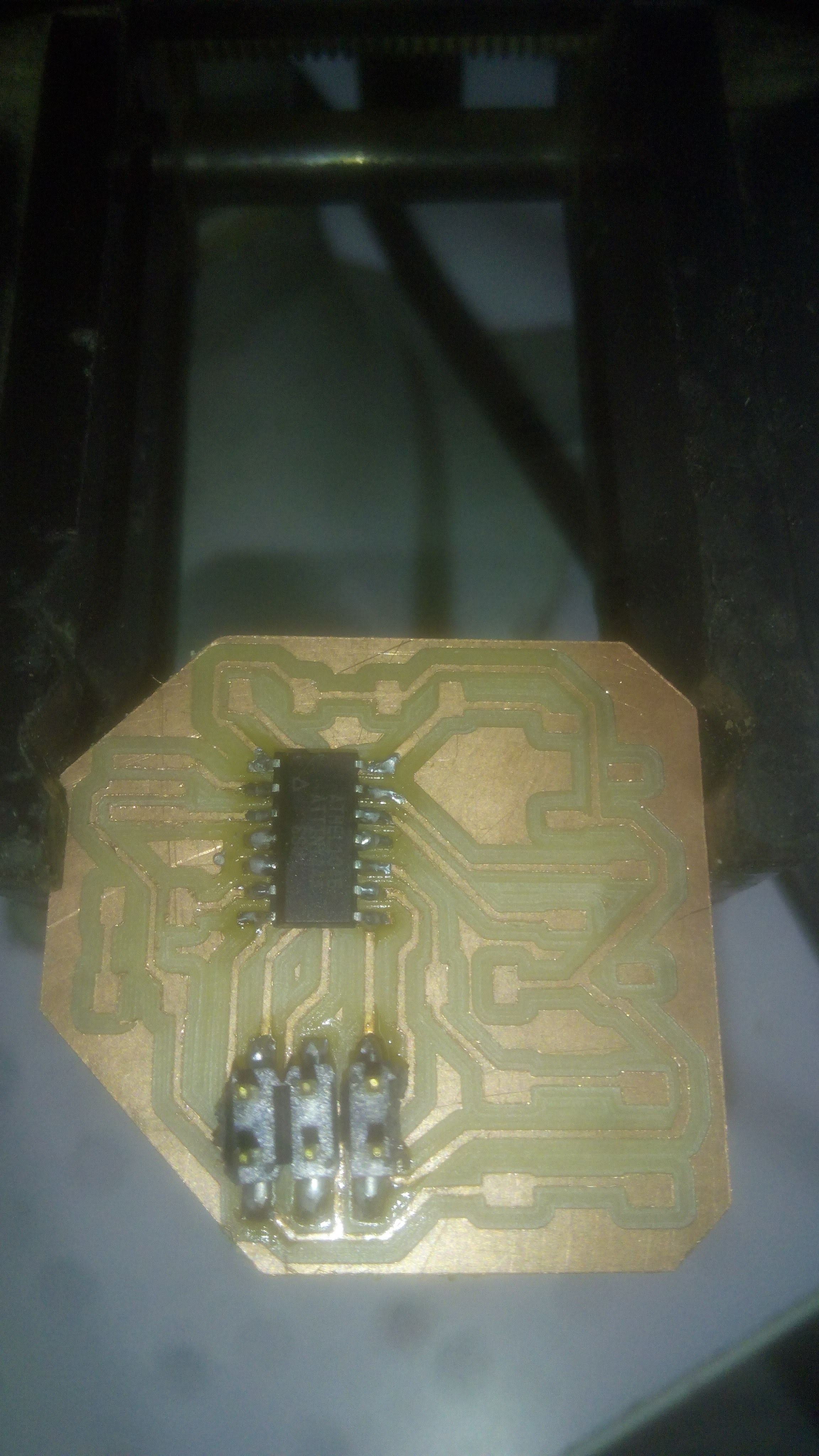
after soldering