Week 6 - Electronic Design
Designing our own board on a PCB design software like Eagle

The weeks objective is to allow us to design our own "Hello Echo" board, whose function was to send a repeated message over serial monitor, and add atleast a LED and button to this board successfully.
Software selection
Options include
Eagle (Free) | KiCAD (Open Source and Free) | OrCAD Lite
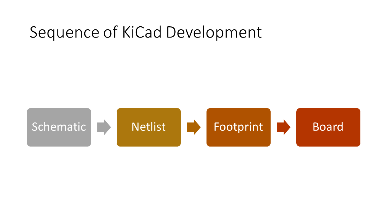
I chose Eagle as the first software, as it is free with a Commercial license free for students for 3 years. Installation is simple, with you downloading the software from its link here. It basically decompresses into a folder of your choice. The processflow of Eagle is simpler, like this

Discarded choices
- Orcad Lite - is not compatible with other softwares, or their libraries. Resulted in immediate disqualification
- KiCad - very powerful, but has a steep learning curve. While eagle has a simple button to take components from the schematic to the board, KiCad uses this flow
- EasyEDA has a great library, and easy to use. It however has conflicts with the Fab library over footprints and as a student, I chose to prioritise development over conflict resolution.
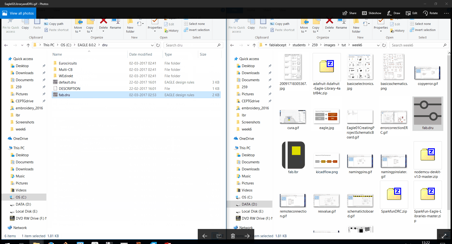
Setup
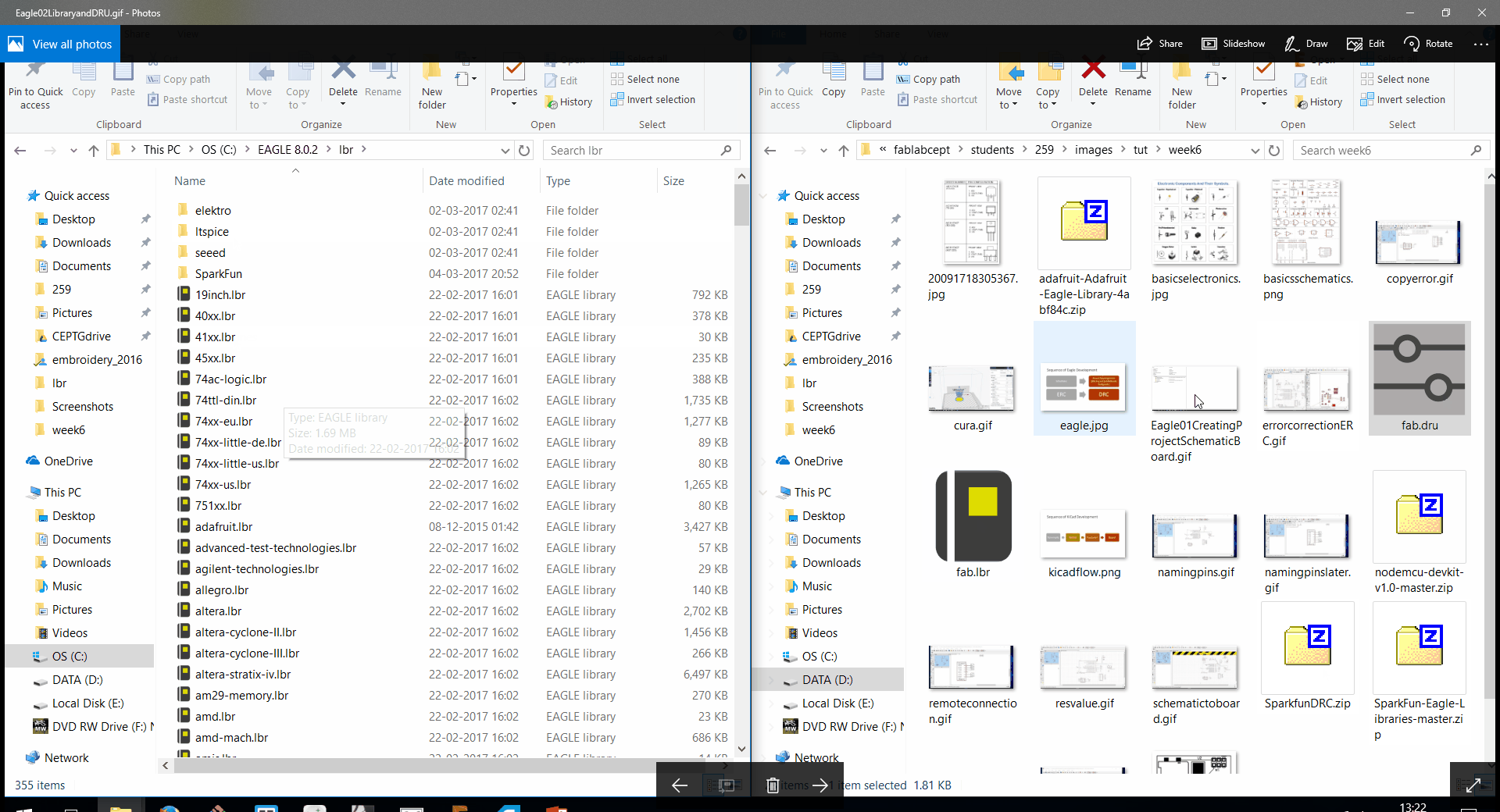
This has 2 critical folders for us to note which we will use - lib and dru. Lib includes all the library files we will end up using to amke our designing easier. THese contain package (sizes) of the components we want to use, its device versions and symbol. DRU includes the Design Rules like track width, more examples below 

 . we can use to test the validity of the designs we make on the PCB so that the designed file is correct.
Links to important libraries and DRU files
- Fablab component library
- Fablab DRU
- Adafruit Component Library
- Sparfun Component Library
- NodeMCU library for me
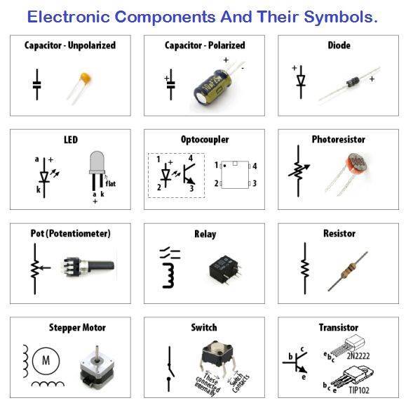
Electronics 101 before we proceed

 Useful link to convert mm to mill here.
How was it done
- Process flow was thus
Click on each image to see a gif image
Schematic is created, errors are checked through the ERC aka Electrical Rule Check. Then a Board is made from this schematic. The board is laid out, connections are routed, and using the FAB DRU, a DRC is done. Click here for a great tutorial on good PCB design by SparkFun. - I used eagle to design a series of variations in board design
- Setting up an eagle project, creating a schematic and a board

- Setting up library and DRC for use
Copying files into the necessary folders 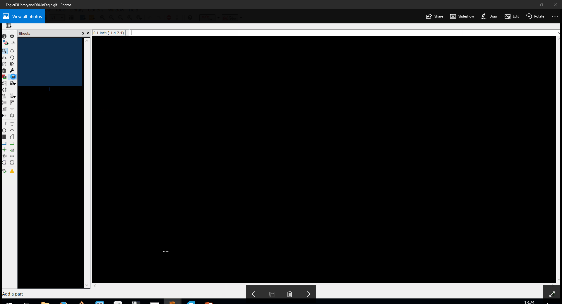
Setting up things in Eagle - Schematic: Making the Schematic and ERC - sample board. I have used an example board in this .gif example. I made my own board for my work.
 Once the Schematic is completed, and an ERC is completed, click ton SCH to BRD icon to go to the Board file.
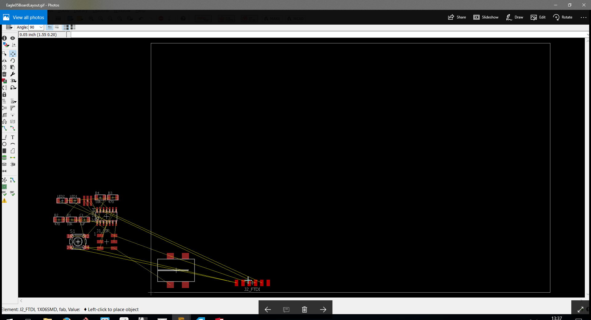
 - Board: Layout, RATSNEST, AUTOROUTE, Manual Routing, DRC and Exporting.
Board layout - move, rotate components. Yellow line is based on connections made in schematic, and will autorotate as you move the component. Autoroute uses these lines, called Air-routes which are used to represent the connections done in the schematic. These are indicative. We can choose to do any layout of our choice.
RATSNEST and AutoRouting - RATSNEST checks these airroutes and finds the most optimised paths. Defining the Trace Width and Gap at this stage ensures that Autorouting takes these requirements from the Menu Option "Net Classes" under the Edit Menu head and uses it to set the width of a trace and the gap between them. Autorouting then uses airwires as the connections to be done and then calculates different paths till the options which achieve all connections is found. Hitting evaluate button allows you to see unconnected paths in yellow (airwires).
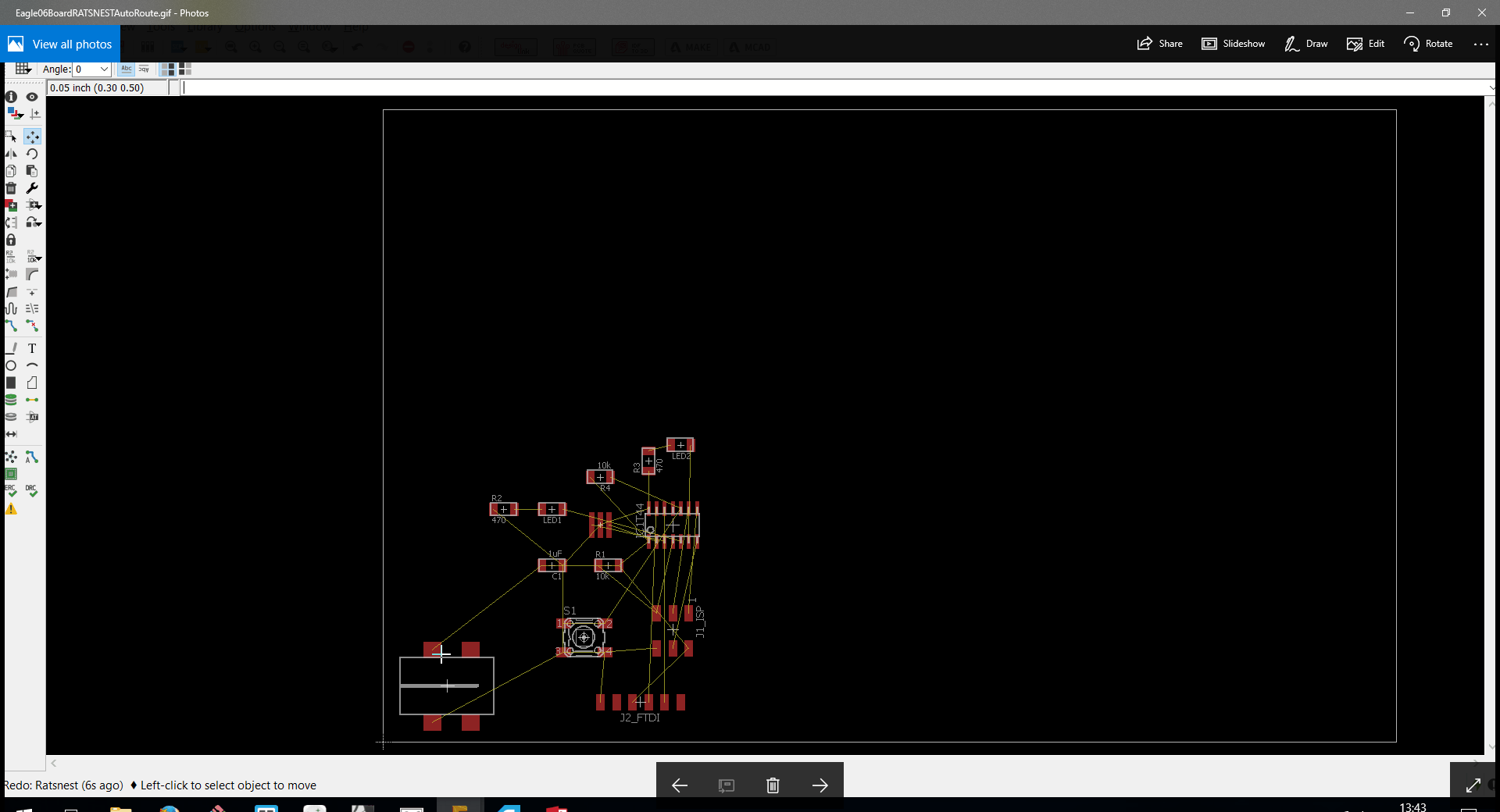
This second gif shows how to modify the autoroute settings to match the DRC needs
Exporting to a .png such that Modella can mill it can be done like this
Sample Schematic and Board and PNG export is here for your reference. PS - this demo is missing a 12v-5v Voltage regulator so that one can add thier own bit into this design.


Assignment
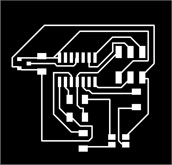
The assignment requires us to redesign the Hello Echo Board with a button and led. The base design was available here as the component view,traces view and outer traces.
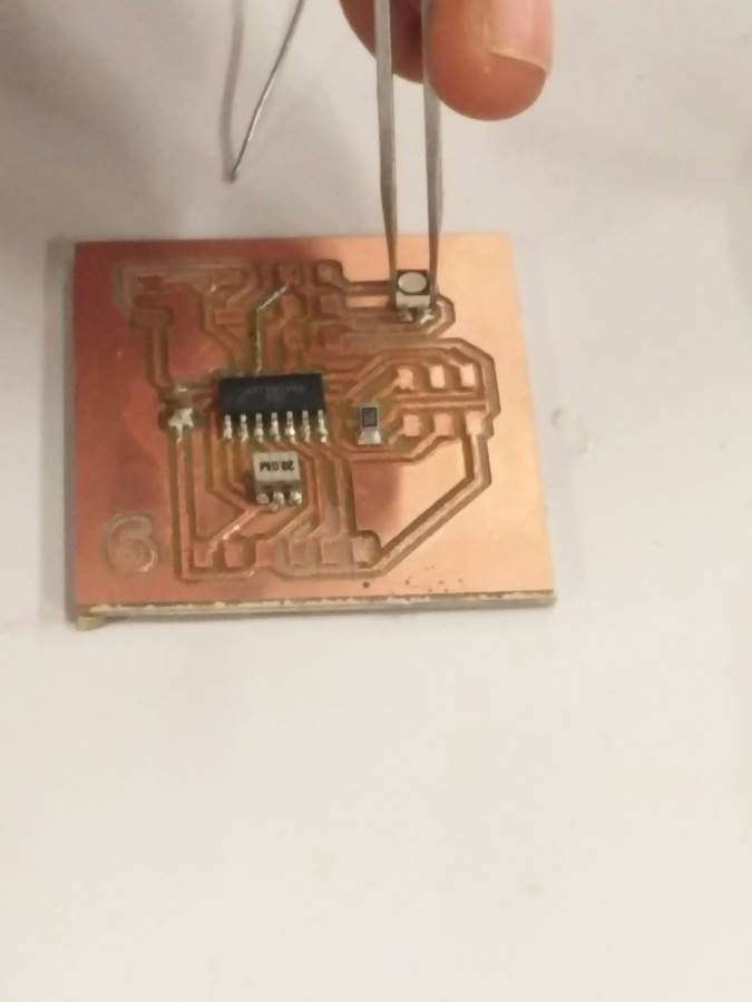
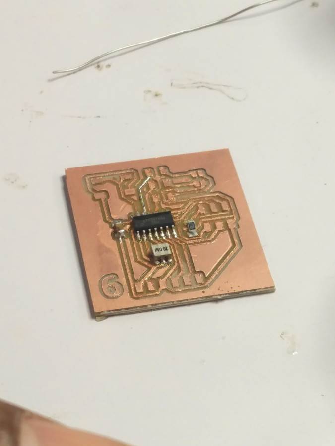
I completed the assignment with this  I also used this opportunity to cut the same design in copper tape using the vinyl cutter.
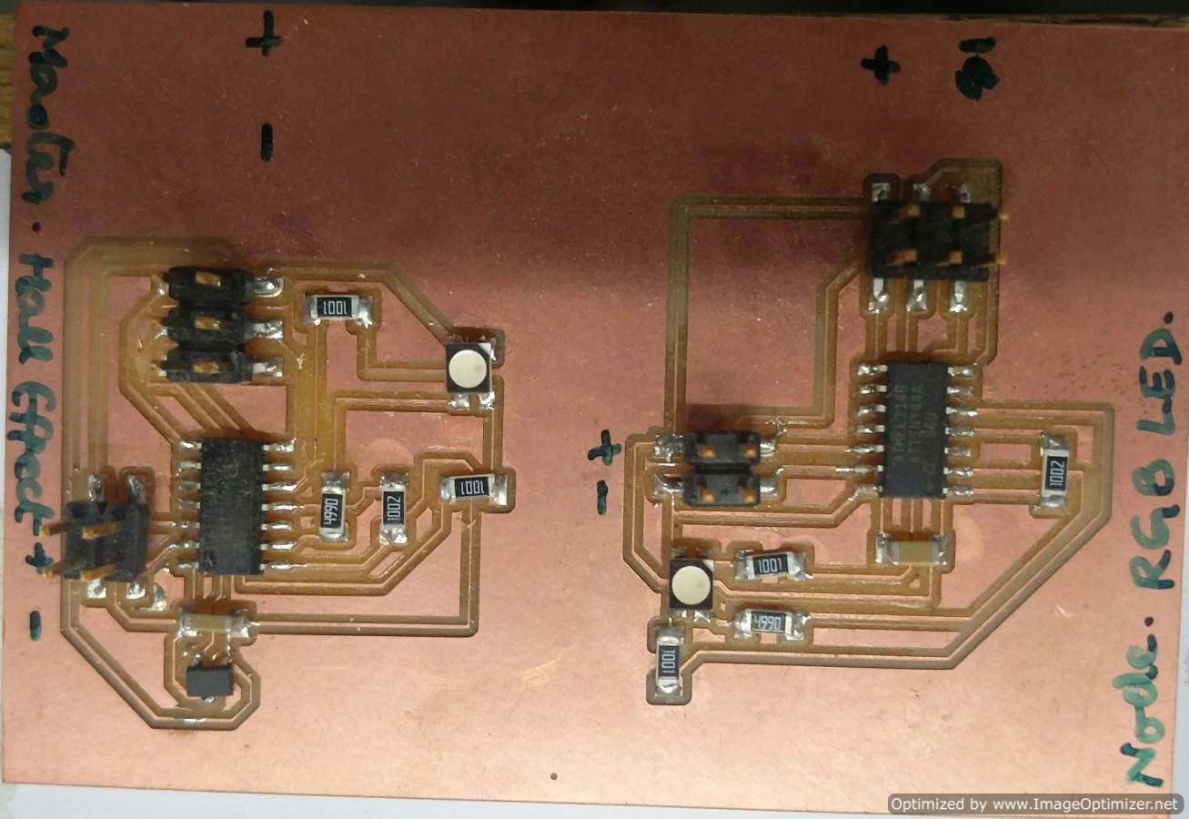
Other How-tos, Mistakes and errors


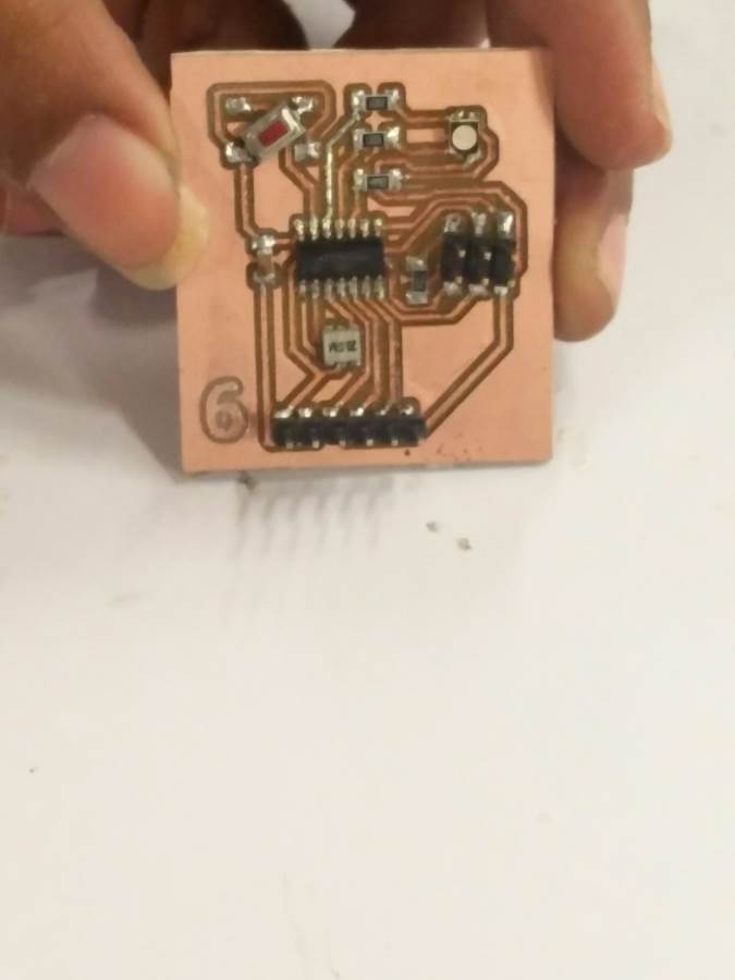
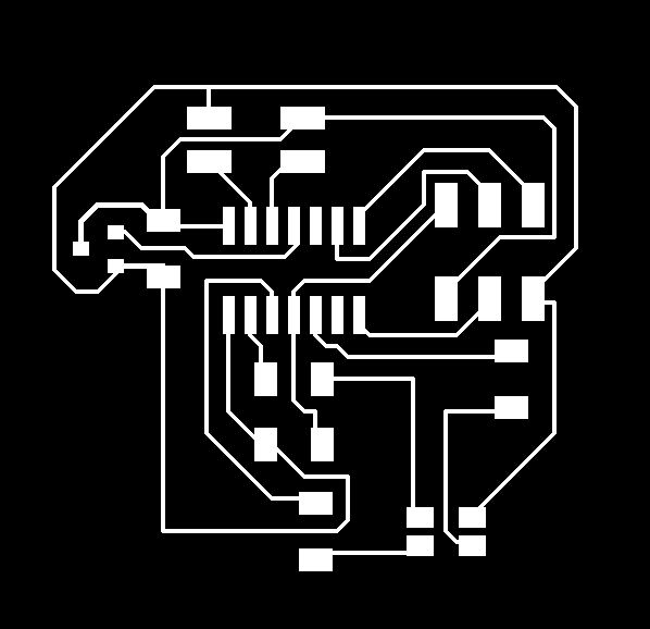
Designed Hello EchoWorld Board and Designed Hello EchoWorld Schematic
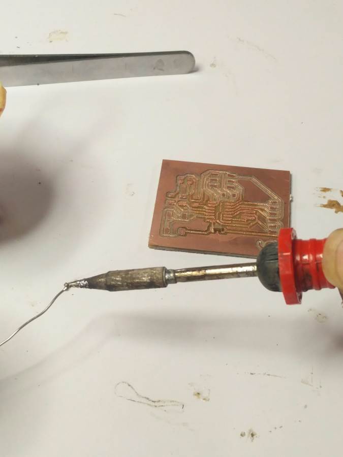
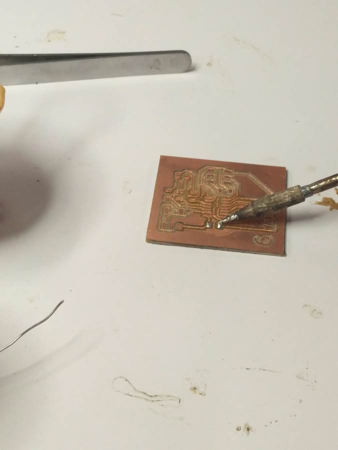
PCB Milling
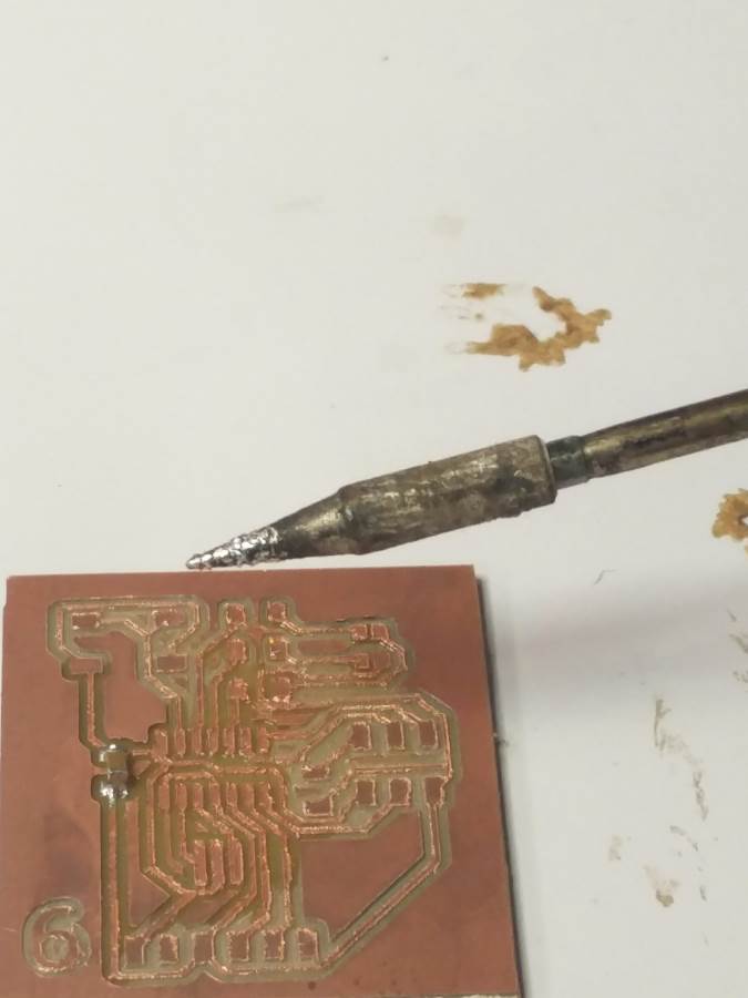
I made 3 PCBs, getting it right on the 3rd attempt.
 Attempt#1 failed (top PCB, left size milling) as I didnt see if my bit was worn out like shown below

 Attempt#2 failed (top PCB, right side milling) as the lines were too close, as I chose to overrule the DRC.
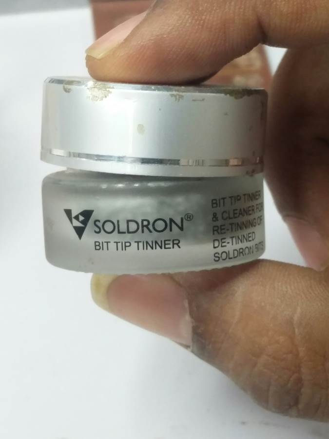
Soldering the Hello Echo Board
How to Clean a Solder Tip from Gautam Prakash on Vimeo.
Week 6: soldering the ATTINY 44 from Gautam Prakash on Vimeo.
Week 6: Using a Multimeter to test the RGB Led from Gautam Prakash on Vimeo.
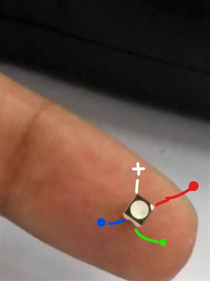
Week 6: Testing the RGB LED after soldering on board from Gautam Prakash on Vimeo.