Electronics Design
In this week we have to design a PCB circuit and we were assigned the following tasks
1. Redraw the echo hello world board
2. Adding at least a button and an LED with current limiting resistor
3. Checking the design rules and finally make it
4. Extra Credit: Simulate its operation
5. Extra Credit: Measure its operation
Learning outcomes of this week
1. Select and use software for circuit board design
2. Demonstrate workflows used in circuit board design
There are many software for circuit board designing available on internet as an open sources but I chose to work with EAGLE 7.5

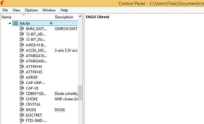
To accomplish the assigned tasks I started by downloading and installing the Eagle 7.5 software and as I was suggested to use components from Fab Lab invenotry so I added the FAB LAB eagle library fab.lbr to my installed version as shown in figure below.
Components required
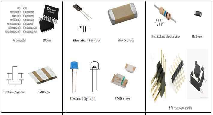
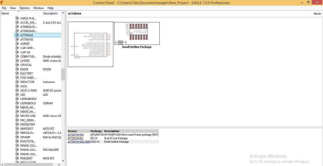
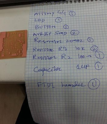
1. Microprocessor: It is computer processor which incorporates the functions of central processor unit of any computer machine on a single integrated circuit. here to design this hello board our required micro chip is Attiny 44SSU(IC1 t44) in my design this micro chip is the central part of the whole circuit.
2. Capacitor: It is a passive electrical component that is used to store the electrical charge. I m recommended to use Ceramic capacitor of 1 micro Farad capacity.
3. Resistor: It is also a passive electrical component. Basically it is used to convert Electrical energy into Heat and light energy but in small electrical circuit it is used to limit the current flowing in the circuit here in my design I have used three resistors, two resistors of 10 kilo ohms and one of 499 ohms.
4. Resonator: It is an electronic component consisting of a piece of a piezoeletric ceramic material with two or more metal electrodes attached. it is used to generate an oscillating signal of a specific frequency. here in my design I have used 20 MHz resonator (XTAL1 20MHz)
5. LED (Light Emitting Diode): It is semiconductor diode which glows when a voltage is applied. Here in my design the LED plays the part of an indicator for the device so that actions to be performed on device must monitored and evaluataed.
Additional Components for the compelition of circuit
1. Two 2x3 SMD six Head
2. Switch Button
To design any electronic circuit in the eagle mainly we take two things in account i.e Schematic Design and Board layout Design So I started working on schematic design in schematic editor which allowed me with easy way of designing the circuit.
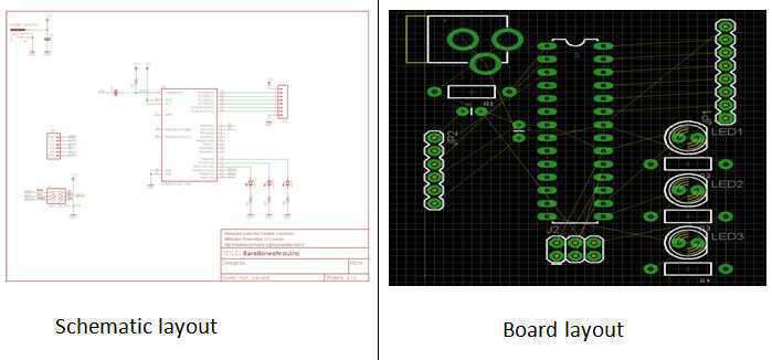
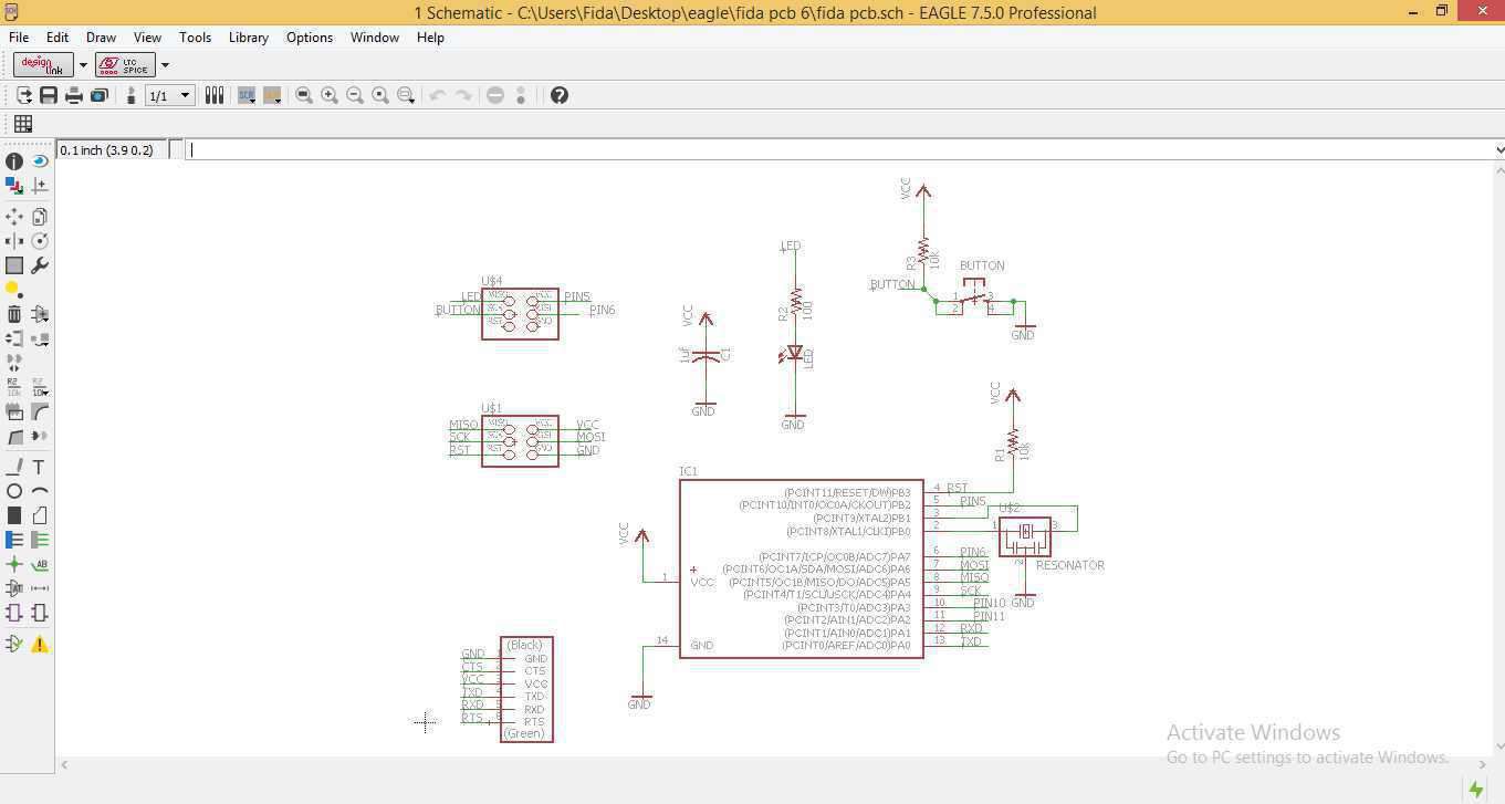
First I import the required component of my circuit from the library and add one by one to schematic editor and after labeling the terminals of every component imported to the editor I got my schematic ready. following image is of my schematic design.
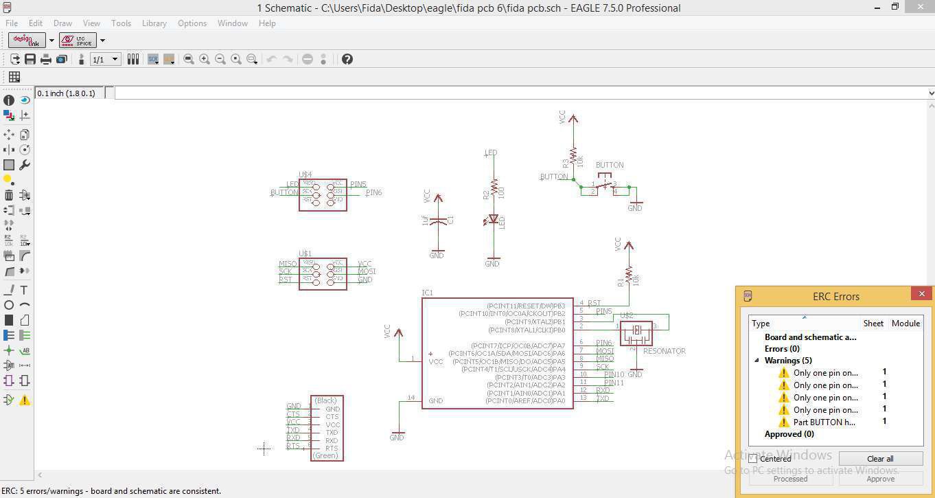
After getting the schematic ready we are supposed to check ERC i.e Electrical rule check characteristics, here I got zero errors but few warnings and in most of the cases warnings are appeared due to pins which are left un used in the circuit. So far in my case the circuit is ready for the routing for achieving the board lay out. here is the snapshot showing the ERC situation.
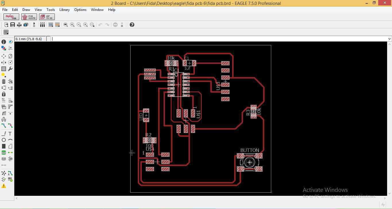
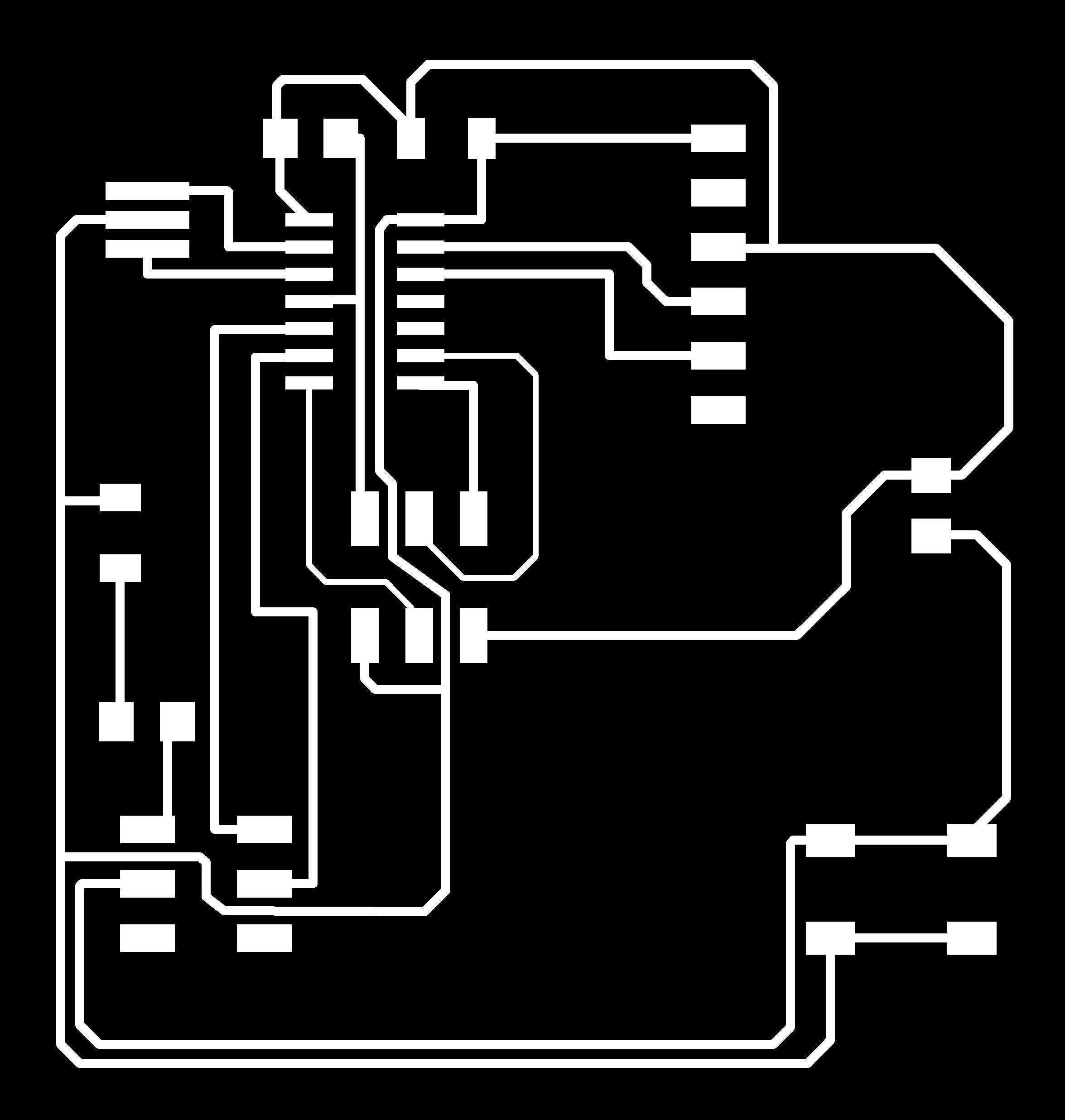
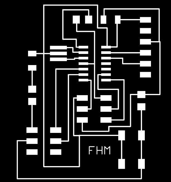
After checking the ERC with no errors and few warnings I switched the schematic to the board layout for routing and placement and further more I went under the process of DRC checking here is the snapshot of my design for board layout.
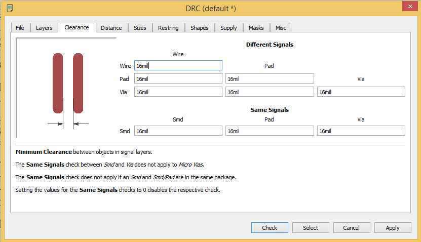
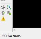
Here is the snapshot for processing the DRC showing no errors with my design. DRC is actually acommand that checks the board against the current set of design rules, without parameters the DRC command opens a design rules dialog in which the board design can be defined and from which the actual check can be started. this means now I can export my design with jpg file.
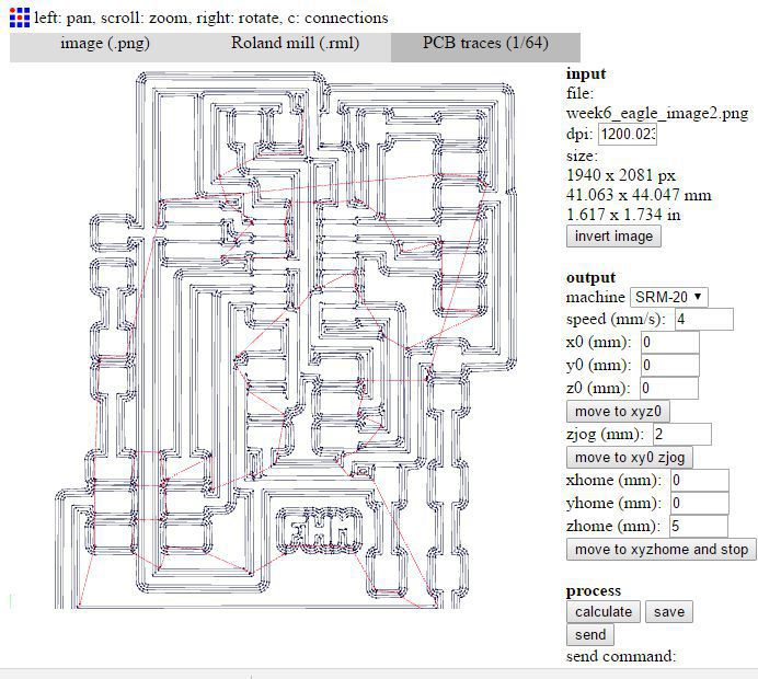
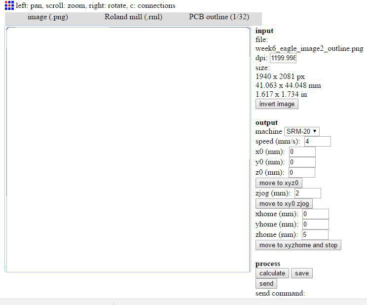
Now exporting the files of board for the process of milling for that in the eagle menu go to File->Export->Image where I select .jpg format for my board design and monochrome with more than 400 dpi i.e 1200 dpi for my board and finally i export the traces file and outline file using Photoshop, below the snapshots are given.

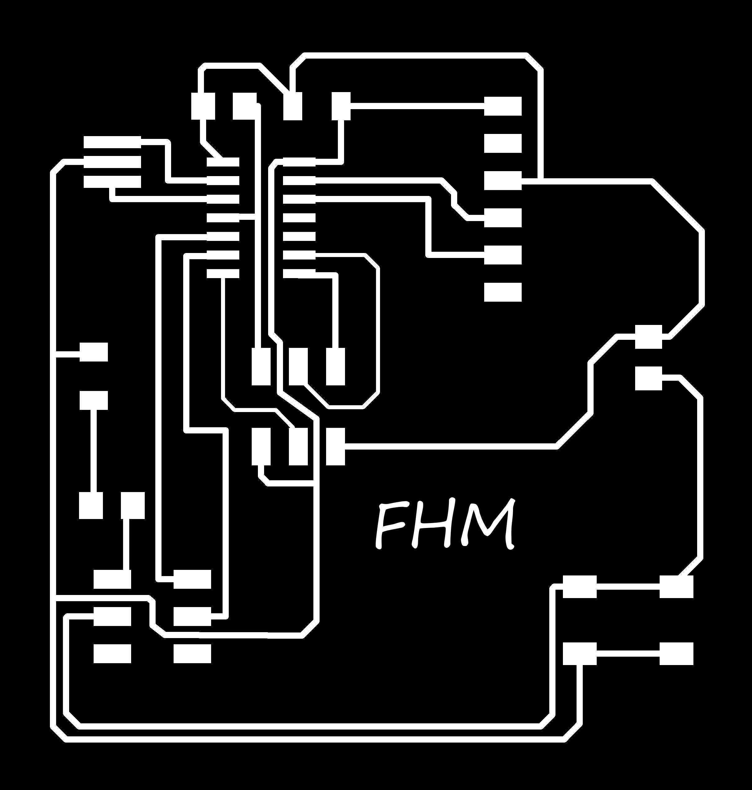
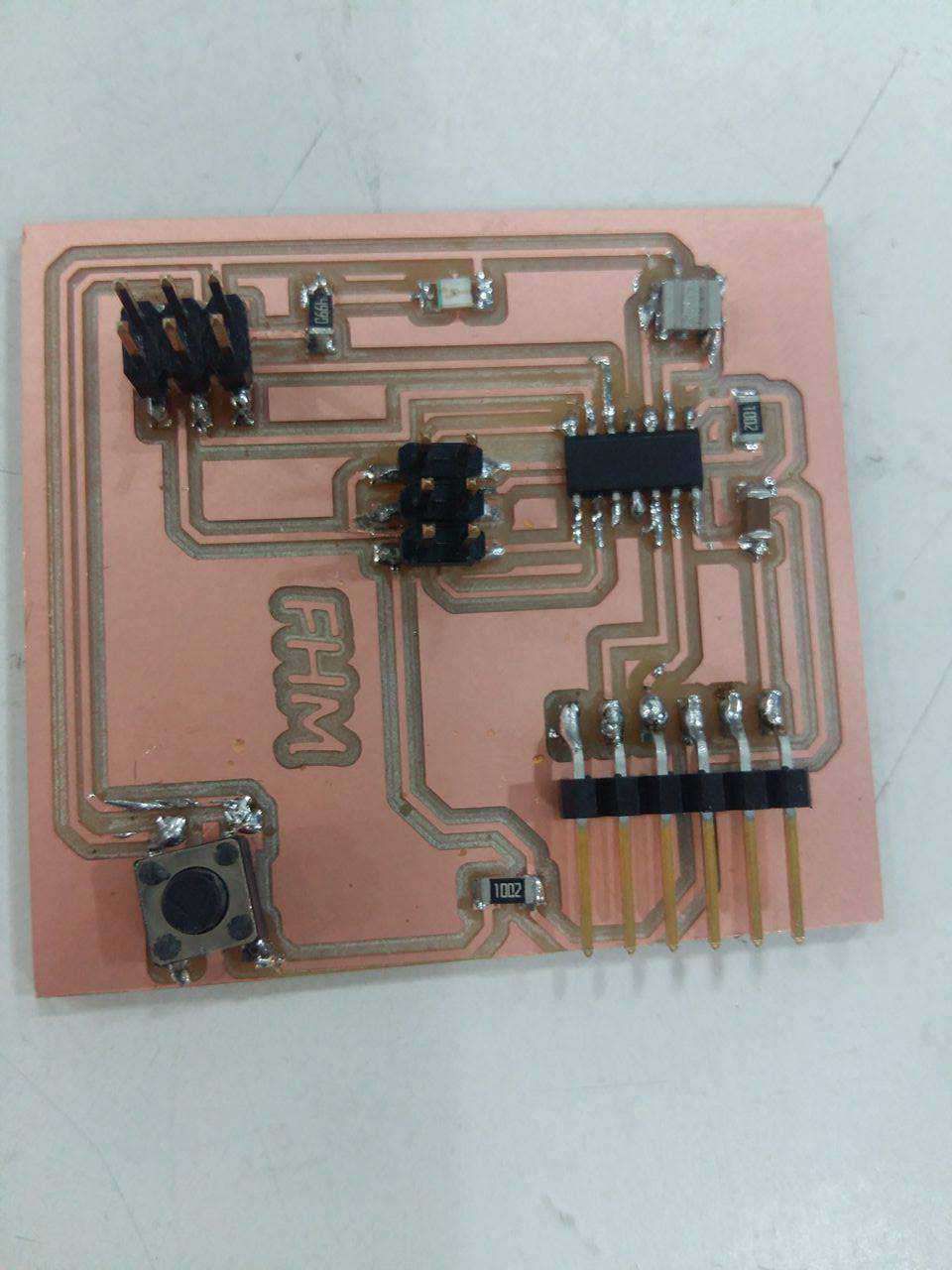
Now as per my own specification I put my name abbreviation FHM as a logo on the vacant space of the board as shown in the image below
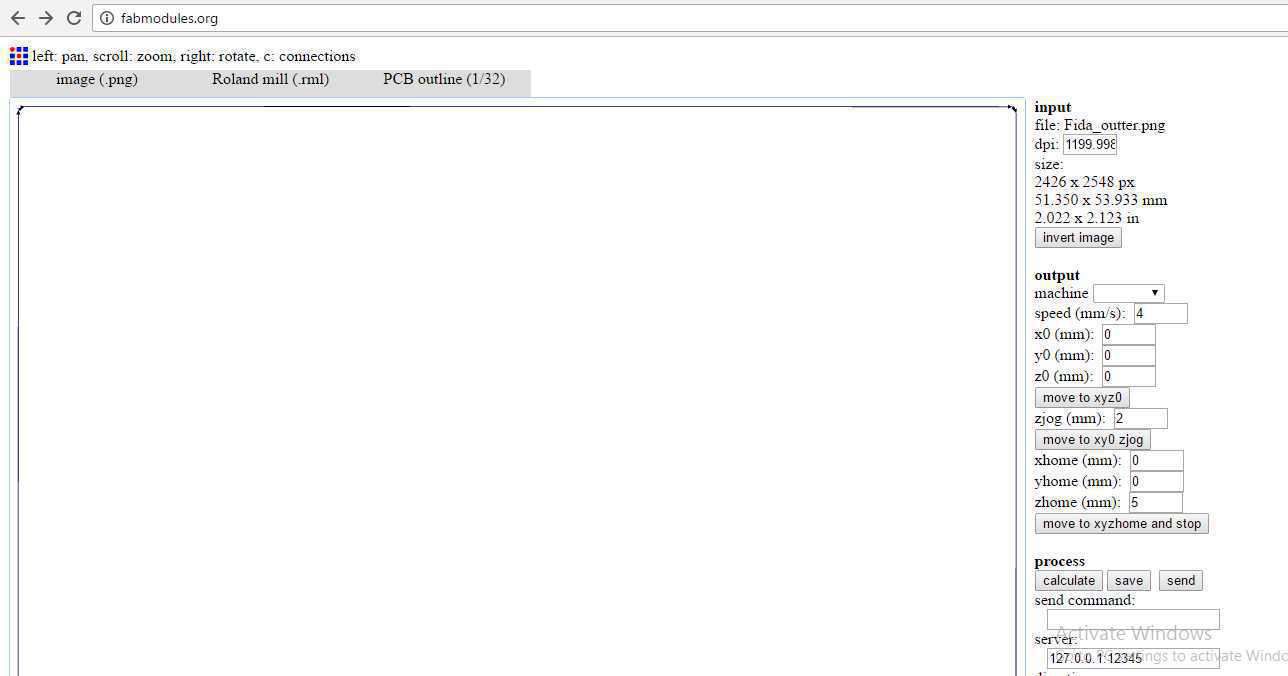
Now its time to export the board in the Fab modules to genrate the .rml file from the .jpg file by setting the follwing specifications.
1. For traces
we have to set cutting tool dimension as 1/64, (X,Y,Z)=(0,0,5) to avoid the bugs and Cut depth=0.1 where as offset value = 4 as shown in the snapshot below.
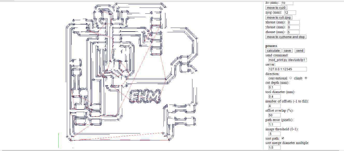
2. For the outlines
I set cutting tool dimension as 1/32, as usual (X,Y,Z)=(0,0,5) and Cut depth = 0.5x3 where as offset=1
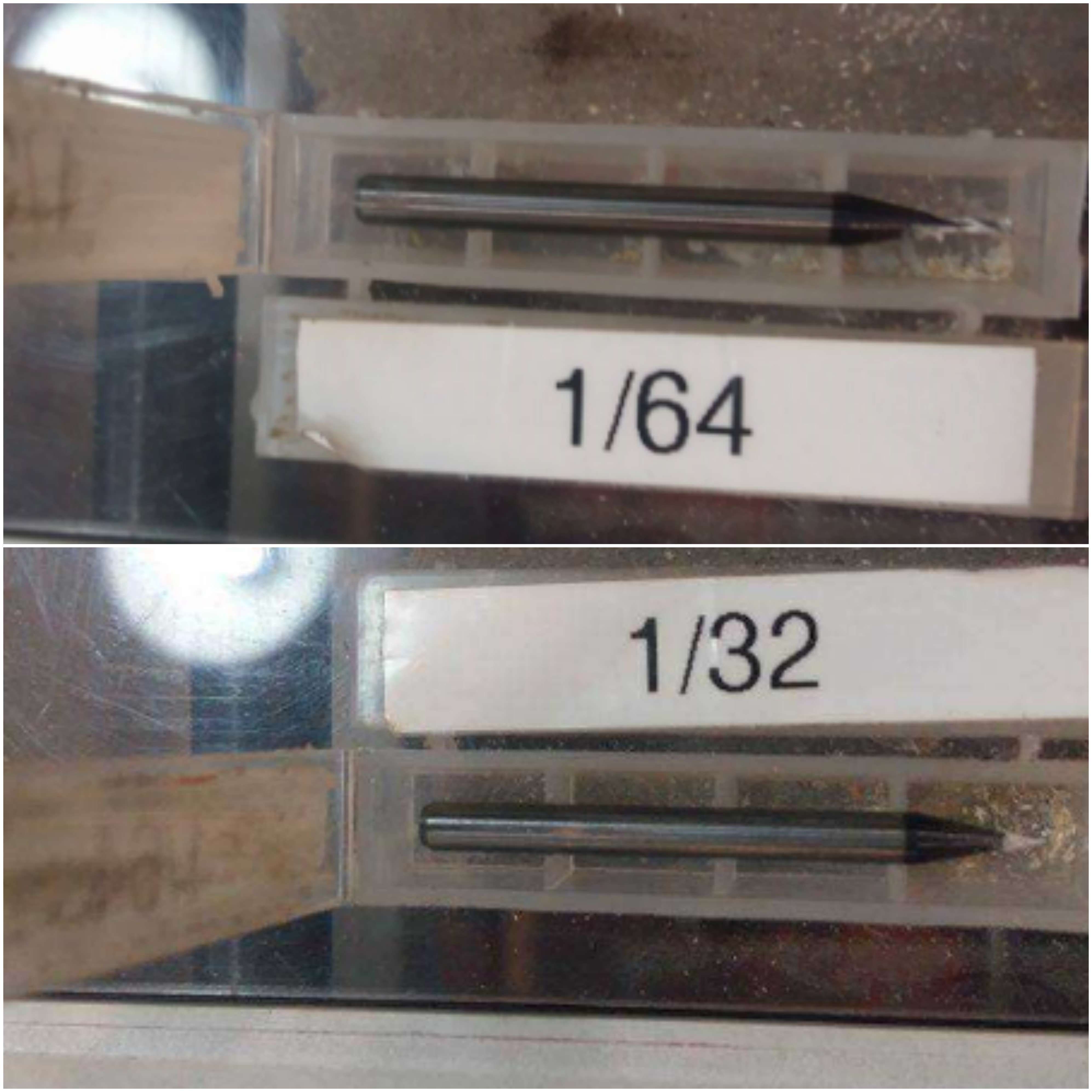
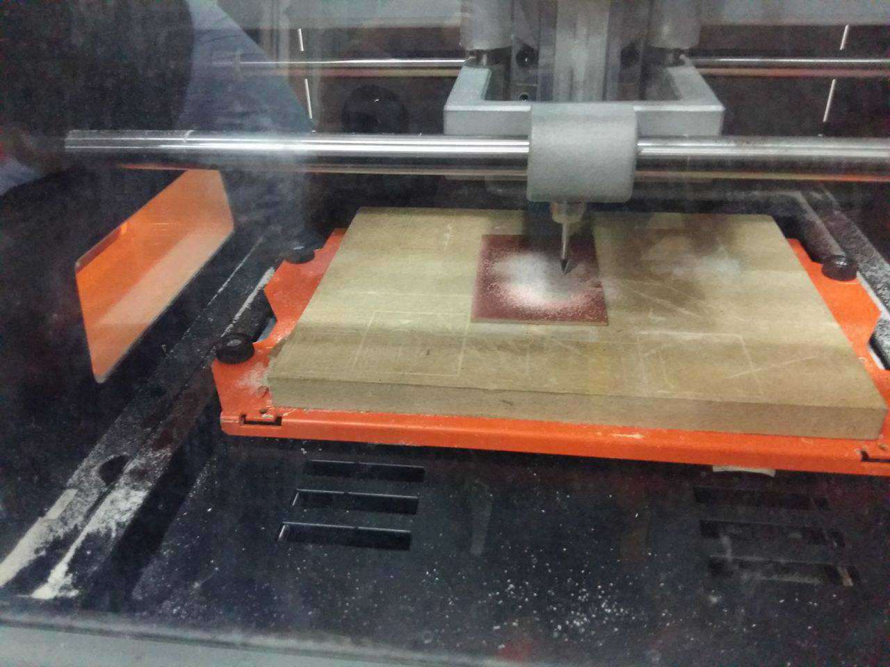
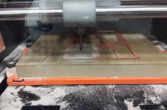
After calculating .rml file for traces and outerline now its time to mill the board for that I have used the mill machine SRM-20 available in the lab by defining XY origin point and Z origin point. Changing the tool mill 1/64 for the traces and 1/32 for the outline. I went for cutting the traces first and then outline and fnally i got my PCB design on the PCB board ready for the populatin the conponents some snapshots are here to observe the process.
The image below is showing the milling of the board in process and after milling the traces as well as outline I started to populate the components on the board.
Soldering the components on board
I repeat the same process of soldering as I did previously in week 4 (Electronics Production) while polpulating the components on Hello ISP board recommended by Neil available at Fab Modules.
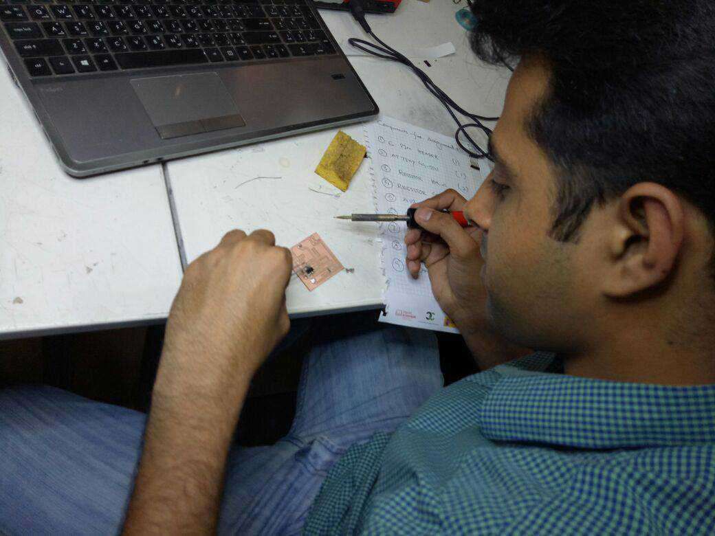
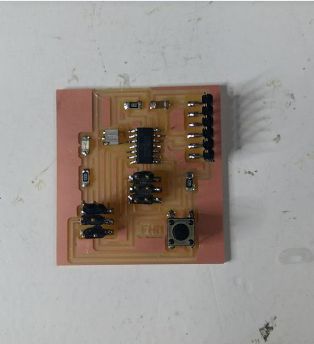
By the complition of populating the components now my PCB circuit board is ready for debugging, As from my board its very clear that I have redrawn the Hello board and added atleast one push button and a LED.
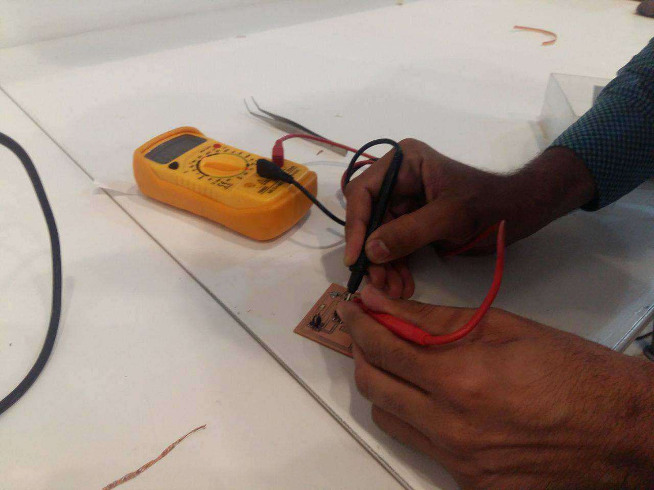
Debugging the Board
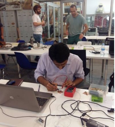
As I started Debugging with Multimeter I actually wanted to confirme that all of the elecrical connections are ok but during debugging I found that two pins in the header were short to each other so I resolve the issue by concerning Xavier and Santi and they guided me to troubleshoot the circuit by resoldering that pin of header and finally the board is now ready for the programming which will be done in week 8 ahead.
Rebuilding the Board
As I reached week 8 in which I have to program the board that I build in week 6 and I was assigned to observe the results but unfortunately I could not come up with said target as the board I build first was not working properly so i thought to repeat again all the process to rebuild the board and I was intent to observe the mistakes I made with first board.
Redesingned the board in eagle
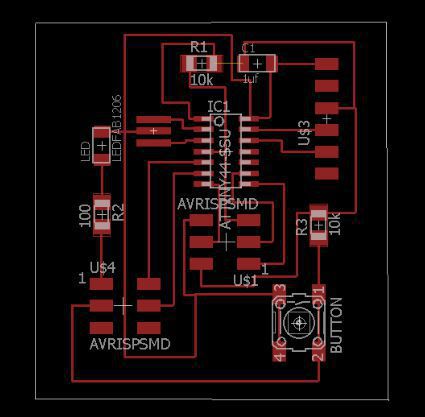
Image files for traces and outlines

Generating Rml for traces and outlines
Milling
Populating the board
Debugging the board using DMM
Finally got new board with OK connections
All the files are avaialble to download from here