06 - electronics design
This week we have to learn to design PCBs and make our own version of the echo hello-world board.
The objectives are:
1 - redraw echo hello-world board
2 - add button and LED
3 - mill and solder the board
Additionally we have also programmed the board.
This is the plan:
Because in my final project I want to make a LEGO compatible IoT kit, I decided I want to try to make the PCB LEGO compatible. To do this, I’m going to use the parametric LEGO construction kit from the computer controlled cutting week and try to replace one part with the PCB. To do this I have to import the dimensions of this object into PCB design software and mill it in the right shape.
Software:
Our local instructor advised to use Eagle, I’m happy with this solution as it is part of Autodesk and integrates nicely with my Autodesk account and files.

Redrawing echo hello-world board
To start redrawing the board, I used this tutorial http://archive.fabacademy.org/archives/2016/doc/electronics_design_eagle.html
First thing to do is install Eagle, after that, set it up.
Once Eagle is installed, download the Fab library that provides you with all the components you need for this board. It can be downloaded here. http://archive.fabacademy.org/archives/2017/doc/electronics/fab.lbr
I put an # in front of the file name so it shows up at the top of your libraries list.(you’ll see why this is handy later)
Put the library in the ‘lbr’ folder with all the other Eagle files, depending on if you’re using a Mac of Windows the Eagle folder may be located in documents(mac) or C:(windows).
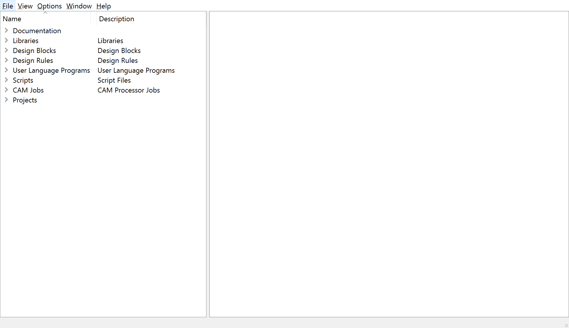
When you open Eagle, the first thing you see is this screen:
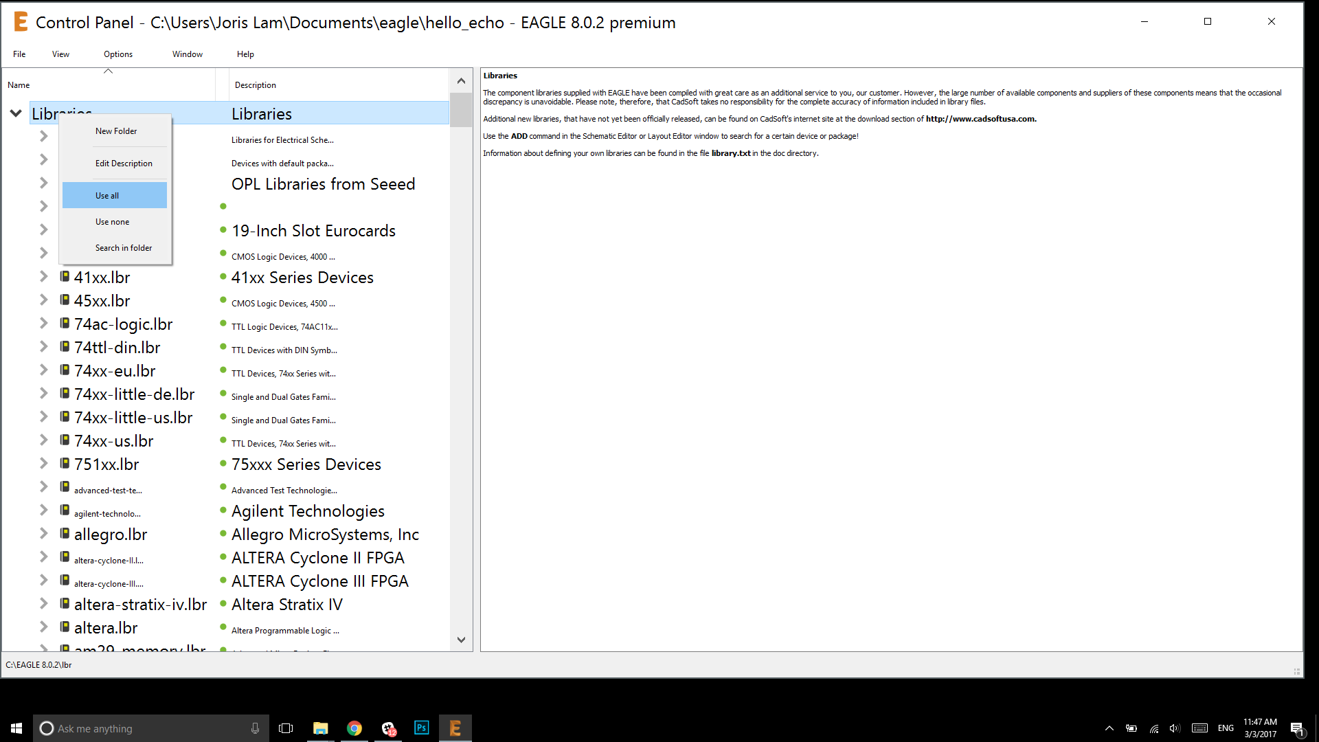
Start by activating your libraries by right clicking on them, and then hit ‘use all’.
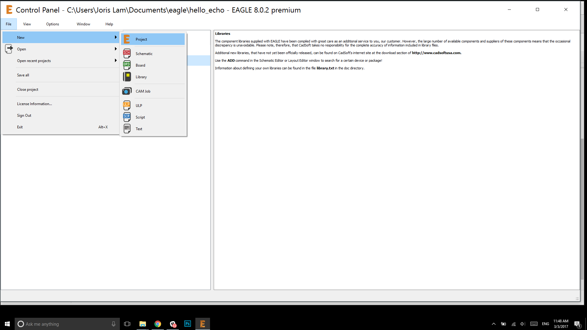
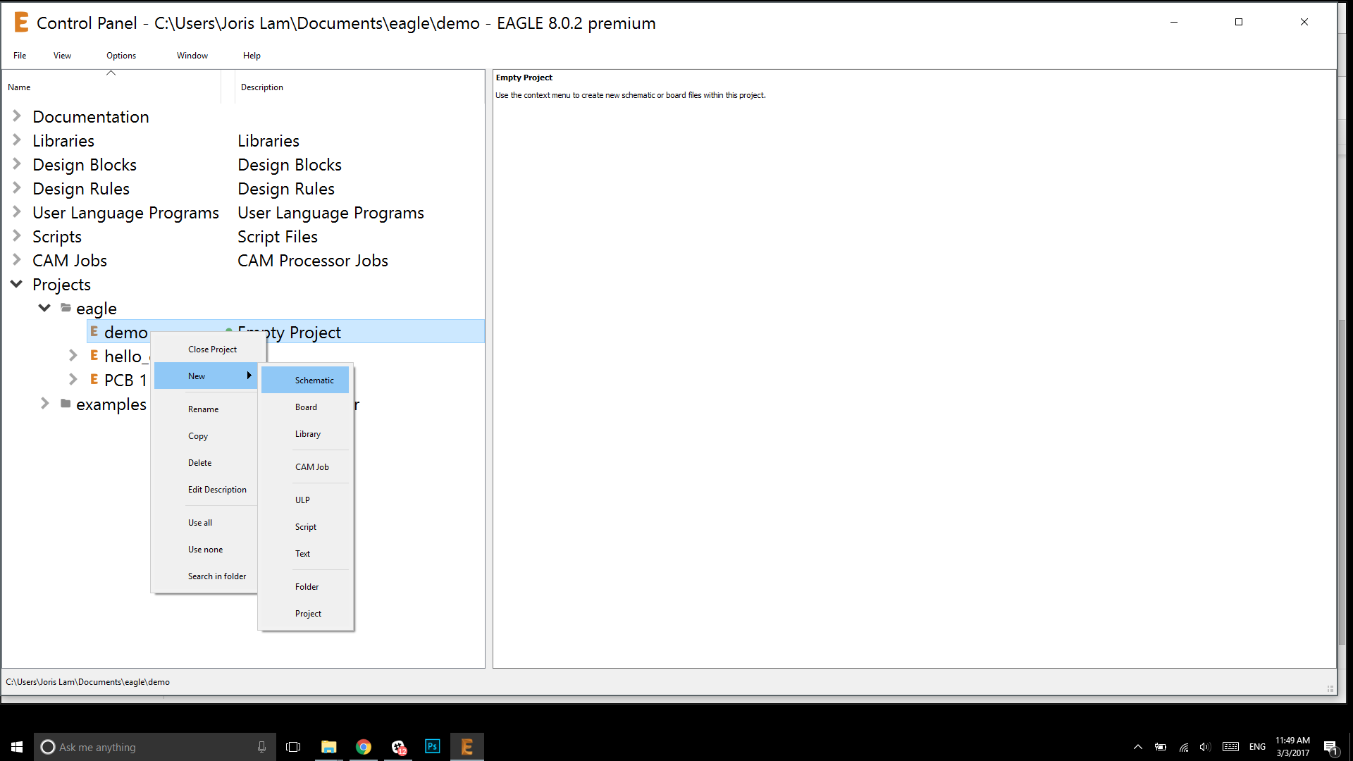
Then go to ‘file’ to start a new project:
In your new project, right click to start a new schematic, don’t worry about anything else for now, it will auto-generate when you need it.
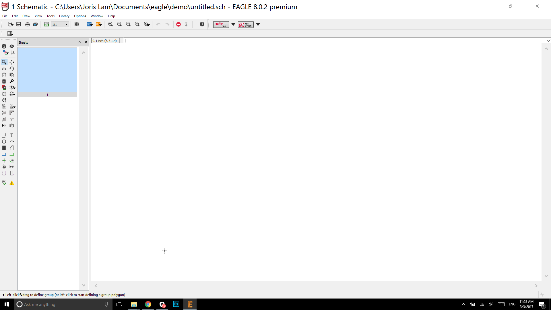
Now you will automatically go to the schematics window where you will design your schematics.
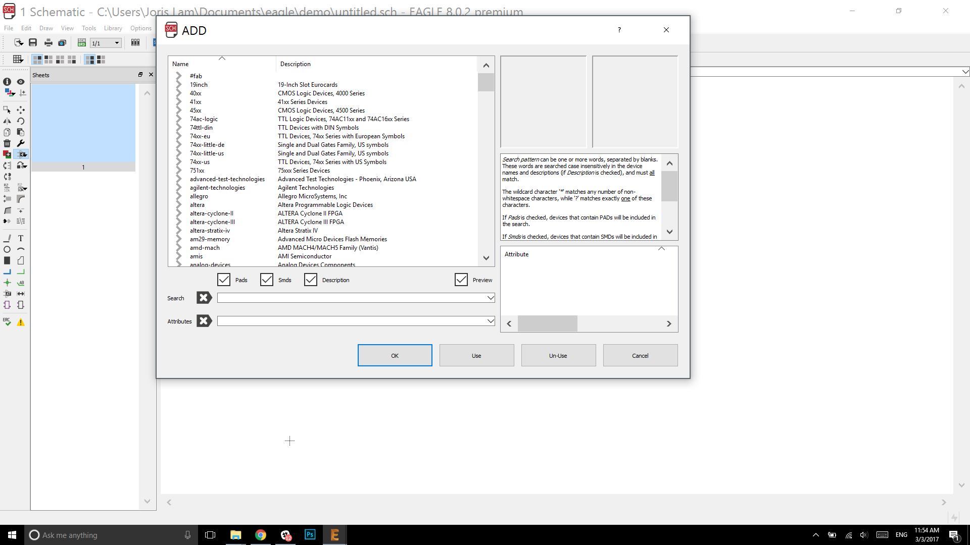
Start your schematic by adding components with this button on the left, and then choosing components from the window. Because I added a # to the file name the Fab library shows up on top.
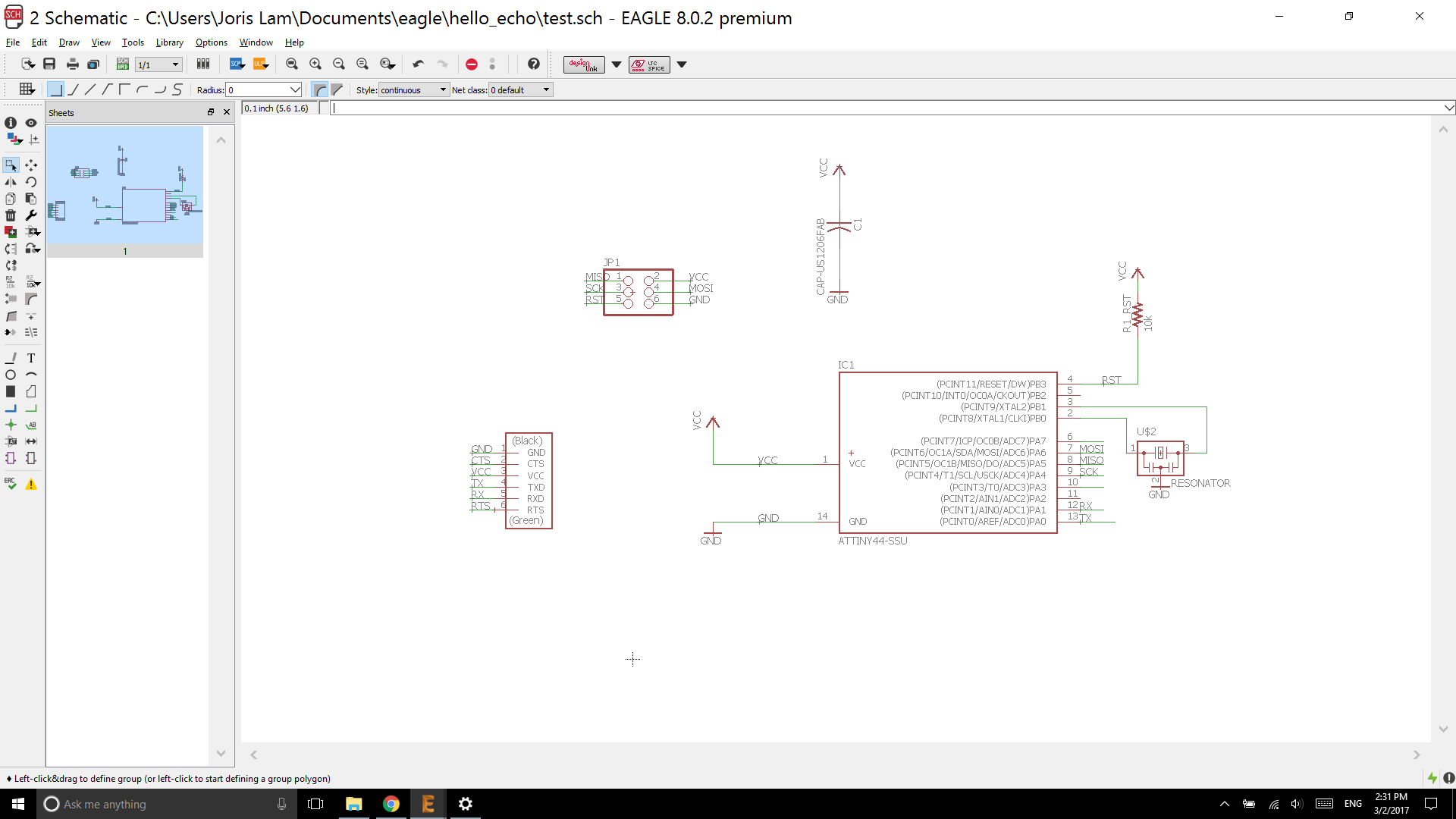
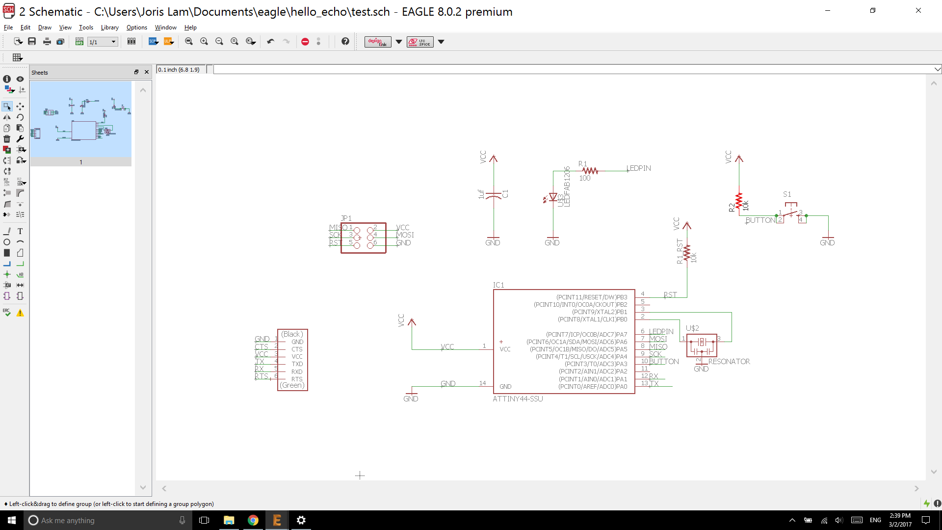
From this point just follow the tutorial mentioned above to redraw the schematics for the board. It should look something like this:
Then its time to add the button and LED, I chose for the same setup as the one in the tutorial, which turns the button into an input and the LED into an output using free pins on the microcontroller.
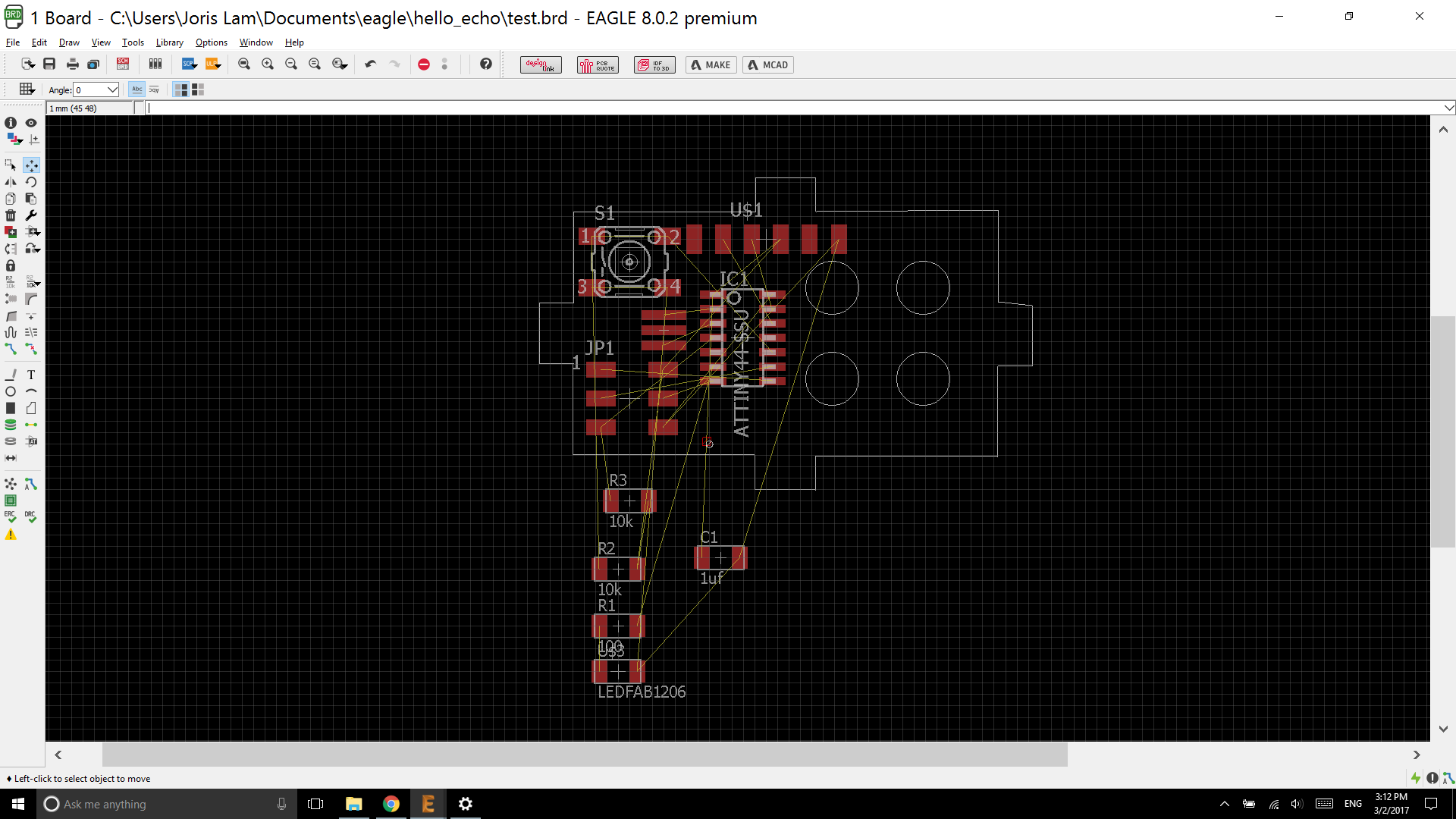
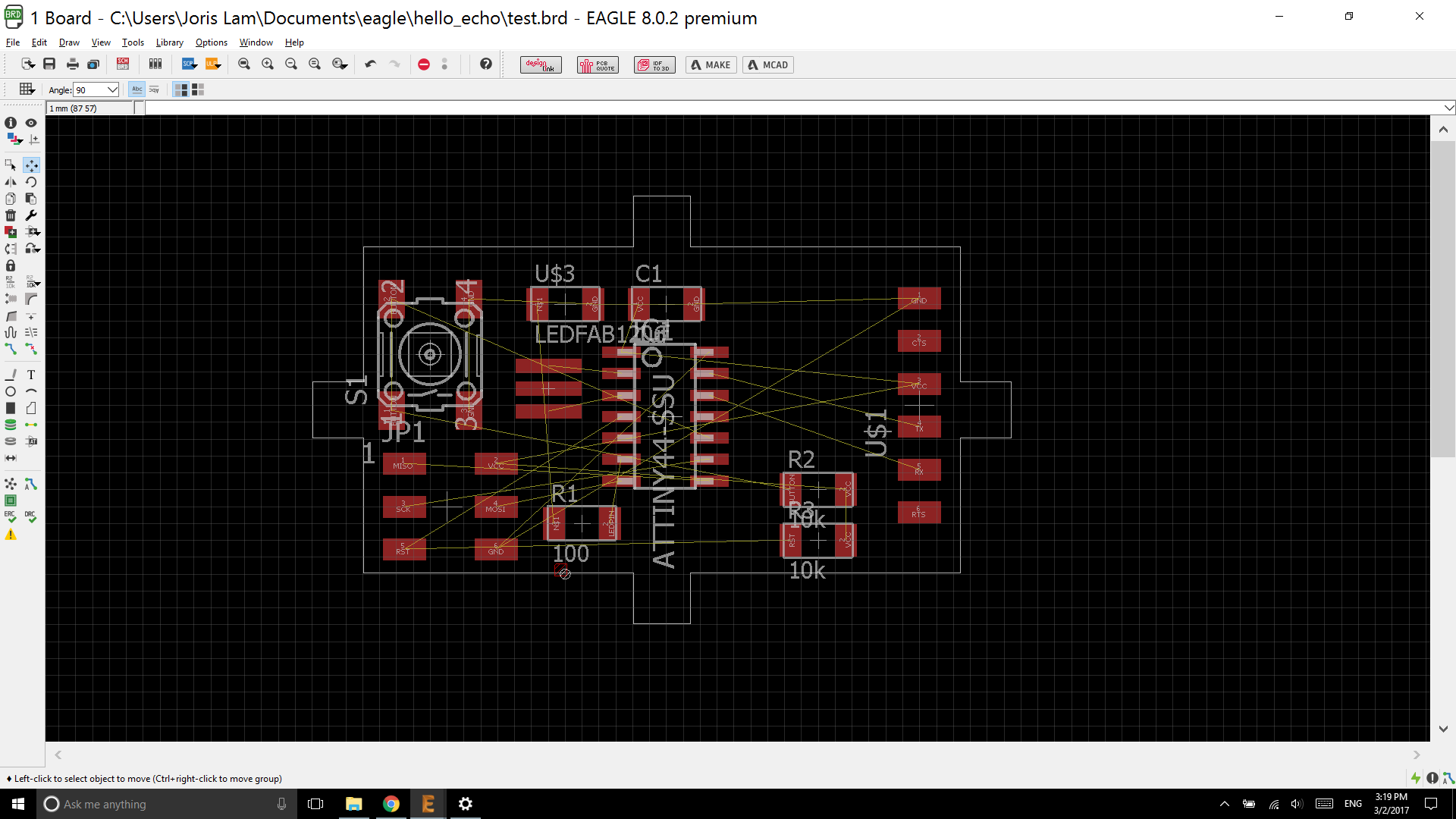
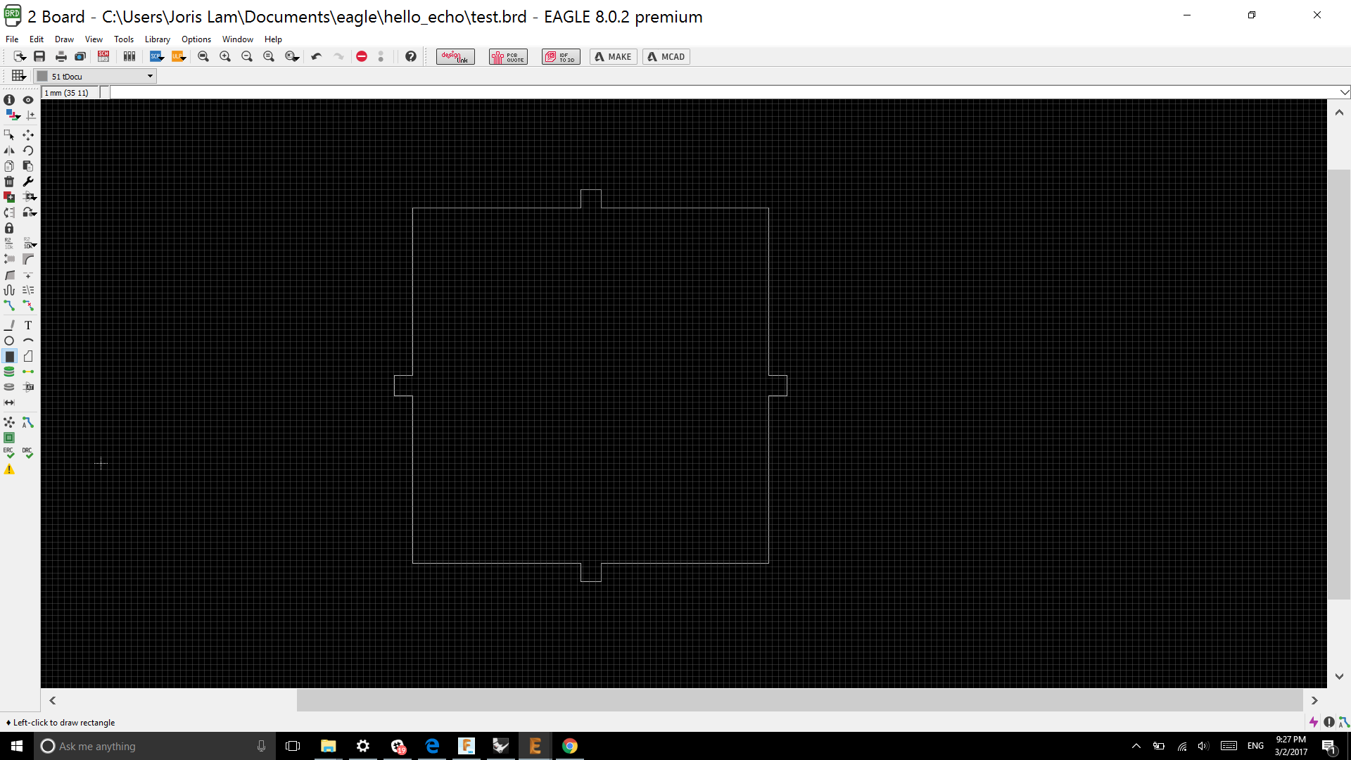
Now that the schematic is complete, you can switch to the board layout view, you do this by pressing the green icon in the top left of your screen. It should look something like this:
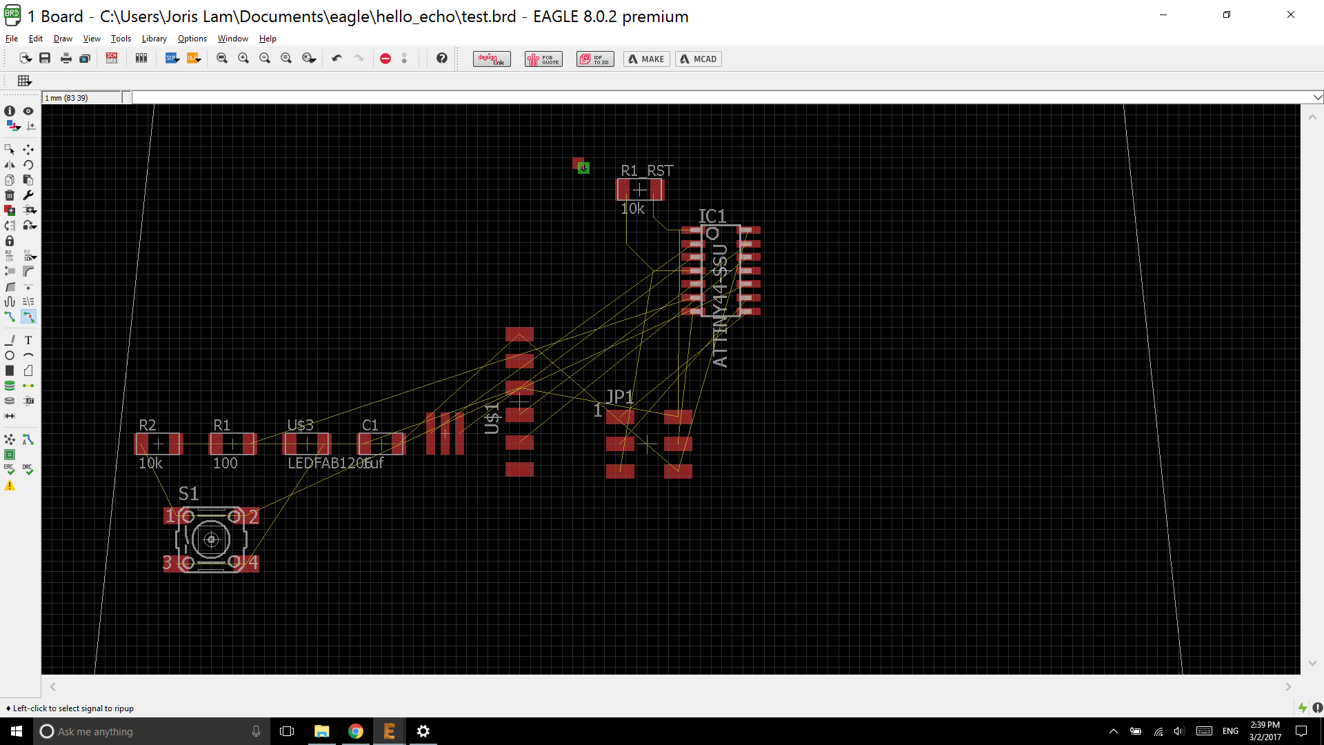
In the layout screen, there are yellow lines between components that are connected in the schematics. The next step is to place the components on a compact footprint that fits your board size and draw traces between the components that need to be connected.
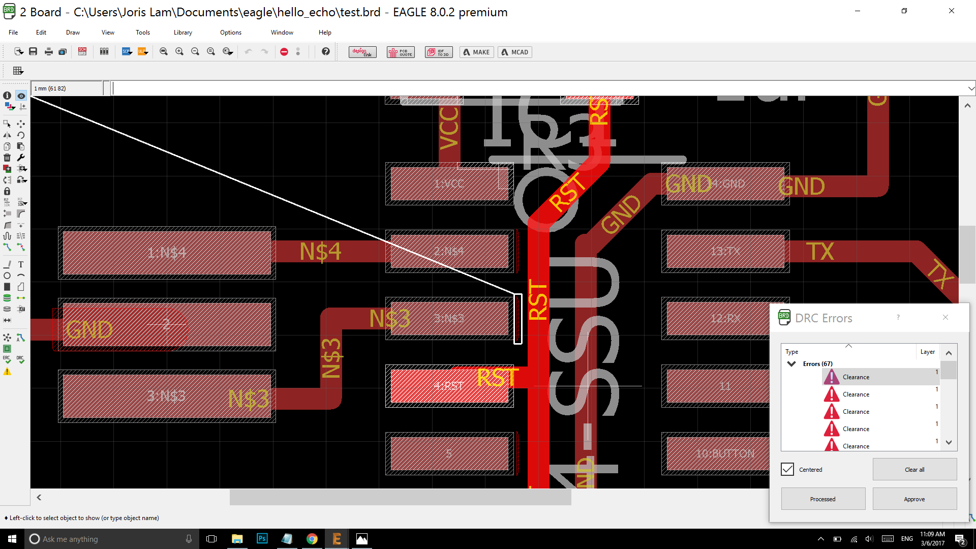
Before you start drawing, its a good idea to set some design rules, these can be specific to the board house you’re sending your design to, but in our case it involves the rules of milling.
The most important design rule to worry about now is the clearance of the traces, this should be set to 0.4mm.
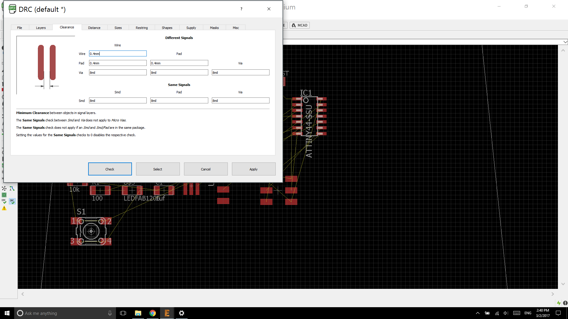
You can find the design rules under the ‘tools’ tab, then hit ‘DRC’.
For my final project I want to make an IoT sensorkit that is LEGO compatible, so I decided to see if I could fit this PCB together with the laser cut brick construction kit I made in week 03.
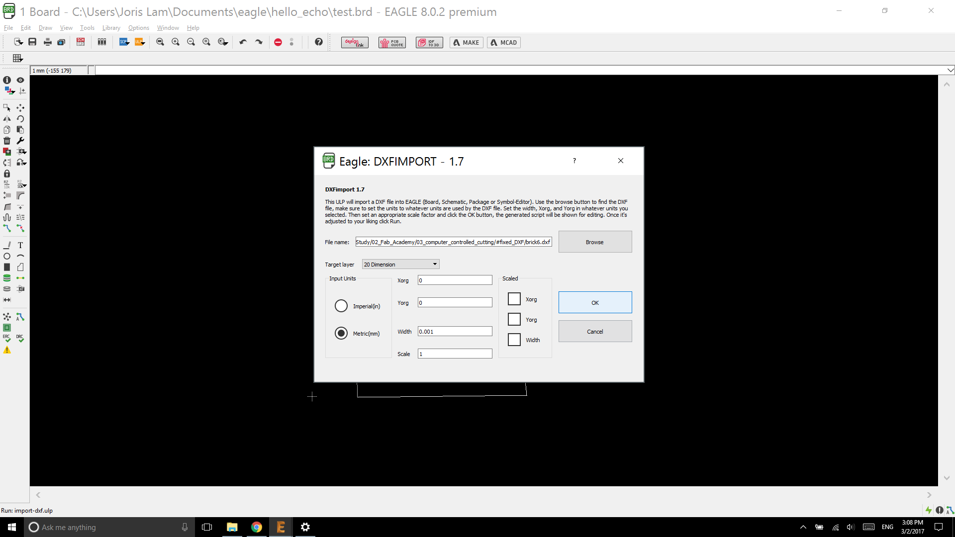
To see if I had any chance at all of fitting these components onto my original design, I imported the same DXF file that I used for the laser cutter, and tried to fit the components on it.
These are the import settings I used
And then it looked like this:
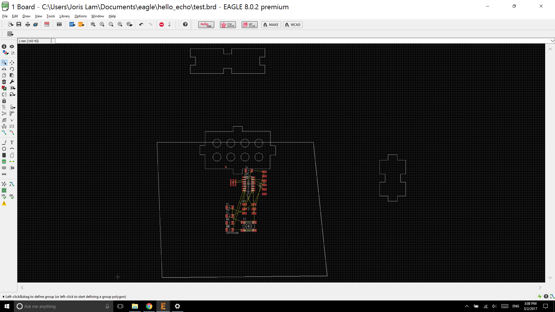
After cleaning up all the parts I don’t need I was left with the main part of the brick, and the challenge to fit everything on there, preferably keeping the holes too.
Ha. Well, no way this was ever going to work. Even without the holes, getting the components on there could work, but the traces with 0.4mm distance and just one layer was too big a puzzle for a first time Eagle user like myself.
I tried for hours finding a possible lay-out, but eventually I decided not to torture myself any longer, and just make a brick that is twice as big. By the time I get good at Eagle I can probably get the size down, but for now I’d have to make do with a bigger brick. Thankfully I designed the brick parametrically in Fusion 360, so making it bigger was a simple step. The steps I took and the file for the brick can be found here: http://archive.fabacademy.org/archives/2017/fablabamsterdam/students/60/03computercutting.html.
I made the layout according to the tutorial, in order to have a snug fit of all the components and traces, and after that I imported the new DXF.
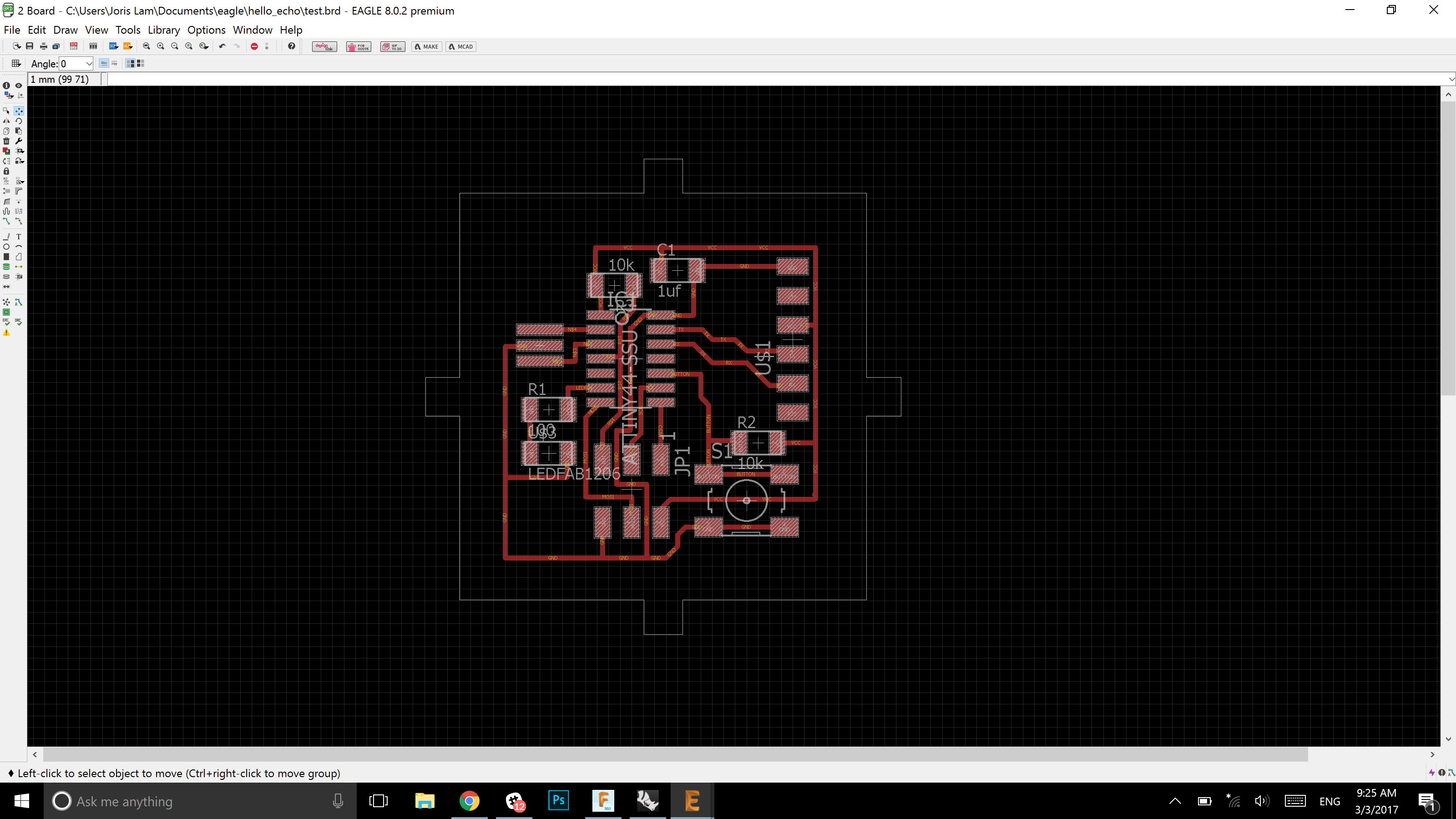
If everything looks good, use the ‘check’ function in ‘DRC’ under tools to see if there are any errors in your design that need attention. I did this, but when I thought I adjusted tolerances enough, I really didn’t. I didn’t address this tolerance error enough and it came back to bite me in the ass later.
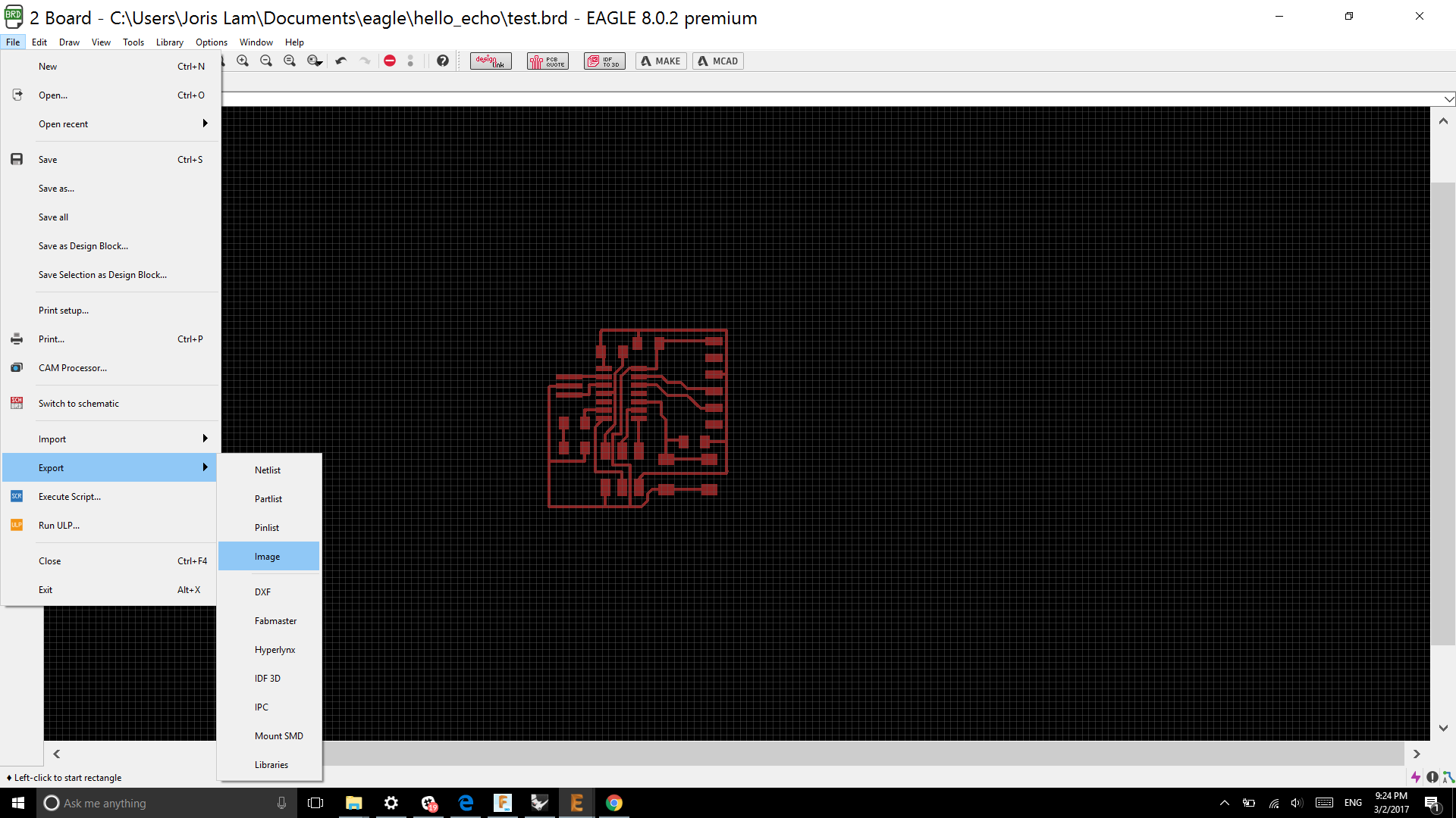
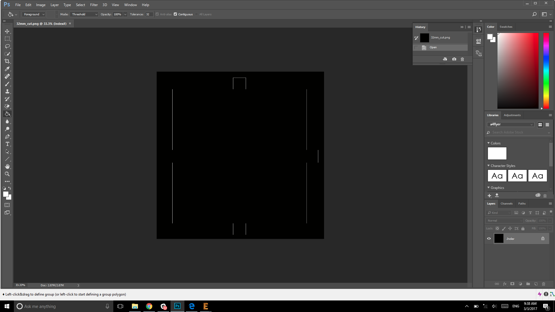
To make PNG’s that can be read by Fab Mods, I followed these steps:
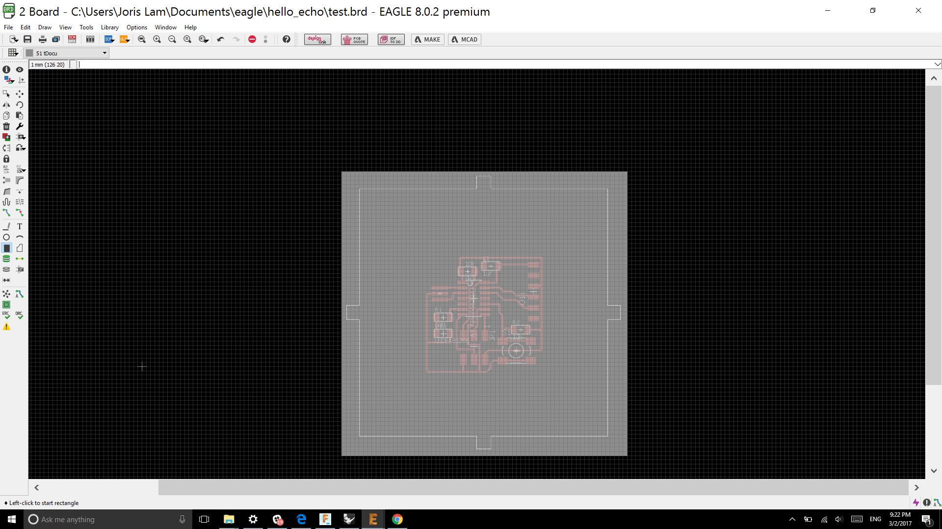
First, draw a rectangle around the outline of your board, and place it in an unused layer, for instance layer 51.
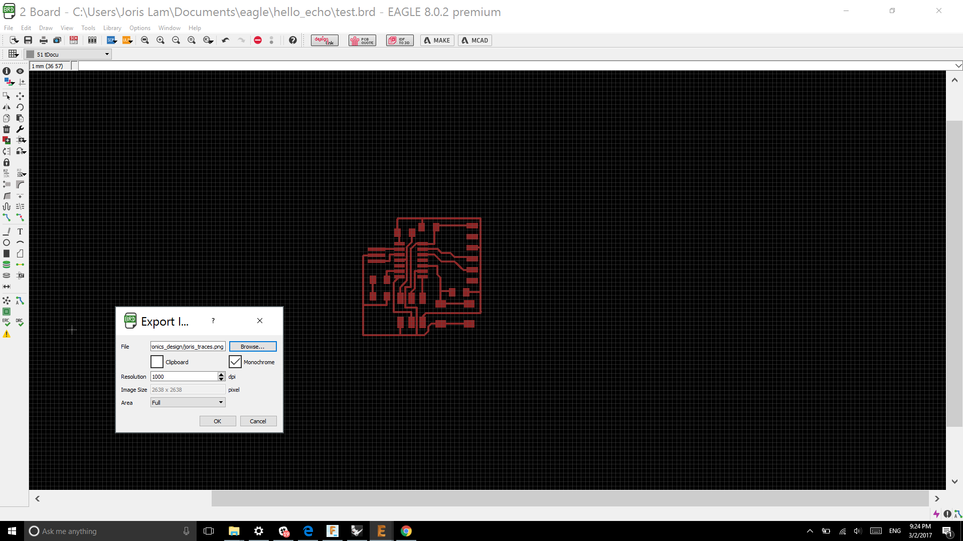
Then, deselect all layers from the view, except for the traces and pads, and export to ‘image’.
Choose the following export settings.
Repeat the steps, but this time, just leave the cut line visible.
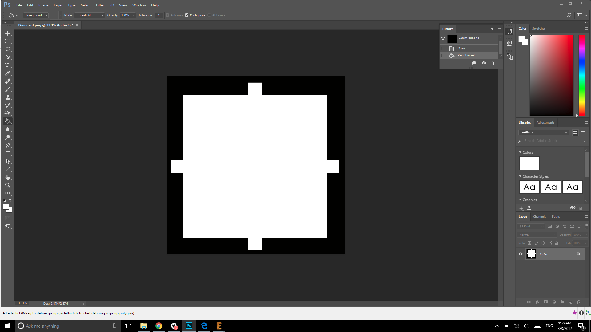
The cut line PNG needs one more action, which is making the inside white, to do this, I opened the PNG in Photoshop:
And I used the paint bucket to make the inside white, then saving it with the original settings.
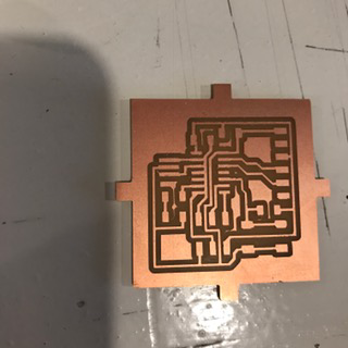
After this the files are ready to be milled, for the milling, I followed the steps described in week 04.
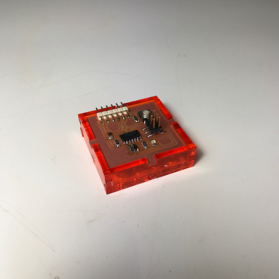
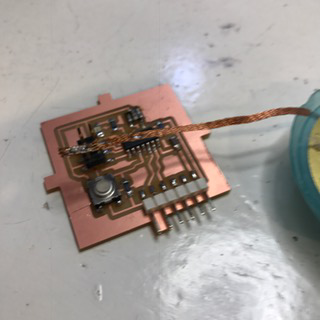
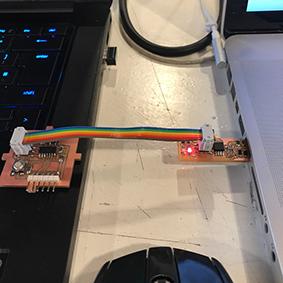
The board came out looking like this:
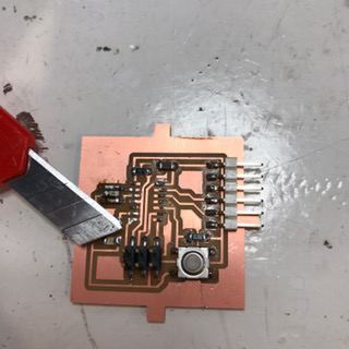
I thought nothing was wrong with it, so I went ahead and soldered it. That was a bit of a mistake as one side of the IC legs was completely shorted. I only found out about this after all the soldering was done, so I had to remove the ATtiny. To do this, first I used solder braid to remove the most of the solder and then I used a heat gun to remove it completely.
Then I used a knife to cut the traces that should not have been connected, and I used a multimeter to check if the connections really had been broken.
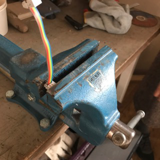
After the mistake had been fixed I made a connector from a ribbon cable to connect the new board to the ISP.
I took six cables out of the nine, and put them in a special connector.
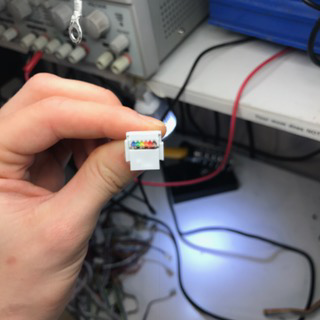
To close the connector I gave it a gentle push in the woodworkshop.
PROGRAMMING THE BOARD
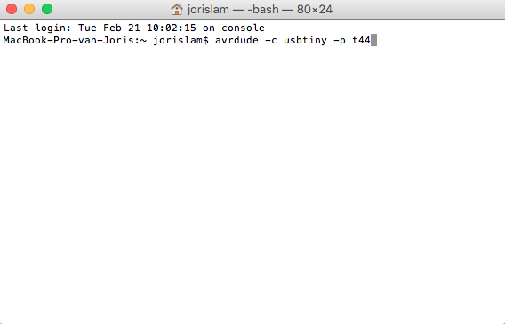
I did this on a Mac, to program the new board I opened the terminal as I already had avrdude installed from week 04.
In the terminal, I gave this command:
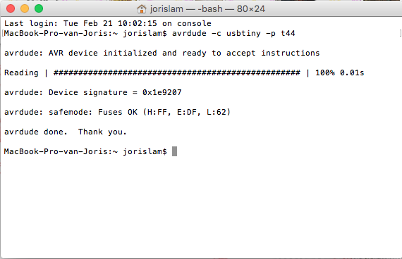
And I got this back, meaning the board works and communication is running smoothly.
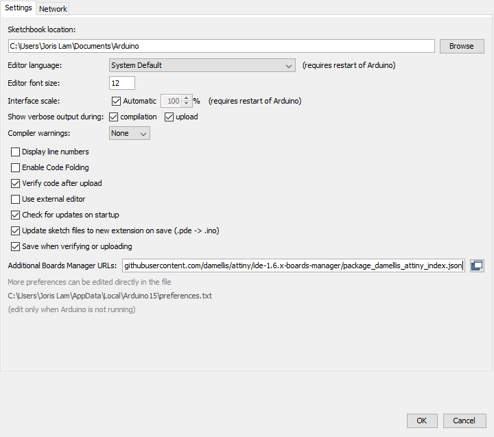
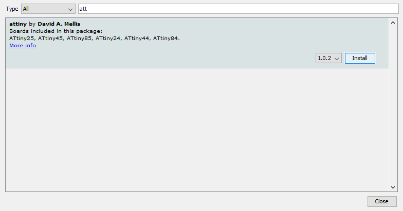
To program it, I used the Arduino IDE, but in order for this to work, you need to add the Attiny44 as a board. To do this, follow these steps:
1 - under ‘preferences’ under the ‘additional boards manager’ add this URL:
https://raw.githubusercontent.com/damellis/attiny/ide-1.6.x-boards-manager/package_damellis_attiny_index.json
2 - Under ‘tools’ go to ‘boards’ and ‘board manager’, if you type ‘attiny’ in the search bar, you will now see the board which you can install.
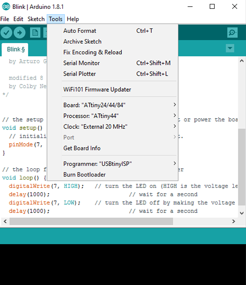
3 - Now you can burn the bootloader onto the ATtiny, make sure that under ‘tools’ you set all of these settings correct, and then hit ‘burn bootloader’.
4 - To test if I could upload and run a program, I used the simple ‘blink’ sketch from the examples built into the IDE, and changed the output to PIN 7.
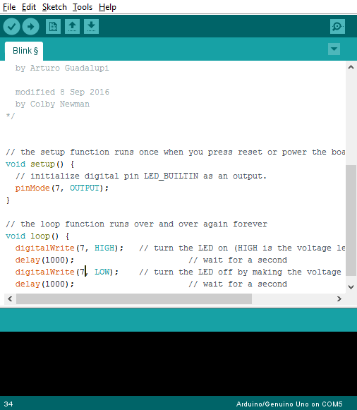
5 - After uploading the sketch it worked! The LED was blinking.
FINAL RESULT
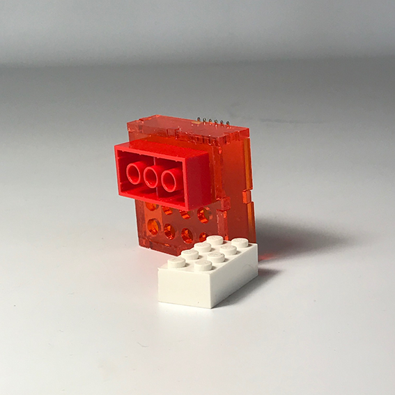
To make this board LEGO compatible, I laser cut a fitting casing, based on the parametric design from the computer cutting week. Assembled it looks like this:
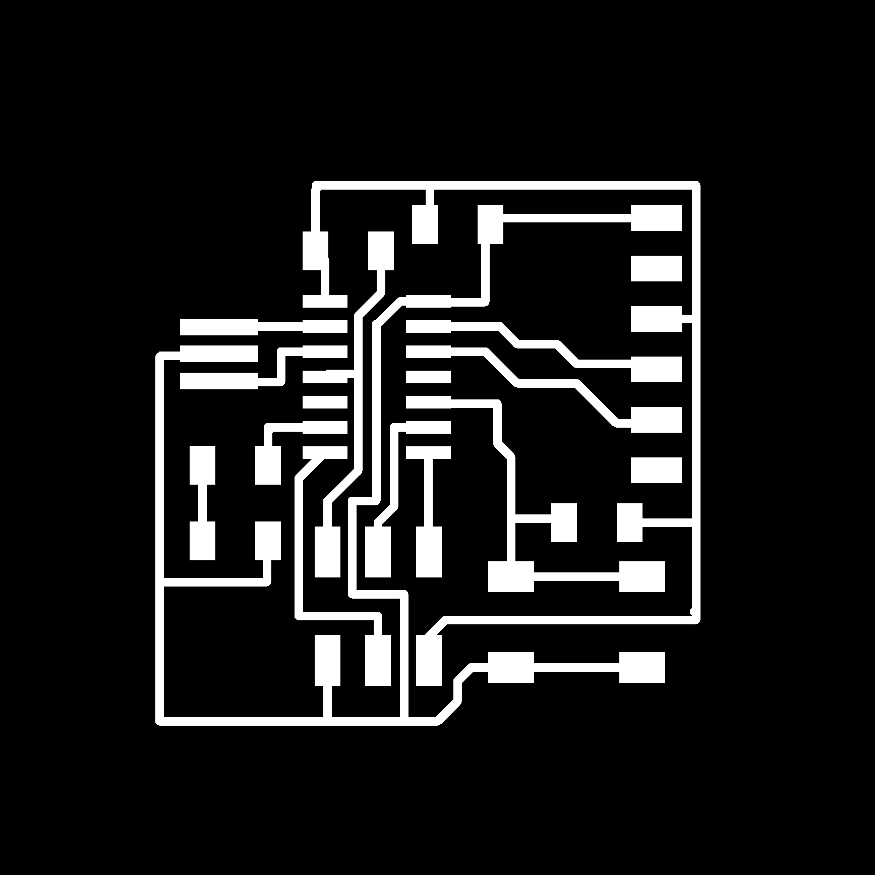
traces PNG
outline PNG

schematic Eagle
board layout Eagle