Week #6 ELECTRONIC DESIGN
Assignment
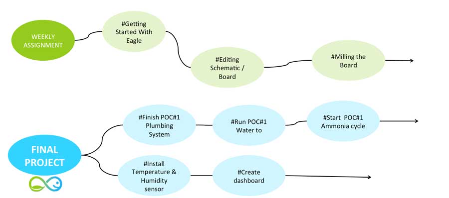
Week workflow
This is how I see my week
Softwares used
- Eagle
- GIMP
- Fab Modules
Eagle
Getting Started With Eagle
EAGLE (Easily Applicable Graphical Layout Editor) is a flexible and expandable EDA schematic capture, PCB layout, autorouter and CAM program. EAGLE is popular among hobbyists because of its freeware license and rich availability of component libraries on the web. We will use Eagle to layout and modify a circuit board for this assignment.
To get familiar with EAGLE, I started by watching the following tutorials on Youtube and read the one that we got in Fab Academy
Edit the Schematic
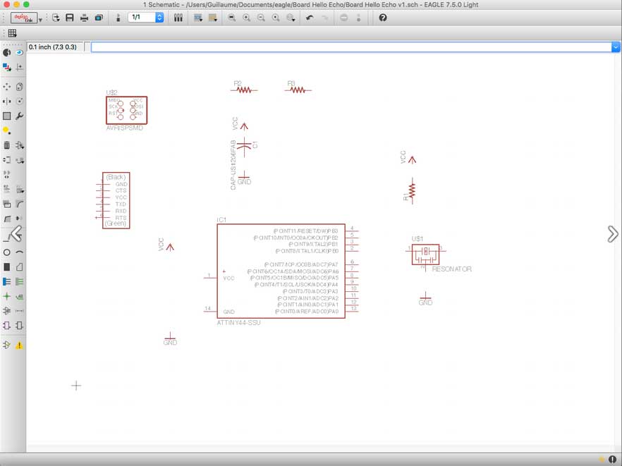
First thing I did, was to redraw the design schematic from Neil "hello World" board following the Week6 - Introduction Tutorial to EAGLE adding the following components:
- 6-pin programming header: for programming the board
- microcontroller: attiny44A: Once the microcontroller is programmed, the program stored in non-volatile memory. This means that it will remember the program.
- FTDI headerpowers the board and allows board to talk to computer
- 20MHz resonator: external clock. The attiny has a 8Mhz clock but the resonator is faster (increase the clock speed of the processor) and more accurate.
Add / Connect Components in the Schematic
To add a component, you can either type "add" or select the "add icon from the toolbar". The add menu will open. You can either look through the listed libaries for a component to add or you can type it into the box above the "drop" button.
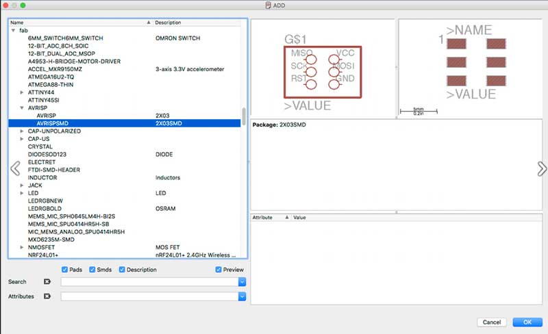
I've followed the same procedure with the others components
To connect components in the schematic, I've used two different ways:
- You can connect the components with a wire (also called a "net" in Eagle). This may make connections obvious at first, but can get really messy quickly as nets cross over each other.
- You can also name the nets attached to components that need to be connected by naming them with the same name. Eagle will ask you if you want them to be connected. (Say yes!). After you name the component - label it so the name appears in the diagram.
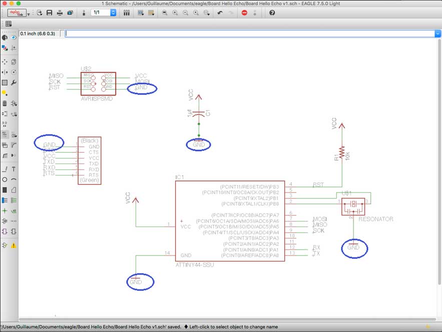
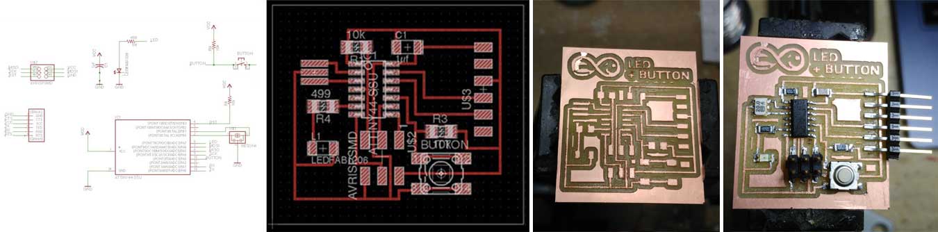
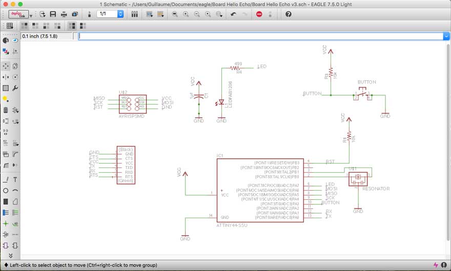
This is the resulting schematic.
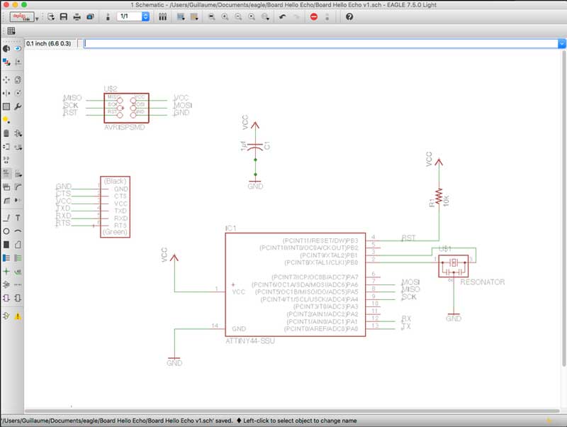
Add / Connect LED + Button components in the Schematic
On the top of Neil board schematic, we had to add / connect the extra following components following the same process as described before:
- Resistor(value 10k)
- Button(OMERON switch)
- Ground
- VCC.
- connect pin 10 (PA3)on the microcontroller to the button LED (Light Emitting Diode) - LEDs have polarity - the side with the line is the cathode and connects to the ground side.(see schematic below)
- Resistor(value 499 ohms)
Route the Traces on the Board
Once you have the schematic, switch to the board view
- Go to the top menu > File > switch to board
- The board view will open up
- The components you just added will be jumbled up in a corner with yellow unrouted traces attached.
Use "move" to move each individual component around.
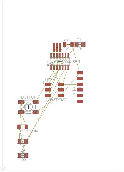
Once placed components, there are few features to understand before tracing the routes
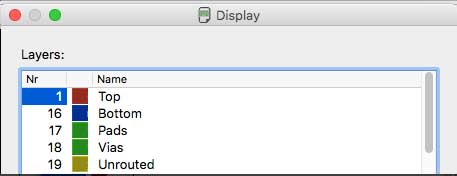
Understanding Layers settings
There are a lot, but it is not important to understand all of them but let's talk about the important ones.
- "Top" defines the top coppers layer, this is where you wanna have connection between various components.
- "The Bottom" is when you have copper at the bottom of the board, but in our case it is not the case
- "Pads" and "vias" will define the connections we have between the Top and Bottom layer
- "UnRouted" are the yellow wire we need to route
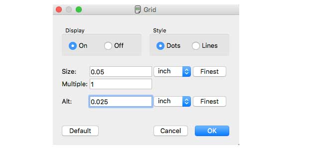
Understanding GRID settings
In the schematic editor we never even looked at the grid, but in the board editor it becomes much more important. As EAGLE forces your parts, traces, and other objects to “snap” to the grid defined in the Size box, it is good to know that you can adjust the granularity of the grid, by clicking on the GRID icon.
If you need finer control, hold down ALT on your keyboard to access the alternate grid, which is defined in the Alt box.
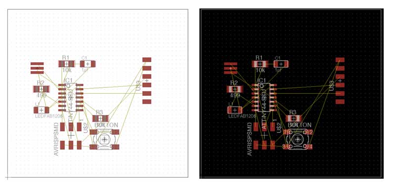
Change BACKGROUND settings
Having a Black background is more convenient to edit the board
Change NET settings
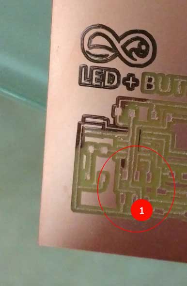
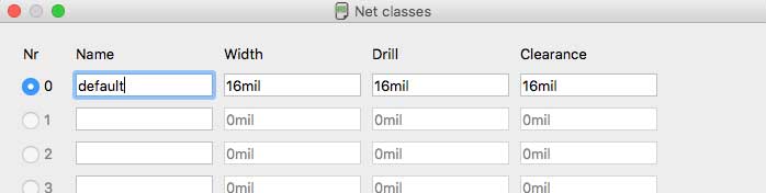
The above picture shows very tiny traces on my circuit board. The reason is during my first attempt to mill the board, I didn't pay attention to the default presets associated to the width of vias on Eagle.
In Eagle you can associate a class with a net. The class defines some information to control the width, clearance and drill of vias. By creating a specific class for the ground, the power supply and normal signals, we can control quite easily the width of each signal. The feature is quite hidden in Eagle and I think it is not well explained. First, in the Eagle board editor, activate the class editor.
To fix that, I went to:
Edit / Net Classes / Nr 0 (which is the class associate to the vias) / Change default values from "8 mil " to "16 mil" everywhere
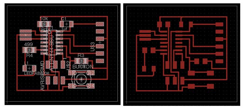
Ready to route the traces
To route the traces, you can either do it manually or do it automatically with the "autorouter" option. I decided to do it manually.
Checking for Errors
Before we package the design up and send it off to the Roland MDX, we can use to check our design for errors:
- Ratsnest – Nothing To Do!The first check is to make sure you’ve actually routed all of the nets in your schematic. To do this, hit the RATSNEST icon – – and then immediately check the bottom left status box. If you’ve routed everything, it should say “Ratsnest: Nothing to do!”
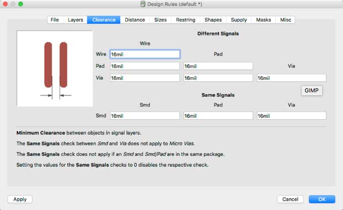
- Design Rule Check: Once you’re done routing there’s just one more check to be made: the design rule check (DRC). For this step, put in all the fields of clearance at "16 mil value" because it corresponds to the thickness of our milling 1/64 bits. I press "Check"
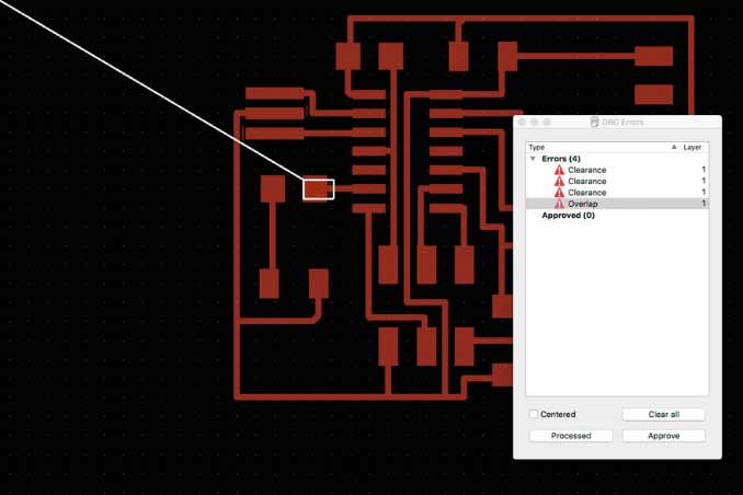
DRC sent me back 4 errors
- 3 Clearance because I had traces too close to either another trace or a via. To fix this, I nudged the trace around using the MOVE tool.
- 1 Overlap because two different signal traces were overlapping each other. It would have been created a shortcut if not fixed. I had to RIPUP the trace, and try routing it on the other side of the board.
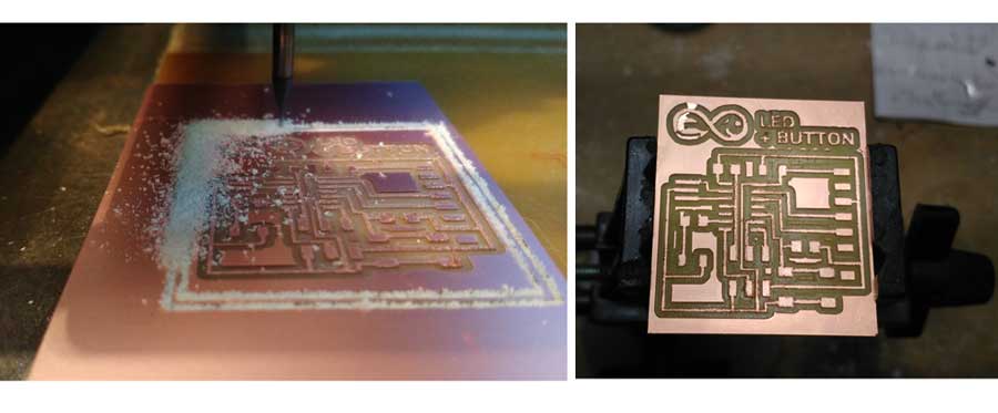
Once you’ve seen both “No airwires left!” and “DRC: No errors.”, your board is ready to send to the fab house, which means it’s time to generate some gerber files.
Exporting the Board Design to be Used with Modela
To prep board for milling:
- In layers menu in the top toolbar, select the only the top layer (traces only)
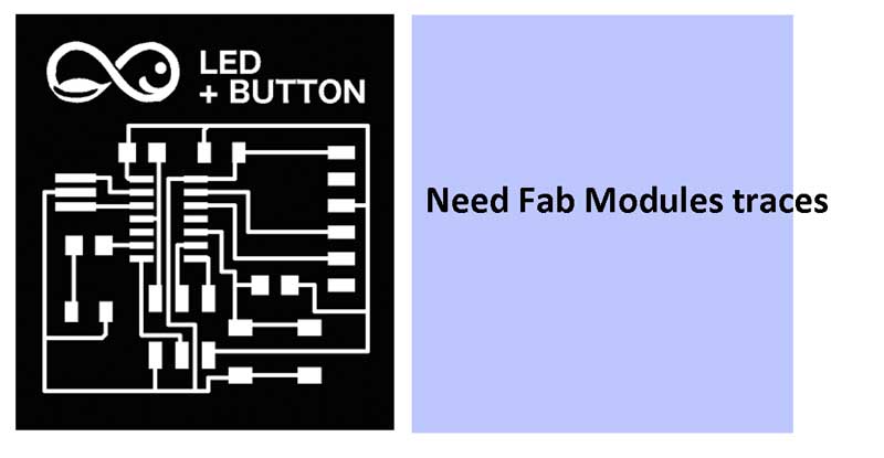
- then export as a png (file -- export -- image)
- settings should be MONOCHROME and 500 DPI - this will export a image with white traces.
I've used GIMP to edit the board files and create the traces and mill-out files.
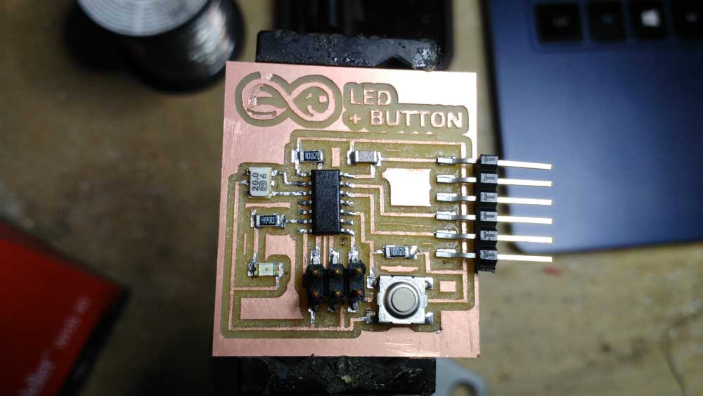
Welding the board
This board is not very difficult to weld, the chip is large enough to be welded with a low power welder seamlessly, maybe the most complicated piece for soldering is the resonator, to facilitate welding of this part, it is best to use a little FLUX.
Final Project evolution
Download
You access and download all the files generated during this week from my google drive:
Conclusion
I was completely new to Electronic design and it has been a great introduction week. One of the great learning of this week is about the settings you need to take care (i.e. grid settings, net settings ) before starting editing the traces on the board. What's more, it is essential to adapt the Design Rules according to your local machine / tools and check if DRC are all respected before exporting your your file.