Electronics Production
Overview
Last updated: 07/03/2016
Objective Make the Fab (tiny)ISP in-circuit programmer. Learning outcomes 1.Describe the process of production; 2.Demonstrate correct workflows and identify areas for improvement if required; Have I... Shown how I made and programmed the board? Explained any problem and how I fixed them? Included a hero shot of my board? Summary This week consisted of producing a programming board, in particular the FabISP. In this page I explain the process I went through: milling the PCB, soldering the components, designing the case and eventually programming the microcontroller. Unfortunately, my week went not that smooth, so I also explain the struggles I had in actually getting the PCB to work. In particular, the redesign chapter also includes the explorations that I did with producing PCB with both the laser cutter and the vinyl cutter.FabISP FabISP is a programmer that allows for loading code on AVR microcontrollers (e.g. ATtiny, ATmega). The FabISP is based on Dick Streefland's USBTiny who put together a clear explanation of what the programmer is and what it is used for. We choose v2.3, which contains a cristal timer and has the USB hardware architecture.
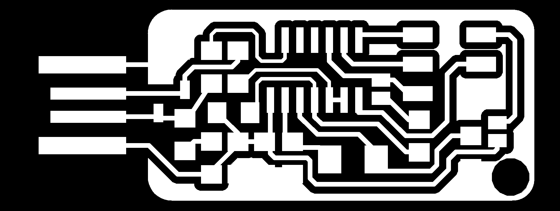
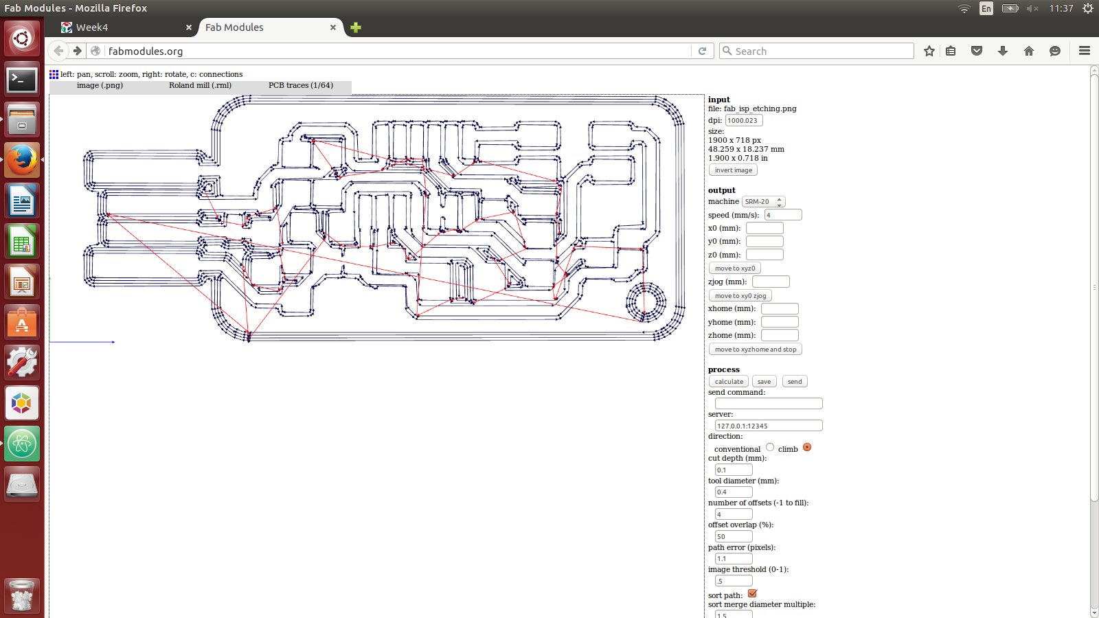
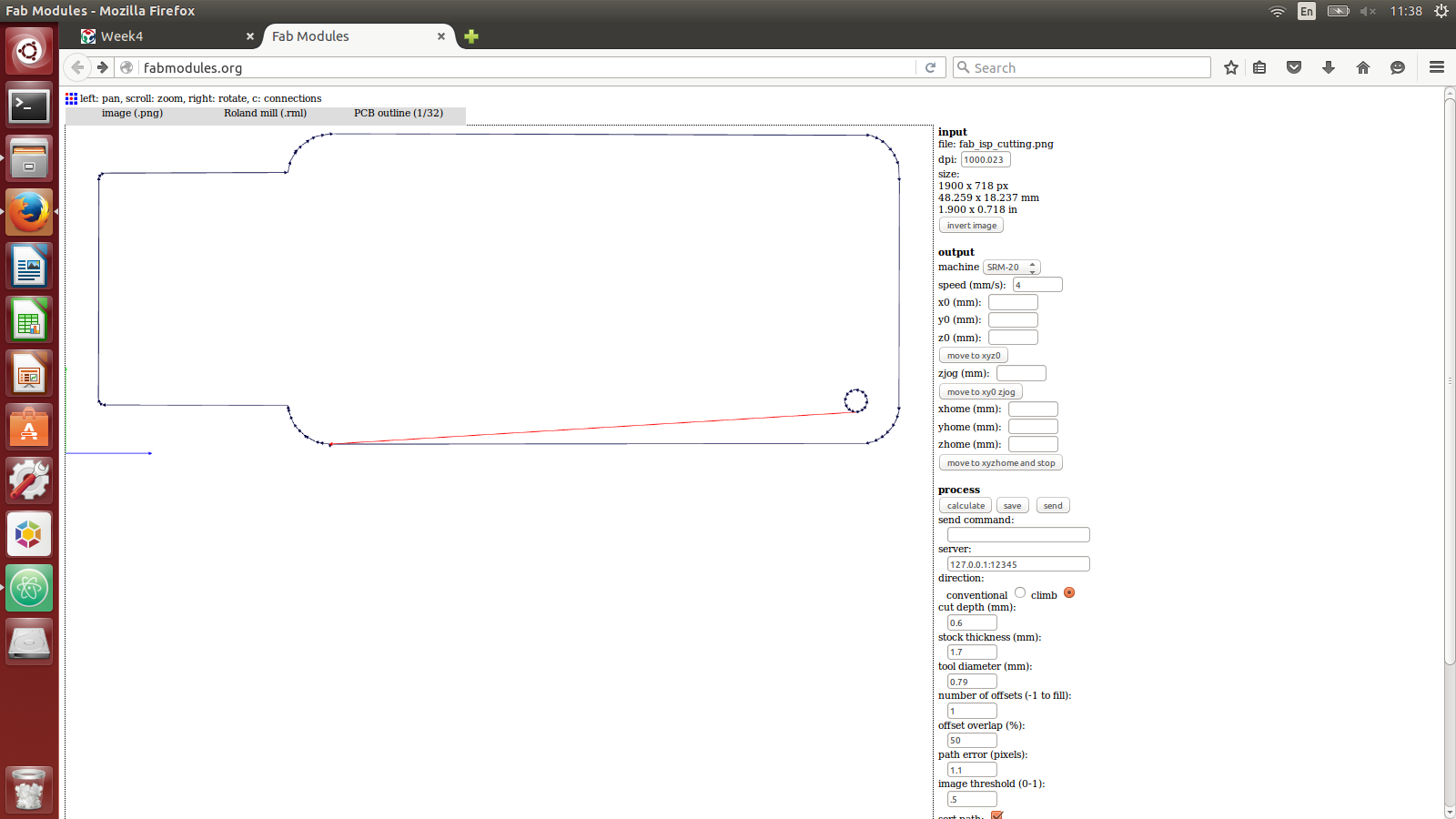
Milling the circuit In Siena we have a Roland SRM-20. The printplate we soldered is made out of phenolic paper, which is a fairly little toxic material to machine. In the following I explain the steps of machining the pcb, starting from .png files of the circuit to be produced. 1.Gather the drawing of both the etching and the cutting as two separate .png files [1], [2];

 4.Carefully tape the board to the base of the machine;
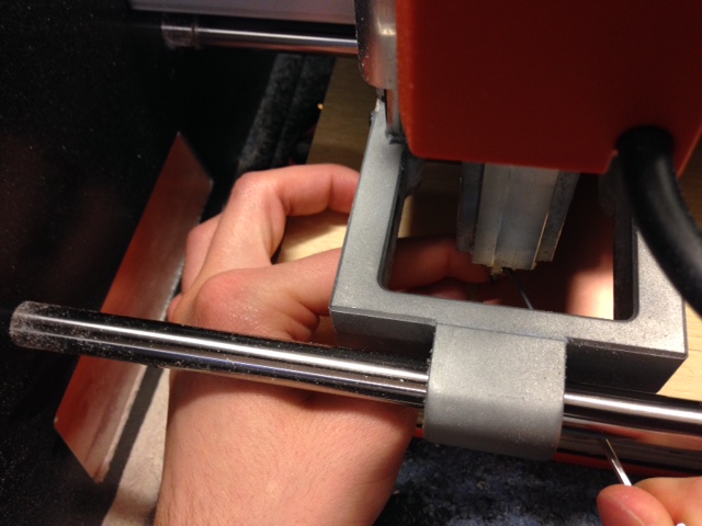
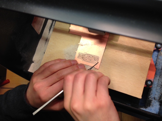
5.Manually install the first drill bit (1/64 of an inch) which is used for etching only. This is a careful operation, as show in the picture below.
4.Carefully tape the board to the base of the machine;
5.Manually install the first drill bit (1/64 of an inch) which is used for etching only. This is a careful operation, as show in the picture below.
 7.Launch the first work. While executing, check that it makes dust, because it should;
8.Prepare the second file and keep the standard settings (Roland Mill, PCB outline 1/32). In this case, one offset is enough;
7.Launch the first work. While executing, check that it makes dust, because it should;
8.Prepare the second file and keep the standard settings (Roland Mill, PCB outline 1/32). In this case, one offset is enough;
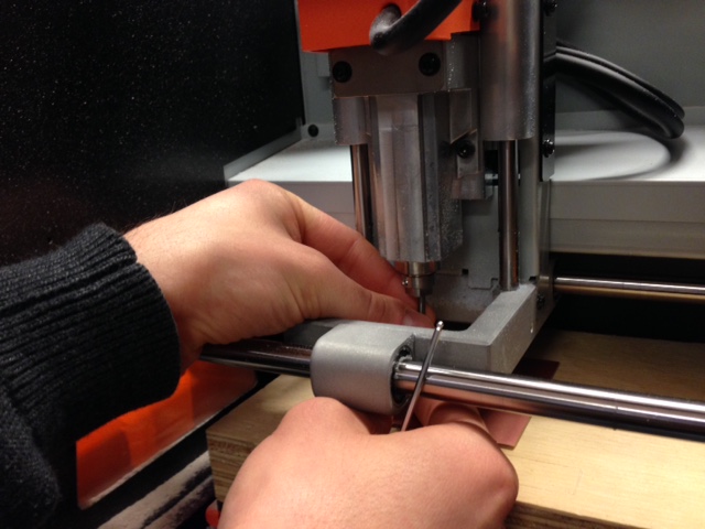
 9.In the same way as before, mount the second drill bit (1/32 of an inch) which is used for cutting only;
10.Re-set the Z axis;
11.Launch the second work;
12.Gently take the board out;
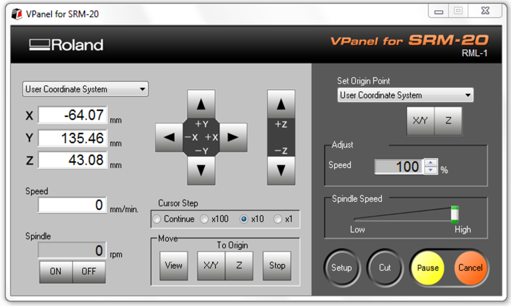
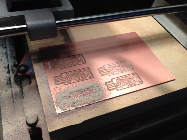
After that, we started to "mass-produce" boards. In order to optimize the process we did first do all the etching and we later did the milling. By setting the options to "Machine Coordinate System" you can read and store somewhere the coordinates for repeating the jobs later with the other drillbit. Again, the interface is not super-friendly as it does not allow you to manually insert values.
9.In the same way as before, mount the second drill bit (1/32 of an inch) which is used for cutting only;
10.Re-set the Z axis;
11.Launch the second work;
12.Gently take the board out;
After that, we started to "mass-produce" boards. In order to optimize the process we did first do all the etching and we later did the milling. By setting the options to "Machine Coordinate System" you can read and store somewhere the coordinates for repeating the jobs later with the other drillbit. Again, the interface is not super-friendly as it does not allow you to manually insert values.
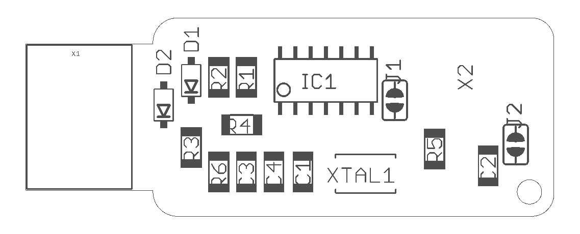
Gathering the components Even though in this case it was already arranged by our tutor, a normal workflow would involve finding (perhaps buying) the components for the board. Sellers are DigiKey (cheaper but with longer delivery time) or RS-Online (more expensive but they deliver in 24h). We used SMT components, which seemed a bit challenging to find. The components used for producing this board are:
| Amount | Component | Schematic | RS-code |
|---|---|---|---|
| 1 | Quartz 20 MHz | XTAL1 | 811-7878 |
| 1 | ATTiny 44 | IC1 | 696-251 |
| 2 | 49,9 Ohm | R1, R2 | 223-2120 |
| 1 | 1K Ohm | R3 | 223-2265 |
| 1 | 10K Ohm | R4 | 223-2394 |
| 1 | 0 Ohm | R5 | 679-1768 |
| 1 | 499 Ohm | R6 | 679-2171 |
| 2 | Zener 3.3V | D1, D2 | 687-8250 |
| 2 | 10pF | C1, C2 | 461-4063 |
| 1 | 100nF | C3 | 723-6593 |
| 1 | 1 microF | C4 | 766-1062 |
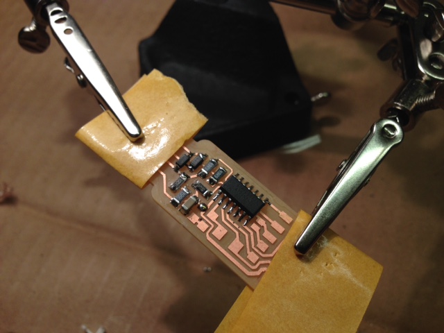
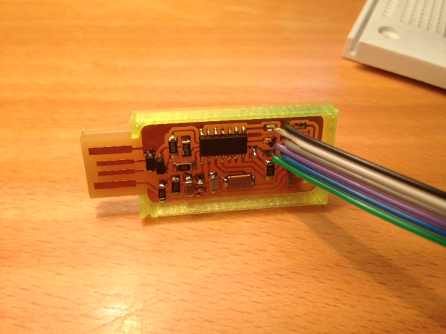
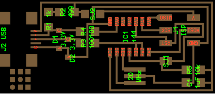
Soldering In this section I put together a list of tips and tricks that I learned when soldering: 1.Soldering should be done at 350-370 degrees, even though it is always better to check the datasheets of the components to make sure not to fry anything; 2.The order of soldering should be from inside to outside; 3.The order of soldering should be from small to big parts; When soldering the board I looked at the schematic below.
 The steps I followed are the following:
1.Melt some tin on the pad of the pcb;
2.Place the component and stick it on the one side;
4.Rouoghly solder it;
5.Solder with some tin the other pin, leaving the iron there 8-10 seconds;
6.Heat again the first pin, on order to obtain a shine-smooth surface;
The steps I followed are the following:
1.Melt some tin on the pad of the pcb;
2.Place the component and stick it on the one side;
4.Rouoghly solder it;
5.Solder with some tin the other pin, leaving the iron there 8-10 seconds;
6.Heat again the first pin, on order to obtain a shine-smooth surface;
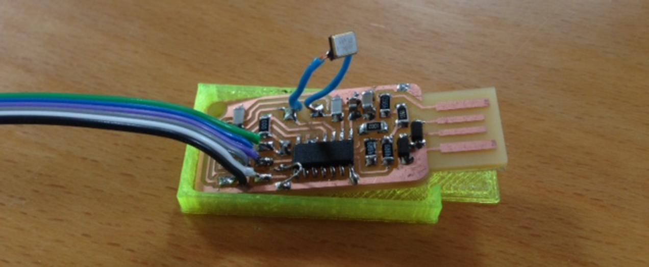
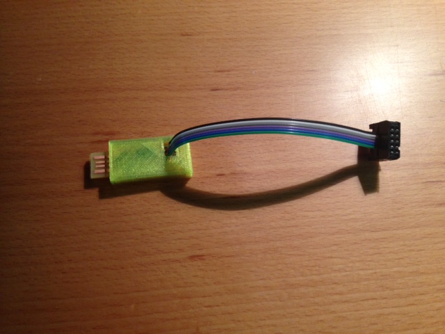
Case design First I started with this tutorial that clearly explains how to 3D print a plate to fix under the board in order to achieve perfect fitting with a USB port. Following the tips of Nickolas I found out that the optimal thickness for the casing would be 0.5mm. From his own sketches I just modified a bit the dimension of the top hole [3].
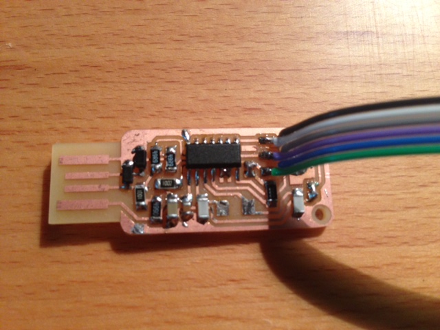
Programming Since we did not have another FabISP to programm ours, we used an Arduino Uno as an AVR-ISP to upload the registers on our own FabISP. There were a couple of websites we looked at, such as the work of Giacomo and this tutorial. Eventually Instructables seemed very clear. I followed these steps: 1.Make sure that Arduino IDE is up-to-date and upload the ArduinoISP sketch to the board; 2.Connect the two boards according to the schematic below;
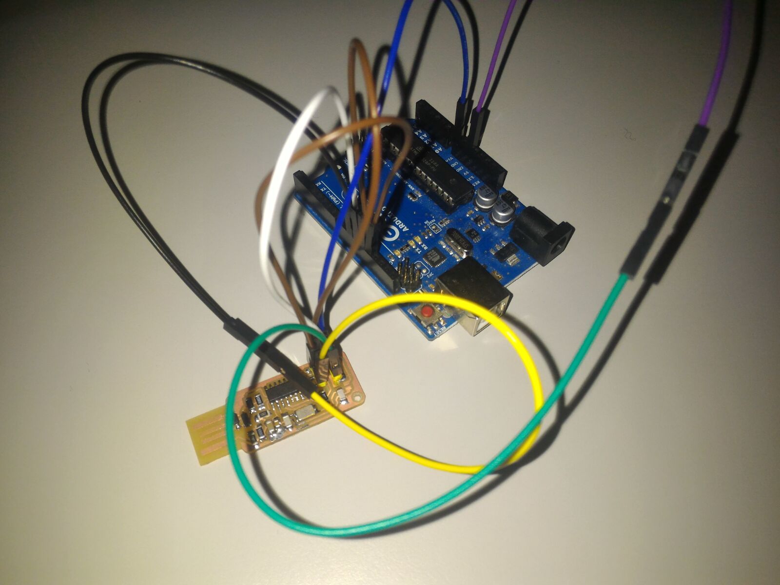
#AVRDUDE = avrdude -c usbtiny -p $(DEVICE) # comment this line
AVRDUDE = avrdude -c arduino -b19200 -P /dev/ttyACM0 -p $(DEVICE)make clean
make hex
sudo make fuse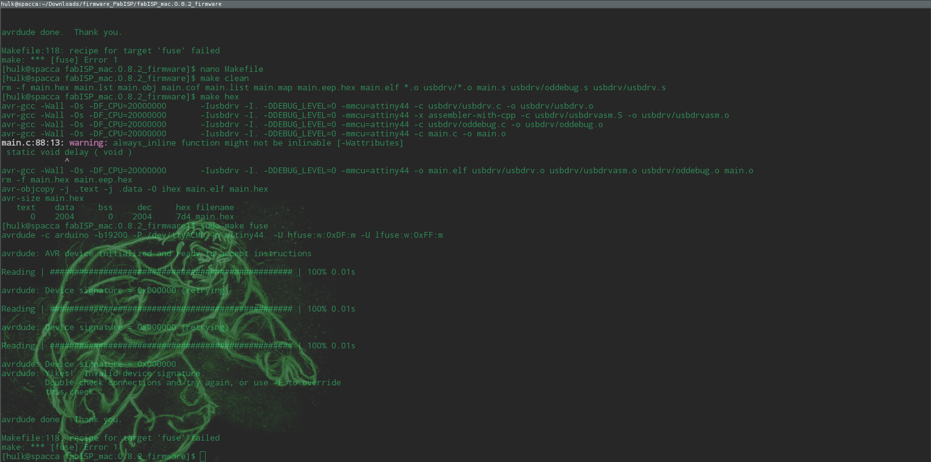
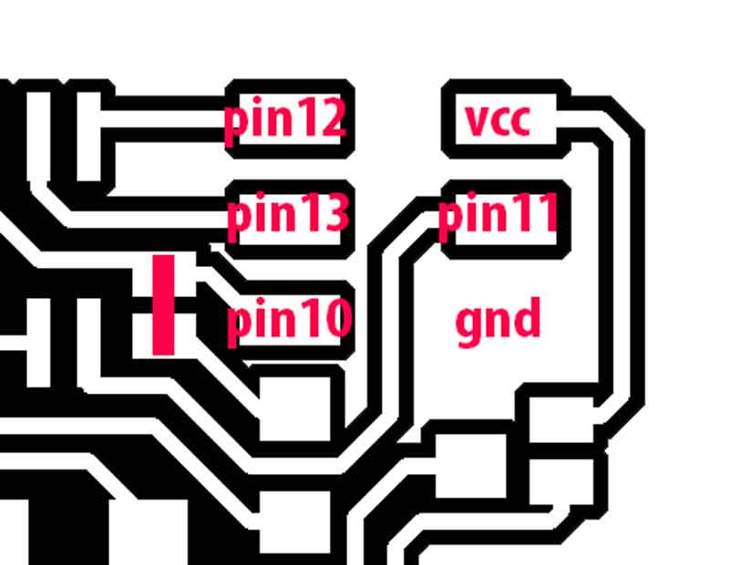
Debugging process I started to thoroughly check all the hardware connections, since I knew that the software implementation was correct, as it worked on the board of my colleagues. With the multimeter I tested a couple of things: 1.Resistor values, to make sure I placed them correctly; 2.Diodes flow, to make sure I did not invert the polarity;
3.If the board was actually alimented with 5V; Overall, I could not really find any evident mistake, which was kind of really frustrating. This tutorial quite nicely puts together what the most common mistakes can be when soldering. It seems that a common mistake with surface mount components is the insufficient wetting of the pad, which happens when you heat the pin instead of the pad. However, I got a bit too much frustrated with it and I decided to do it from scratch.
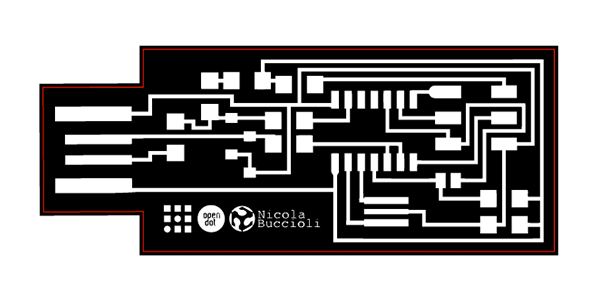
Redesign For the redesign I choose this board, which has a resonator instead of the crystal. In the pictures below there is the initial drawing (left) and the re-design made by Nicola Buccioli with a usb-adapter.
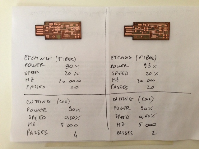
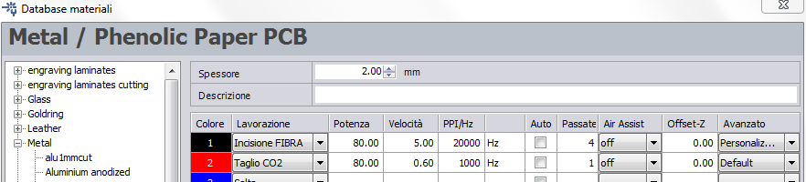
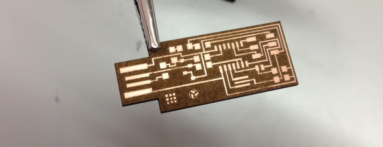
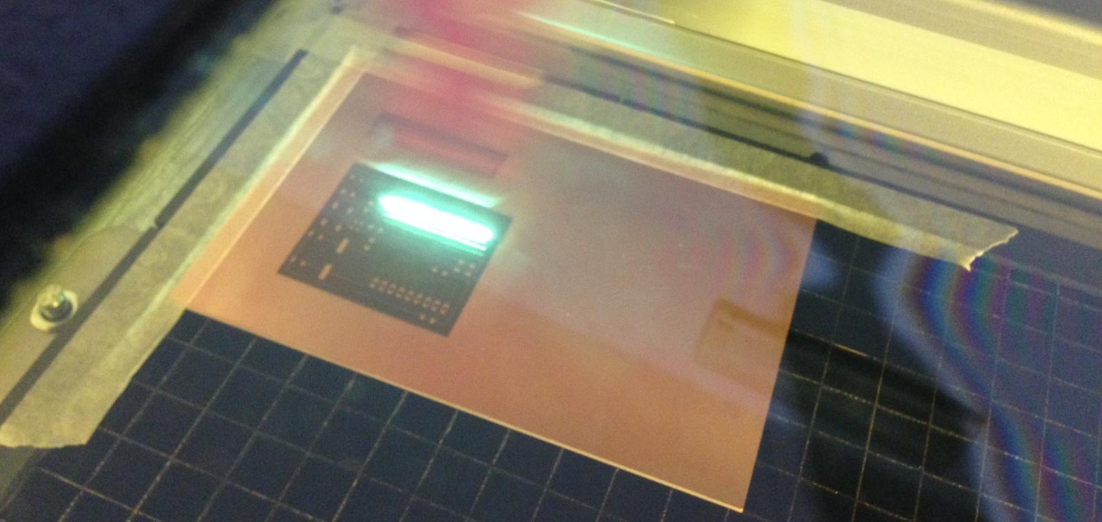 I used two boards as testing pieces, one is the Satshaskit and the other one is the FabISP version of Nicola Buccioli. Engraving happens with the use of the fiber laser pointer. The cutting, instead, is made with the regular Co2 laser. It is important to remeber to first engrave the cutting lines in order to remove the copper film. Otherwise the Co2 laser is not going to cut it. Below I report the results from the first two pairs of tests. On the left I only tried to engrave, while on the right I cut the FabISP.
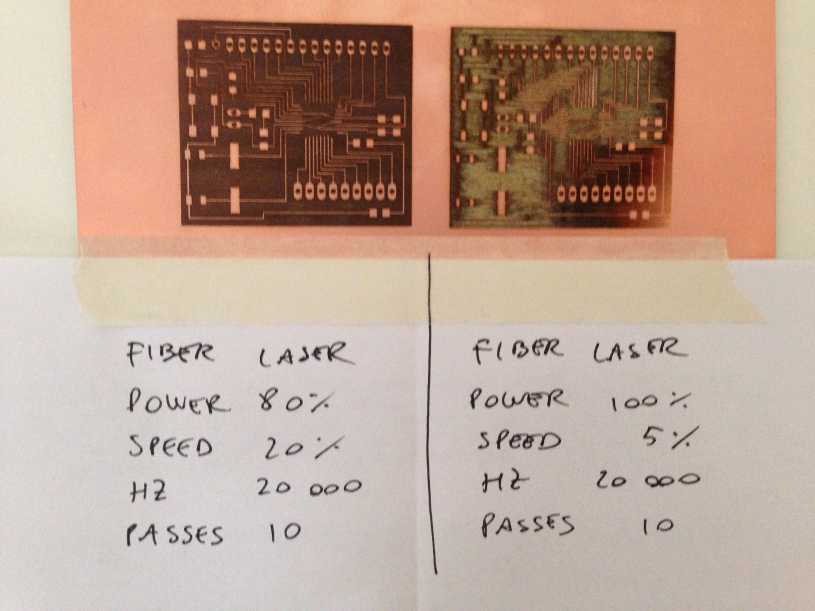
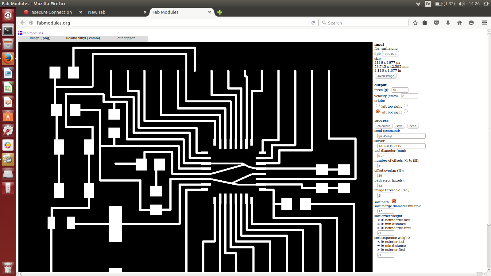
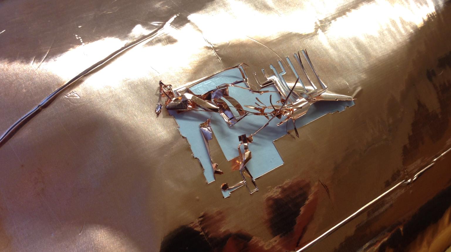
 At last, I decided to also try with the Roland vinyl cutter. We had copper film laying around and we gave it a go. Unfortunately, the traces were too tiny and the blade just started to drag them around at some point.
| Amount | Component | Schematic | RS-code |
|---|---|---|---|
| 1 | Resonator 20 MHz | RES | 811-7878 |
| 1 | ATTiny 44 | IC1 | 696-251 |
| 1 | 1K Ohm | R1 | 223-2265 |
| 1 | 499 Ohm | R2 | 679-2171 |
| 1 | 100 Ohm | R3, R4 | 223-2120 |
| 1 | 10K Ohm | R5 | 223-2394 |
| 1 | 0 Ohm | R6 | 679-1768 |
| 2 | Zener 3.3V | D1, D2 | 687-8250 |
| 1 | 1 microF | C1 | 766-1062 |
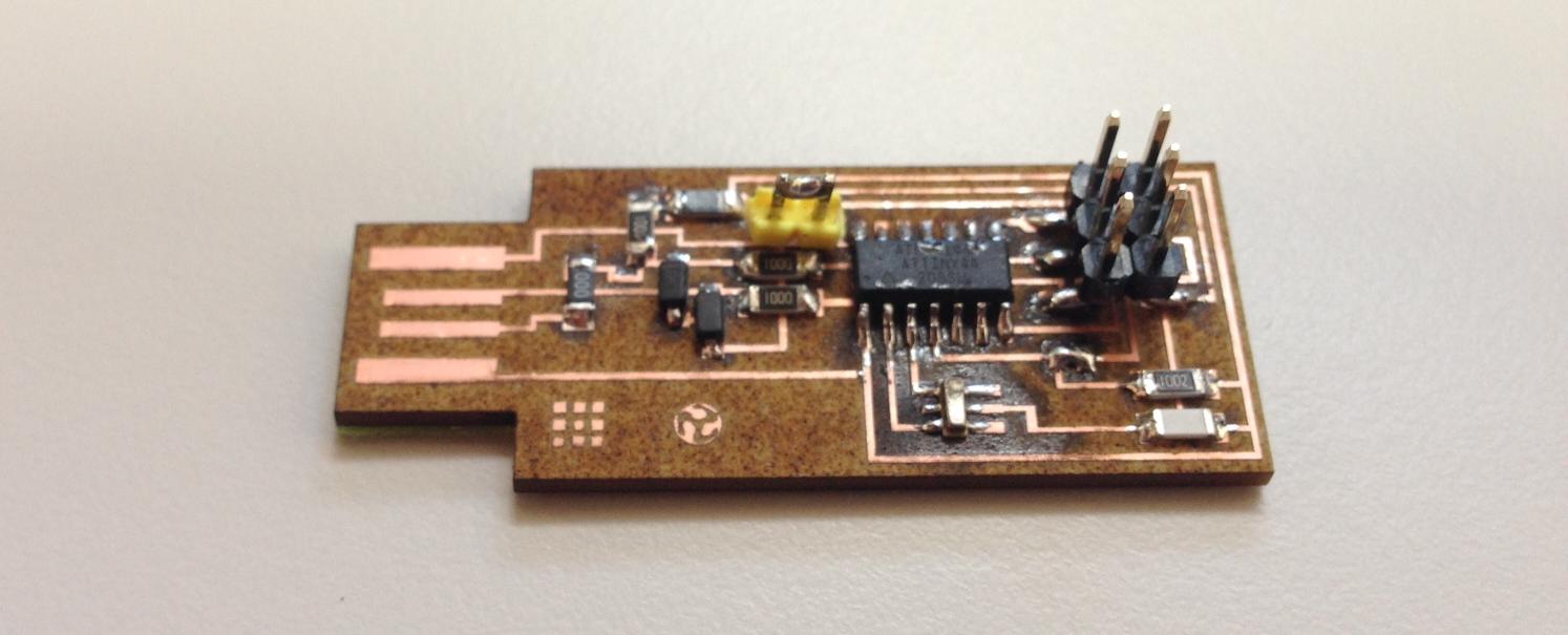 I then used Matteo's FabISP to program mine.
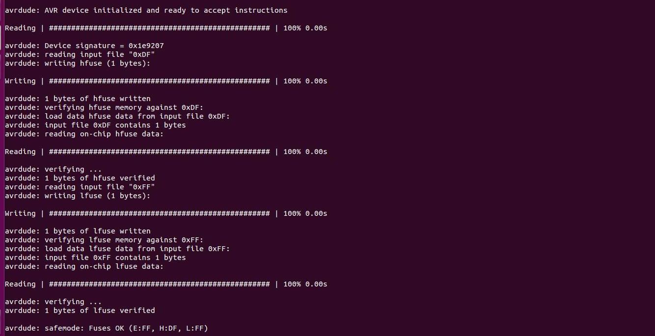
 This time both the make fuse and the make flash went well!
 Finally, I still had 2 more problems:
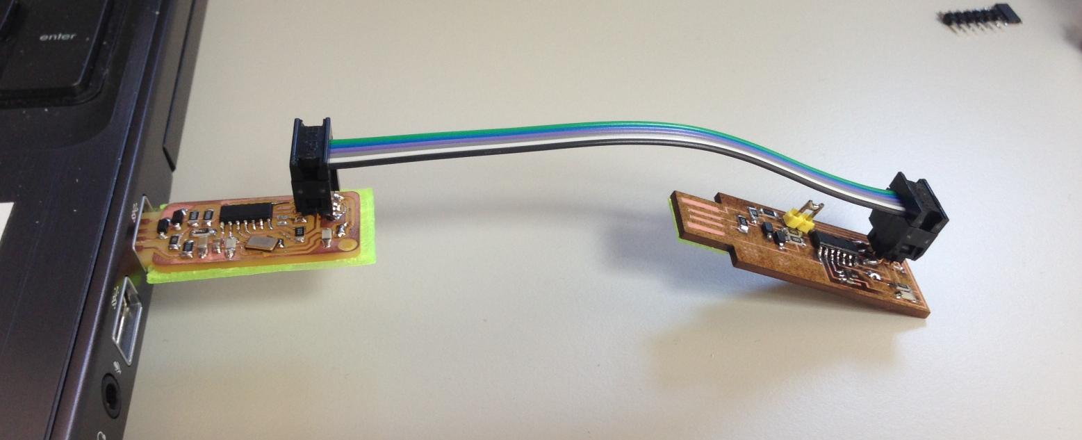
1.I had troubles in seeing my ISP from time to time, when launching the command lsusb from the terminal. I solved this by buying a male-to-female usb adapter that did the job.
2.The ISP could not power another board, because I removed both the jumpers. After I had checked the schematic, I resoldered the proper jumper.
Now the fabISP is up and running!
Finally, I still had 2 more problems:
1.I had troubles in seeing my ISP from time to time, when launching the command lsusb from the terminal. I solved this by buying a male-to-female usb adapter that did the job.
2.The ISP could not power another board, because I removed both the jumpers. After I had checked the schematic, I resoldered the proper jumper.
Now the fabISP is up and running!
Conclusions Thanks to the many mistakes I made I could learn a lot, especially how to solder fine components and look for bugs in a circuit. Apart from the many hours spent soldering, I also learned the basic of the process of getting a virgin microprocessor to work. I liked the topics and I completed the assignment only 2 weeks later the official deadline. On a side note, I did compare the use of lasercutting technology with the use of the Roland SRM-20 to produce. My feeling is that the lasercutter is a more appropriate way of fabricating PCBs. On the positive note: 1.You can easily produce 0.1mm traces withouth the risk of breaking them; 2.The whole file gets executed in one go, without having to manually replace hardware; 3.You can put fancy logos to your board! On a negative note: 1.It takes something like 15% more than milling;
Table of Content
Resources
- [1] Etching file
- [2] Cutting file
- [3] Case design
- [4] Firmware
- [5] Lasercut file