Exercise 04 Electronics Fabrications...
Intro
This week, we are going to execute electronics fabrications, in the tune of fabricating FabISP, an in system programmer that is made with ATTiny44 to program the AT family of MCUs.
Few years ago while I was looking for a small cap low cost MCU to replace the Arduino (ATMega328), I have chanced upon MIT High Tech Low Tech, the notion of using Arduino Uno (ATMega328) as the ISP programmer to program ATTiny84/85 has got me hooked URL here http://highlowtech.org/?p=1706
Since the discovery, I have designed and fabricated my own PCB Arduino ISP to program ATTiny85
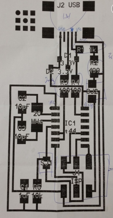
Coming back to this week assignment, I am going to explore 2 different type of Electronics Fabrications Machine that is made available to FabLab@SP, with two variants of FabISP the hello44 Fab ISP , and the very cool FabISP Key . The digital data resources to fabricate the PCB are downloaded from these URL.
OptionA: using FabModules to import a PNG file of FabISP Key to generate gcode that is generic across different PCB milling machine (we have one made in china al-cheapo PCB milling machine).
optionB: Using Eagle CAD to import a BMP file (256 colours, converted from a PNG) to generate gerber files meant for commercial PCB fabrication house or the LPKF103
in retrospective
It took me quite an effort and with the help of local guru to get my FabISP PCB board milled, stuffed, soldered, programmed, and fixed.
FabModules
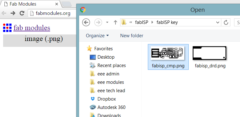
First, use a browser of choice to go to fabmodules.org. Select the PNG file of FabISP key
The following screenshot describe the imported file.
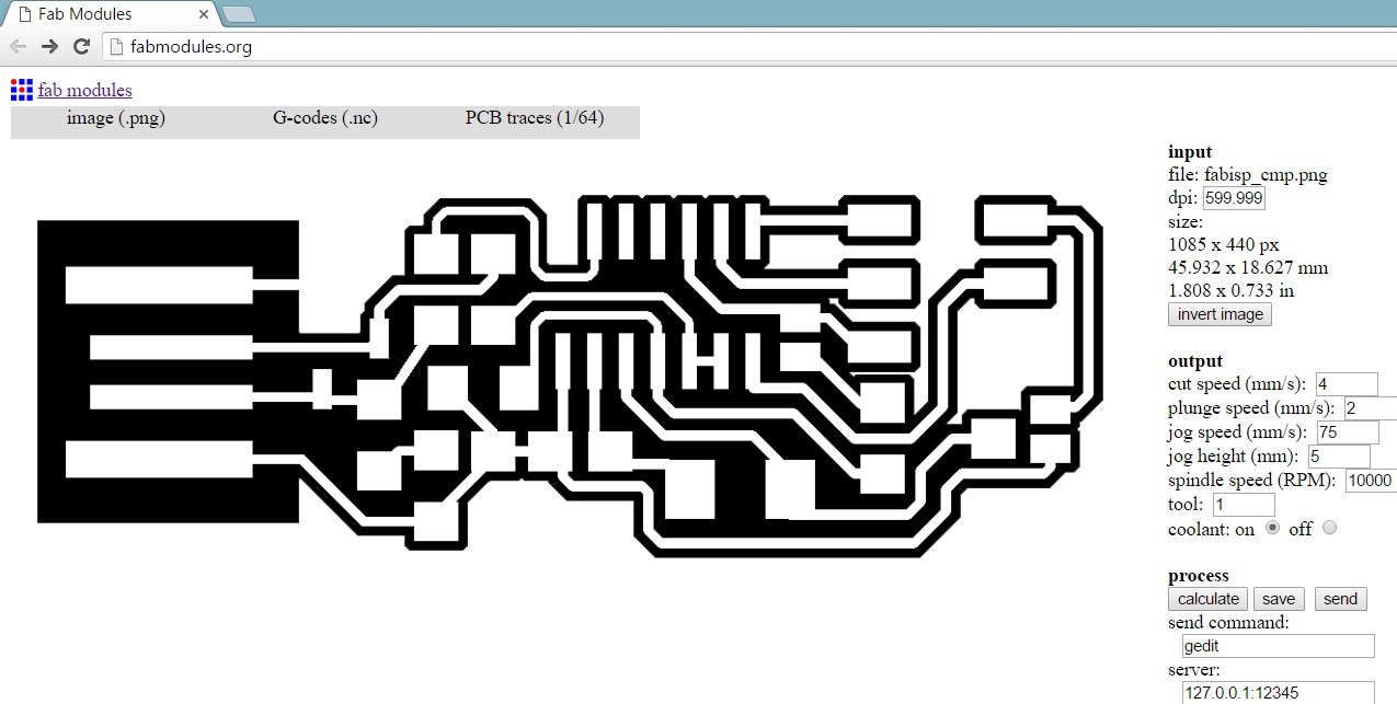
Then select the output format. FabModules support a myriad of output format. We are going to use a very generic file format the *.NC and the PCB traces to be 1/64” which is approximately 15mills. There are other parameters specific to the PCB milling machine used, and this can be set in this particular output tab. Then we are ready to press the calculation button to generate the tool path. The following screenshot depicts the process describe.
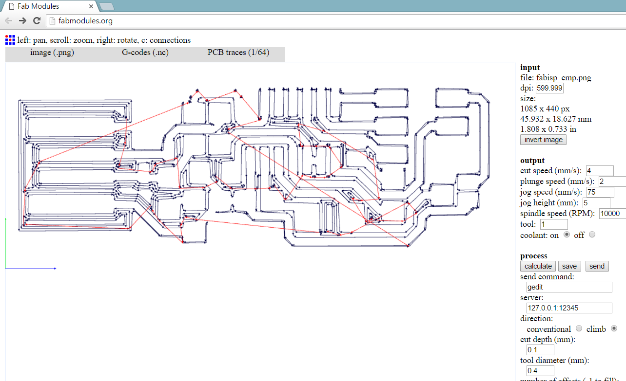
The tool path is generated, the following screenshot describe this step. As mentioned earlier, there are several parameters that are specific to the PCB milling machine used can be customized in this output tab. Cut depth, tool size, and such.
Once satisfy with the tool path, press on the save button to download the *.nc file. These steps are repeated for the board outline.
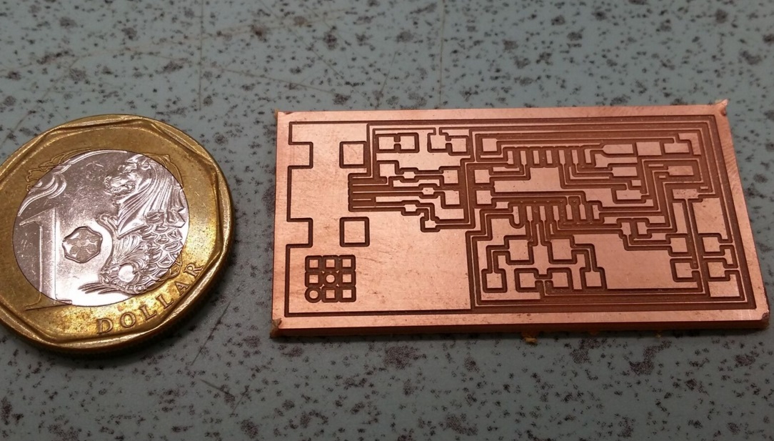
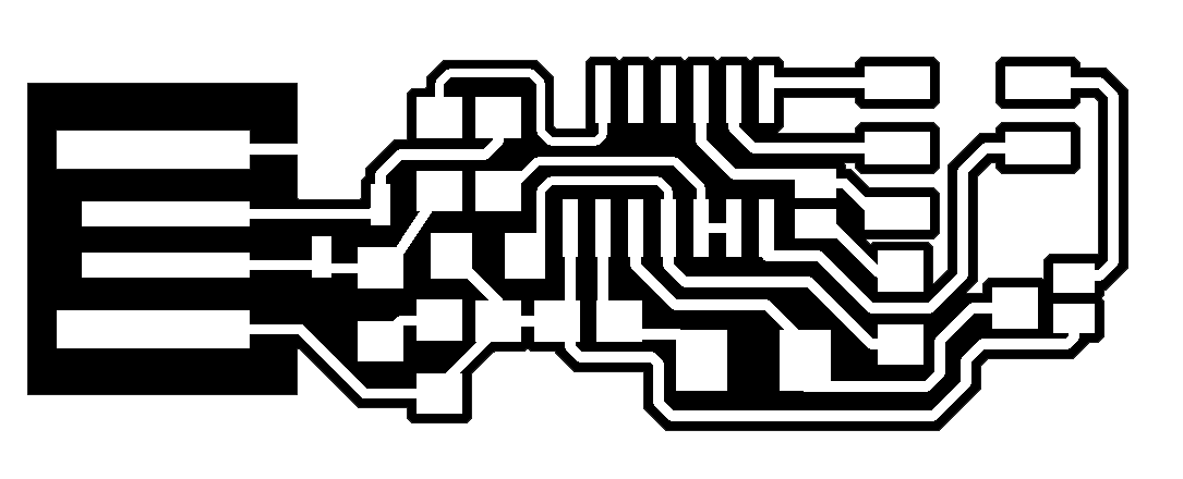
The FabISP key *.nc files generated From traces PNG and outline PNG with the use of FabModules can be downloaded here and here.
update: china made PCB mill PCB 2020B
The following milling parameters were used for PCB milling with the china made PCB mill.
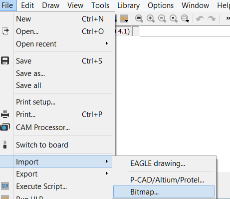
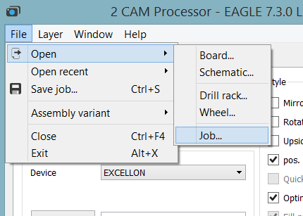
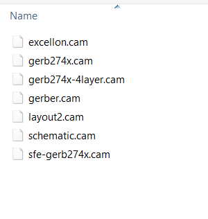
Eagle CAD
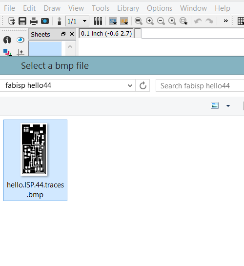
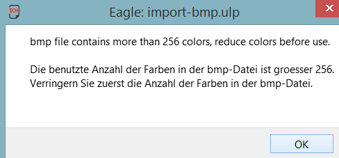
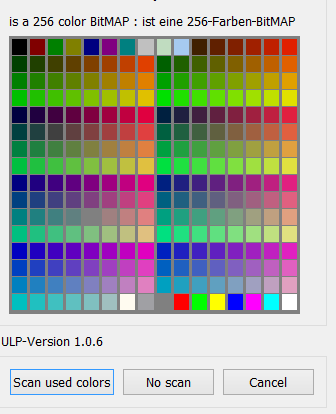
EagleCAD is one of the most recognized PCB design tool. Alternatively, Fritzing can be used to design PCB. EagleCAD has a very nifty utility, is the ability to import PCB design that is in the form of 256 colour BMP. The following screenshots described the import utility, the bmp file imported, and the 256 colours bmp file required.
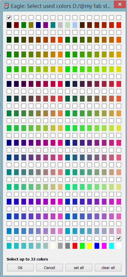
One the 256 colour bitmap files are imported, the next step is to decide on the colour scheme. In the PNG file, only black and white is used. In the following screenshot, we choose no scan.
We then proceed to select only the black and the white colour as per the next screenshot.
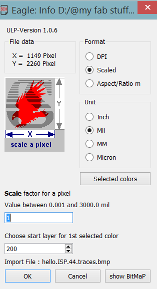
Next, choose the scale factor as per the screenshot below.
Once imported, the colour scheme of the PCB traces can be seen here
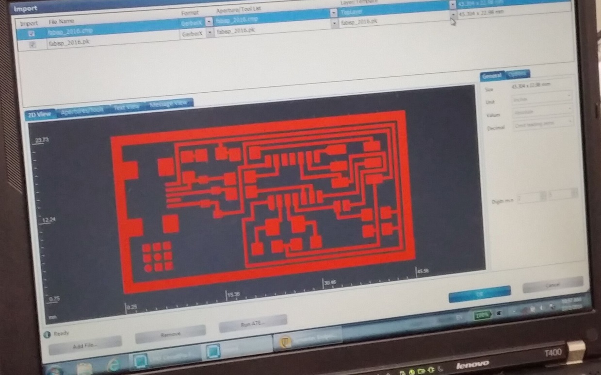
Next is to process the imported PCB traces into machine code, gerber to be precise. The following screenshots describe the process.
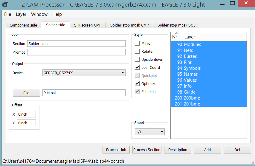
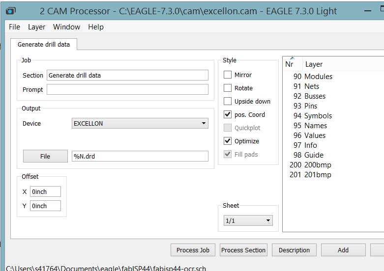
Repeat these steps for the outline file. The following screenshot depict the machine code generated with Gerb274x.cam and Excellon.cam (*.cmp , *.gpi, *.plc, *.sol, *.stc, *.sts , *.drd & *.dri)
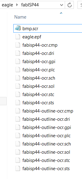
The gerber files for FabISP hello44 archived in a zip file can be downloaded here or here
LPKF103
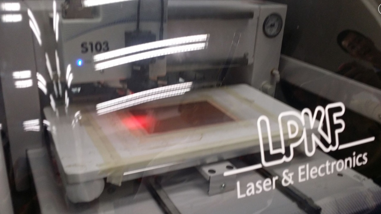
Once the gerber file is available. it can be used with any commercial PCB manufacturers. In FabLab@SP, we do have a PCB milling machine, the LPKF103 that takes in the gerber file as per describe in the following screenshot.
A standard operating procedure is available to operate the LPKF103. The following screenshot describes the start of PCB milling.
The following milling parameters were used for PCB milling with the LPKF103 PCB mill.
If you are interested to see the step by step setup of LPKF103 PCB milling use this URL to my Facebook album
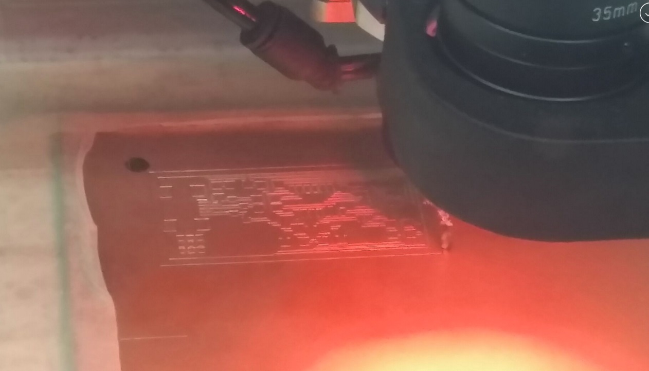
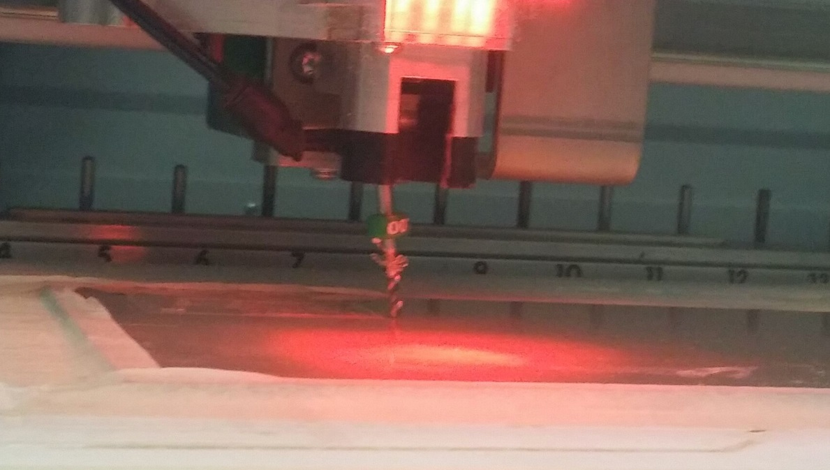
the following is the PCB milling in process.
milled PCB and problems faced
The following picture describes the 0.2mm universal cutter milling bit drop out during the pcb milling process. the error received was "voltage drop at cam". This machine is highly proprietary, we have to contact the vendor to service.
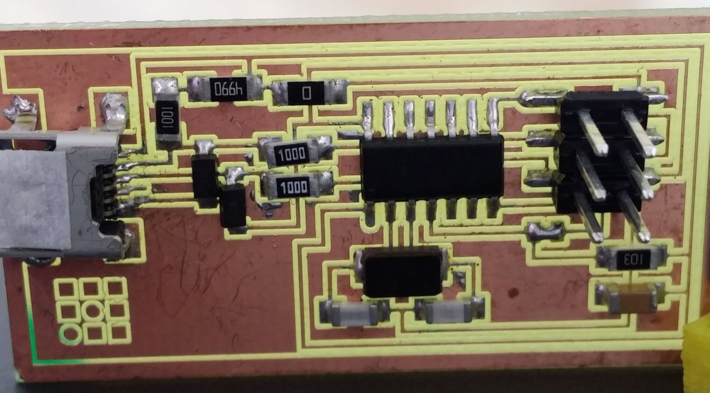
another issue faced with this particular pcb milling machine is the uneven milling. Some part of the FabISP-hello-44 milled correctly, but some parts are barely a scratch. of the many boards milled. The lower PCB milled is usable. but the traces are suprisingly finer that expected. This leads to some issues at the stuffing and soldering stage. Will elaborate in that particular section.
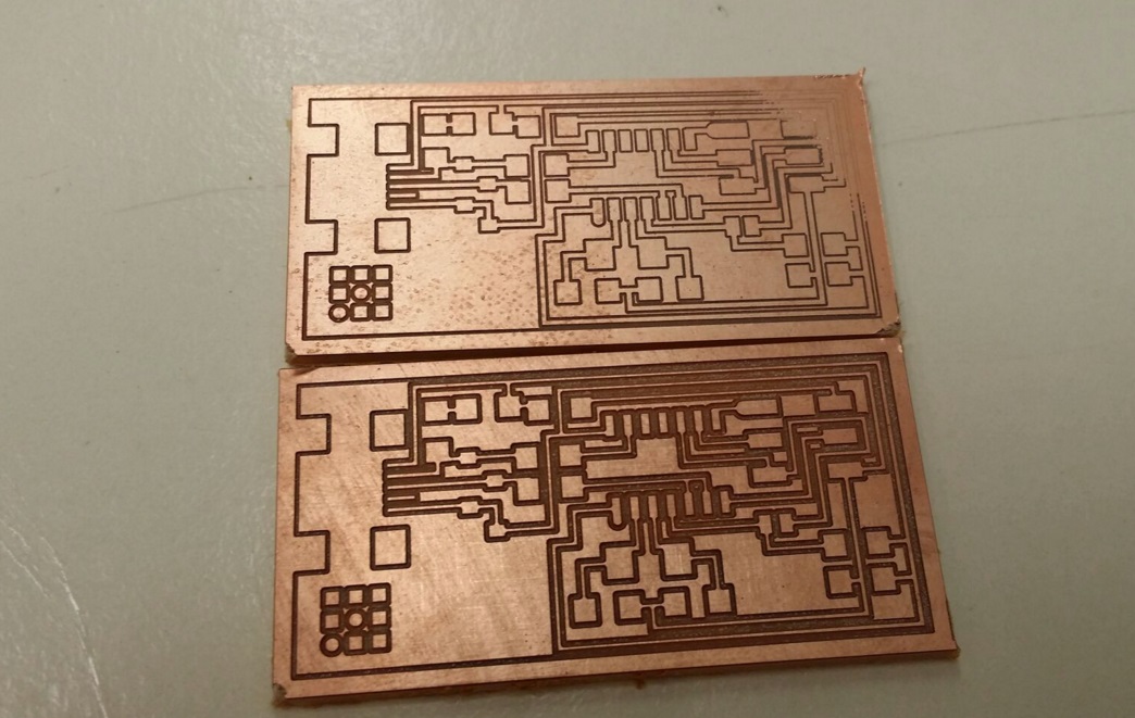
notice the traces that leads to the 20MhZ oscilator. The traces are suprisingly finer that necessary. Soldering on these traces lead to a bigger issue at a later stage.
The milled PCBs are subjected to a continuiity test. The traces are connected, even with the finer traces. Lesson learned: do not attempt to solder on milled PCB traces that are too fine. The copper traces might be "lost" due to the heat treatement.
Stuffing & Soldering
I have soldered successfully QFN packaged ICs with a dot pitch (spacing between pins) of 1.27 mm via the process of beta testing of ESP32 board, and the step by step guide available on instructables http://www.instructables.com/id/Beginners-ESP32-Guide-to-Assembly-Testing/
PCB milled board requires TLC (Tender Loving Care). First we need to inspect the cut path, whether the cut is deep enough to isolate the traces. If not, TLC with a fine tip blade is needed to score the traces. Oxidized copper is very difficult for the solder to stick on. Neil has suggested to wash the milled boards with soap and water to remove any gunk.
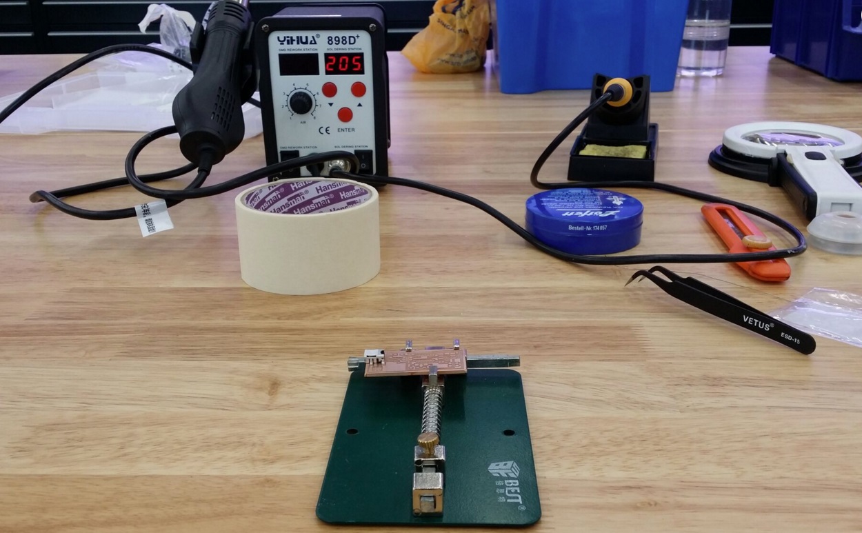
before soldering job begin, i personally prefer to have my soldering station setup as per the picture below. The tools necessary have to be within reach. Summing from my previous experience on soldering 1.27m dot pitch, the methododology of soldering SMD is to apply flux to the pads, tin the pads, and then attach the SMD components with tweazer, and dab with a fine tip solder iron heated at 205degC.
soldering & stuffing strategy
First things first, i really hated soldering the micro usb smd connectors. Given more time, i will fab the FabISP-USB-key variant, and 3D print a base for it to prod it up. upon the recommendation of Mr.Chew and Mr.Dorville, all students are to soldered the FabISP-hello-44.
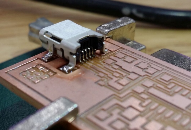
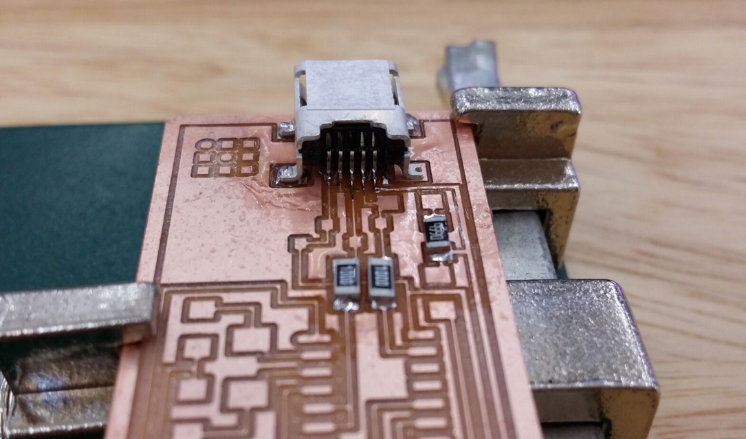
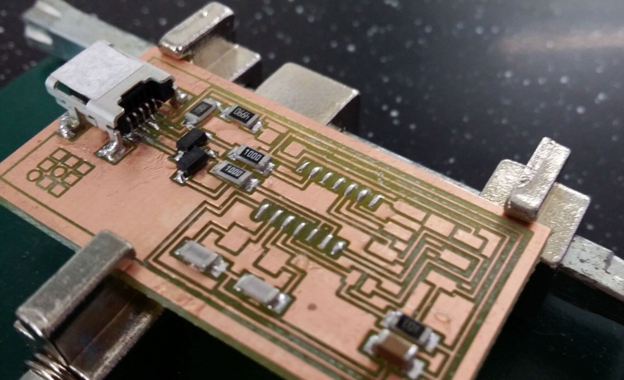
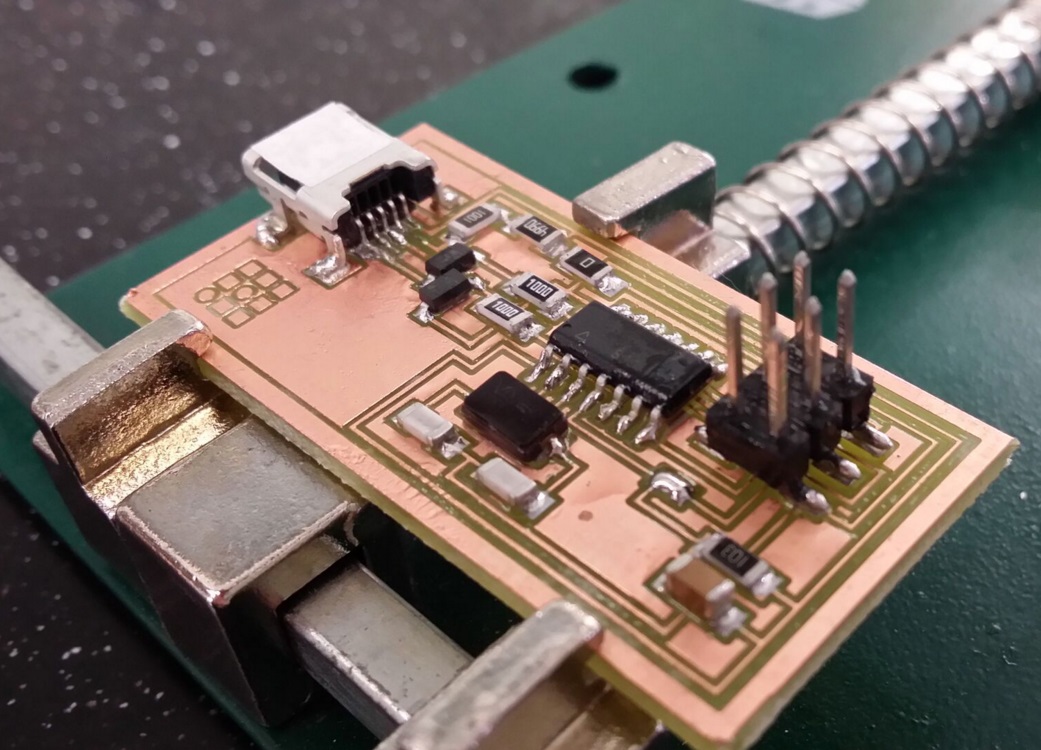
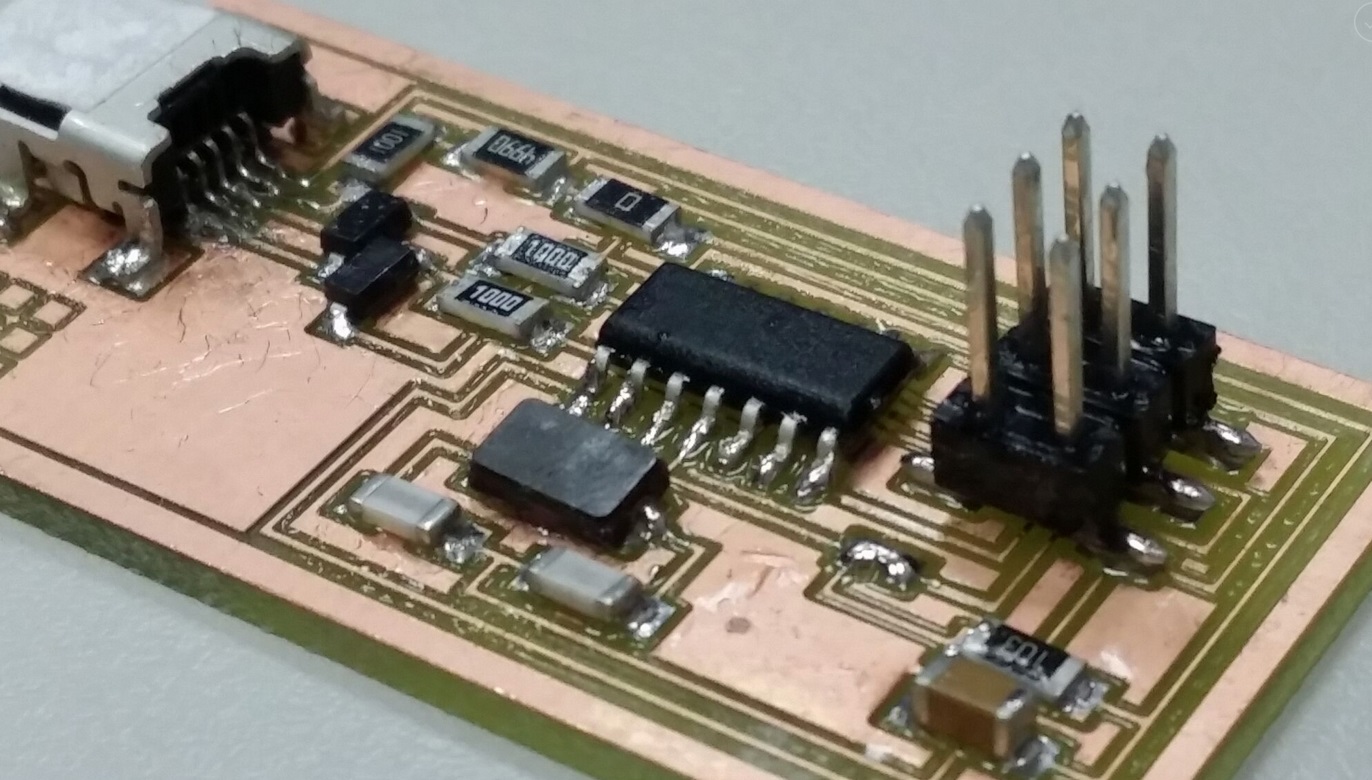
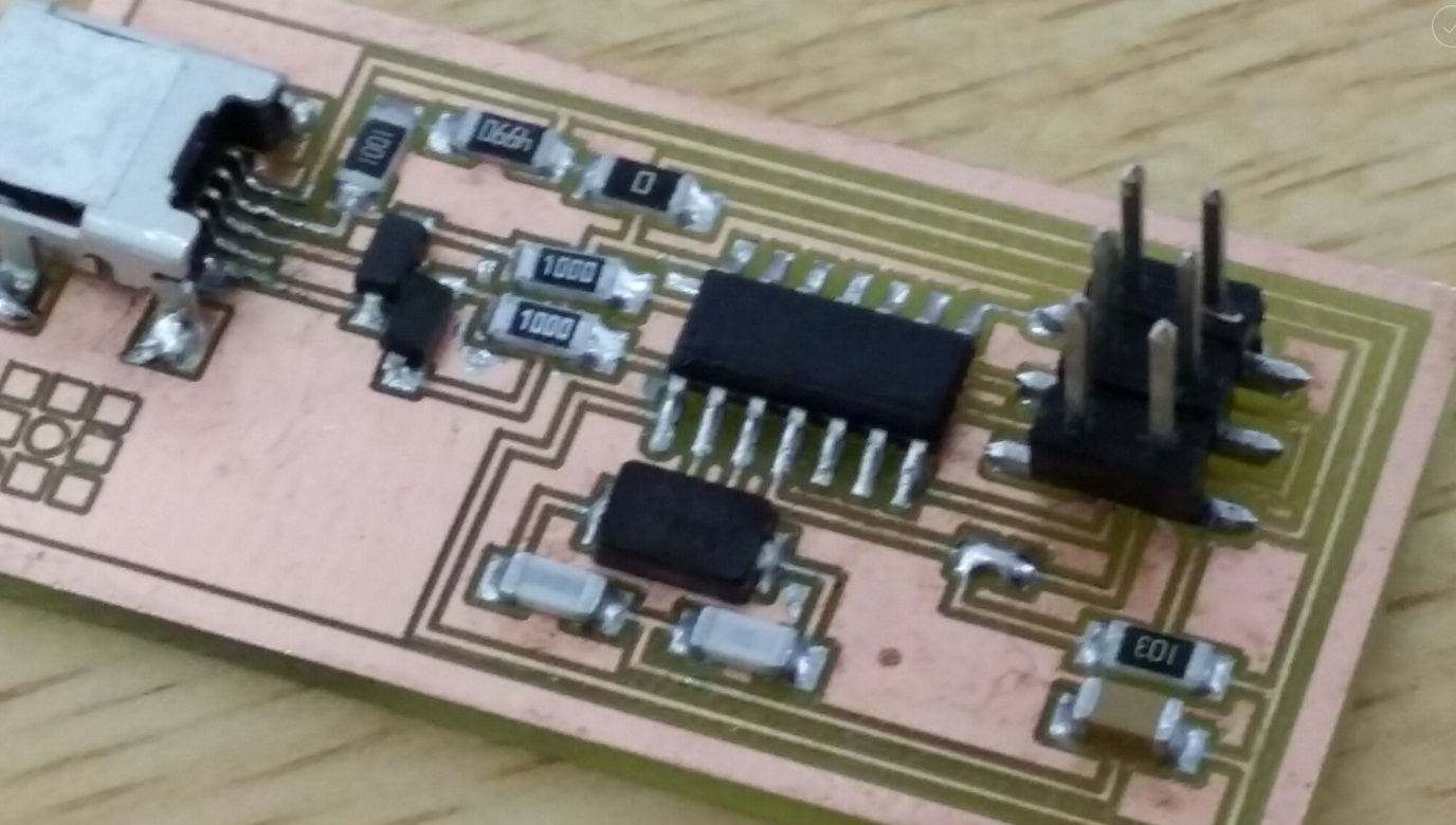
Refer to the picture below for the pcb trace. First, solder the microUSB connector, and peform continuity test after soldering it. If the micro usb pin outs are not correctly soldered, it is best to bin it, or attempt to repair with reflow hot gun. Next, move to solder 1206 packaged passive components that are non polarized. use the flux-tin-solder method mentioned earlier. components with no polarity is great to get into the zen mode of soldering the SMD components. Then solder the SMD components with polarity. Special precautions are taken to ensure the polarity of the SMD components. They are too small for the naked untrained eye. I have used magnifying glass to identify the cathode side of the zener diode (mark with a bar), and also the vcc pin (mark with a notch) on the attiny44. I leave the 20MhZ oscilator to the second last to be soldered, because it was blocking the way of my solder iron to solder the attiny44. Lastly, solder the 2x3 male pin header.
the following pictures describe the strategy mentioned above.
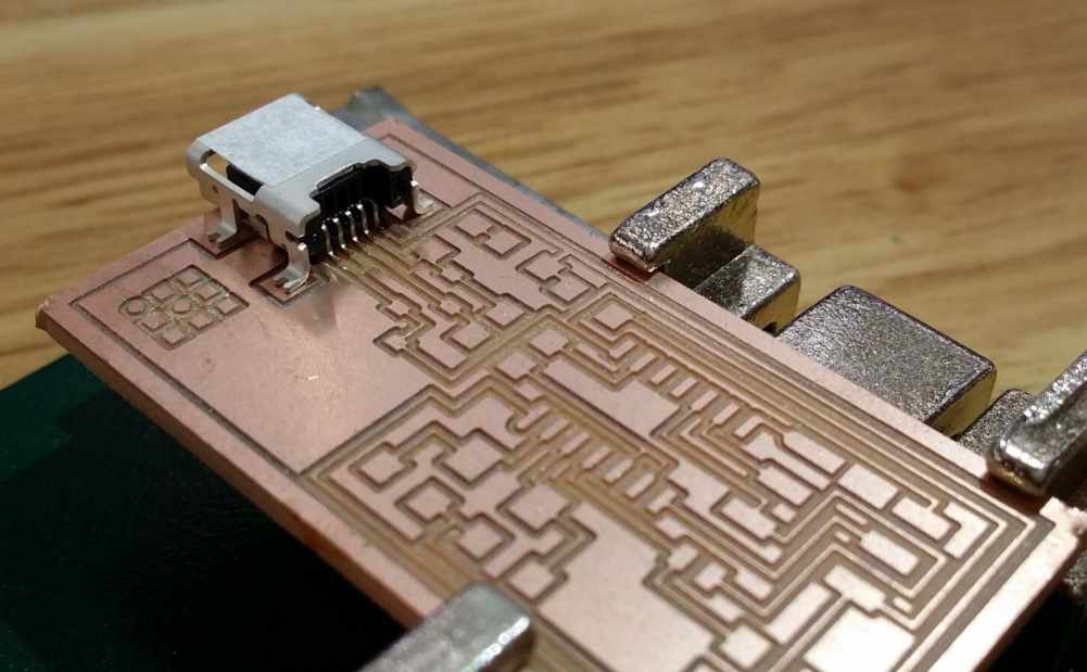
Place microusb connector. solder the holder of the microusb connector first, follow by the pins. test the soldering connection of the microusb connector with continuity test. Satisfied with the outcome, proceed to solder the passive SMD components.
not too shabby soldering.
tin the pads prior to soldering the components.
looks legit.
At any time if the pins are shorted when soldering, do not panick. take a deep breath, take a step back, realign your thoughts and then desolder it with the reflow hot air gun or solder wich to remove the excess solder.
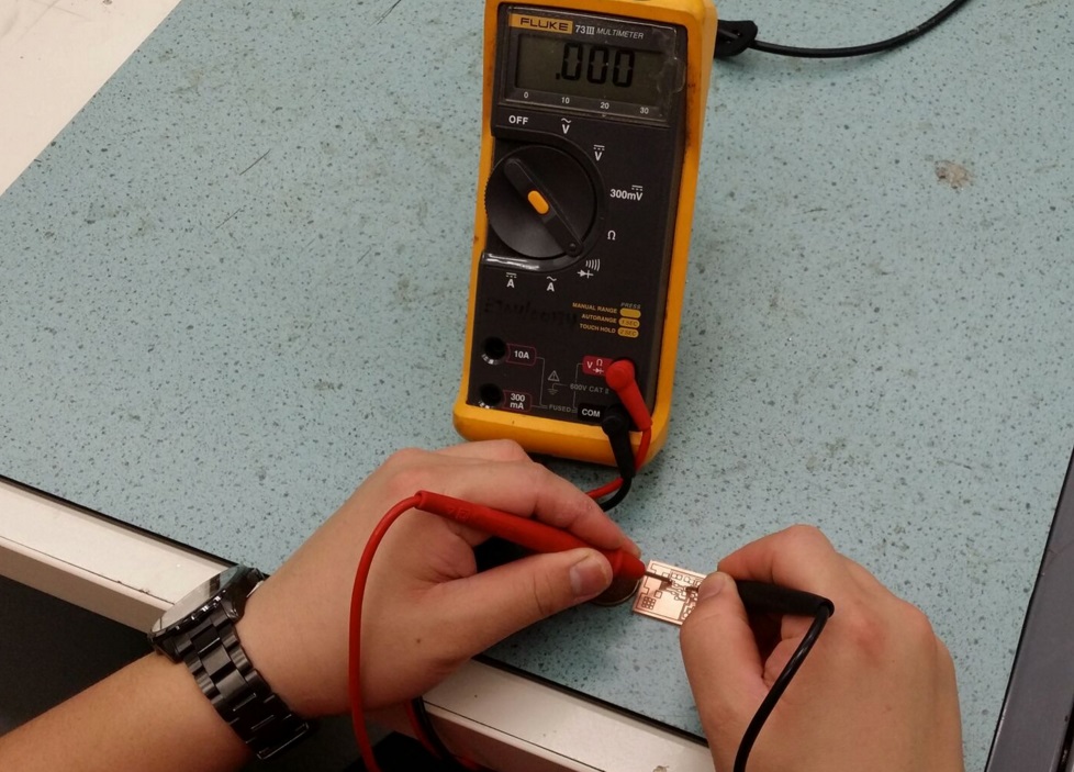
testing of the stuffed PCB
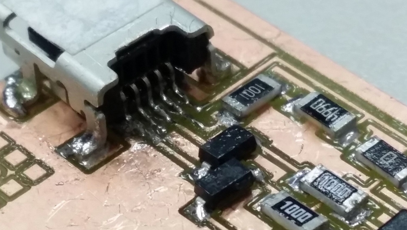
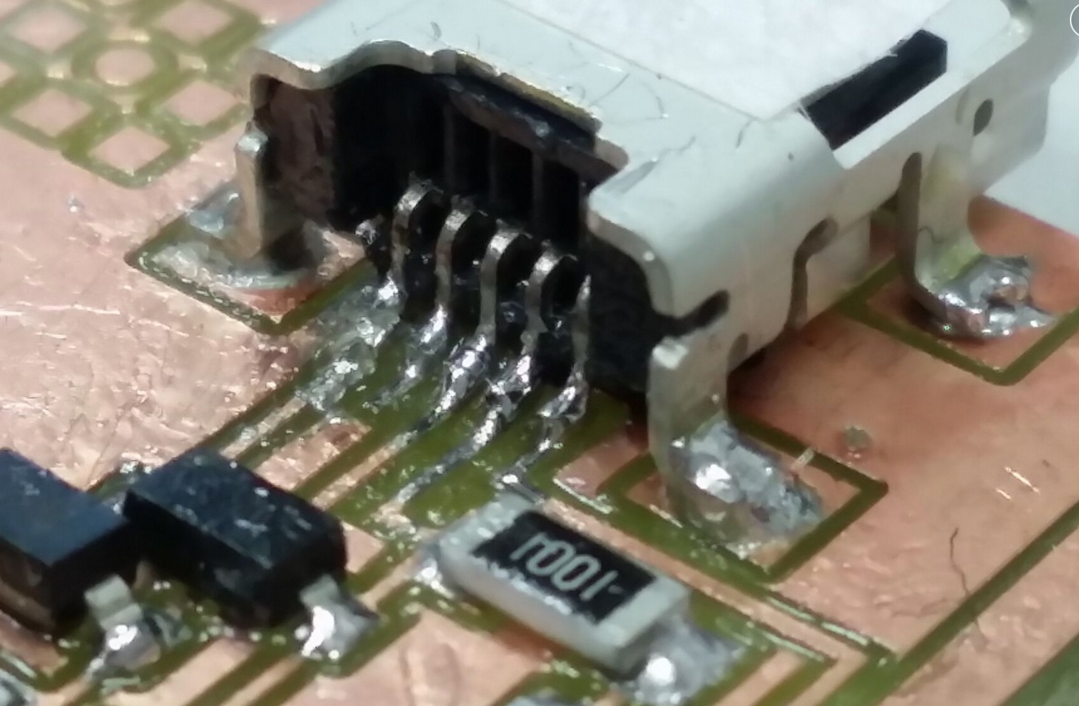
completing the soldering is only one third of the story. The stuffed board needs to be tested with continuity test. Eyeballing the soldered PCB simply will not do the job. One of the traces leading to the microusb was tested as negative. the trace is disconnected. but the funny thing is, right after soldering the microusb connector, continuity tests were carreid out on each pin on the microusb connector to the traces and these tests passed! no, i am not drinking on the job.
The problematic pin was given some TLC; picture on the L is before and on the R is after.
 |
 |
this board is now ready for the smoke test.
traces that are too fine
The following picture desribes the problem faced when soldering a milled PCB with traces that are too fine or over milled. I was overconfident that i was able to meet the cut with my soldering skills on a less than perfect board. but reality is, it doesn't. The very fine traces simply "vanishes" after tinning and failed the continuity test.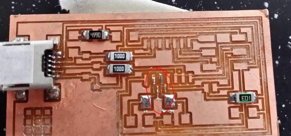
This PCB board has to be chucked.
smoke test
now we connect the Fab-ISP to be programmed to be an ISP. There are 3 ways to program FabISP as the ISP, use a commercial programer, use another FabISP, or use an Arduino. Since i do not any another FabISP with me at the time of writing, i only have an arduino, so I use it as the ISP to program my FabISP as a ISP.update: Arduino as ISP
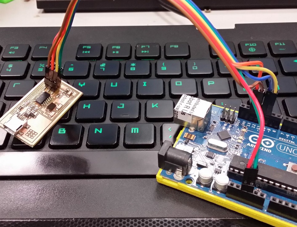
The following wiring scheme is used, following the comments in the code Arduino as ISP.Reset pin on FabISP is connected to pin10 of Arduino Uno.
MOSI pin on FabISP is connected to pin11 of Arduino Uno.
MISO pin on FabISP is connected to pin12 of Arduino Uno.
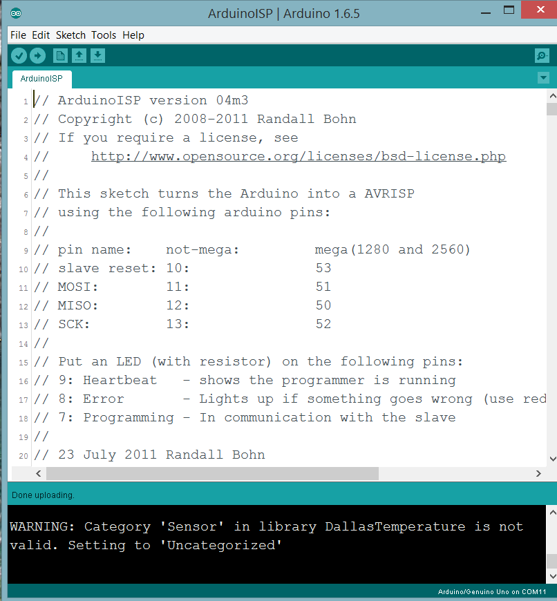
SCK pin on FabISP is connected to pin13 of Arduino Uno. In arduino IDE, there is an example code on Arduino as ISP as per the following screenshot.
The wiring from the arduino pin to the corresponding 2x3 pin headers on the FabISP
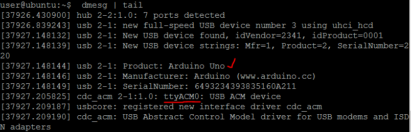
There is a quick tutorial offered by FabAcademy on arduinoISP The arduino need to be programmed with Arduino as ISP before connecting to the FabISP. locate the port arduino is connected
follow the step by step guide on programming the FabISP procedure to program FabISP
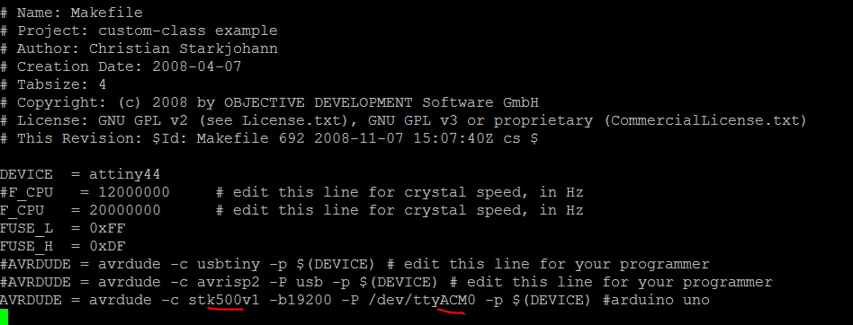
The modified makefile to program FabISP with Arduino as ISP be downloaded here
Locate the make file, and make the following edit to use of arduinoISP to program FabISP.
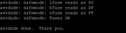
the following screenshot depicts the successfully program FabISP.
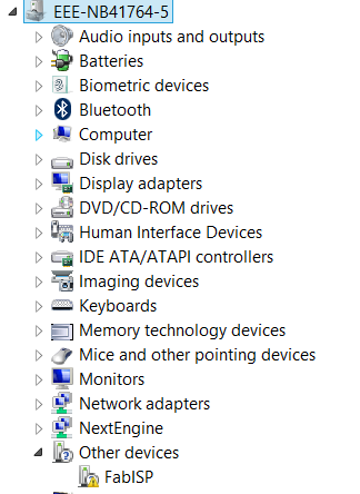
Plug to a windows8.1 machine, the FabISP should appear in device manager.
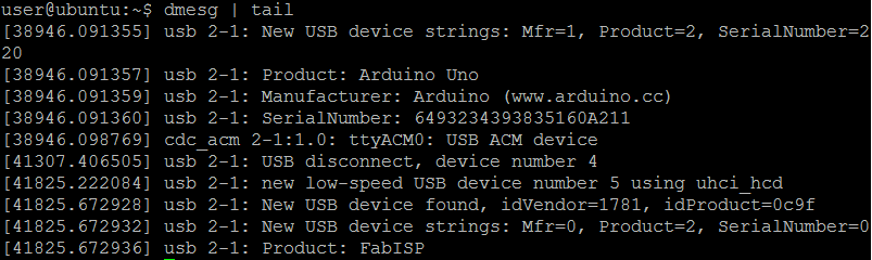
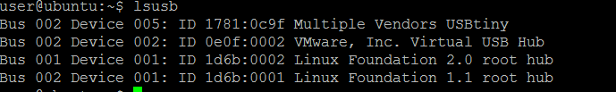
plug to a unbuntu machine, the FabISP should appear as a USBtiny device in linux
troubleshooting the stuffed and soldered FabISP PCB
After programming successfully the FabISP, for some reasons, it doesn't show up on the computer when plugged into. I have tried to use a MacBook pro, a Lenovo with win8.1, and a ubuntu, but to none avail. the following screenshot depicts the failure in win8.1. In mac or linux, it doesnt show up at all.
After all the line tracing, continuity test on the traces from the microUSB connector to the rest of the SMD components, eyeballing under the magnifying glass, but the same error still persist. Local Guru Mr.Dorville FabAcademy 2015 alumni showed me a neat trick to get the FabISP board to function and detectable by the computer. Mr.Dorville's final trick is to do a reflow (also known as reballing) of the solder joints with the use of the hot air gun. The soldered FabISP PCB is tiltled at an angel such that when treated with hot air from the hot air gun, the gravity will pull the solder to cover any possible dry joints that are undected by the human eye or multimeter. My FabISP PCB was detected by the computers after some reflow TLC! The following pictures depict the solder joints after the TLC with hot air gun.
 |
|
troubleshooting the ubuntu x arduinoISP
if any chance ran into this problem "avrdude: ser_open(): can't open device "/dev/ttyACM0": Permission denied" need to assign rights to the user to use the serial device with these commandssudo usermod -a -G dialout my_user_name
sudo chmod a+rw /dev/ttyACM0
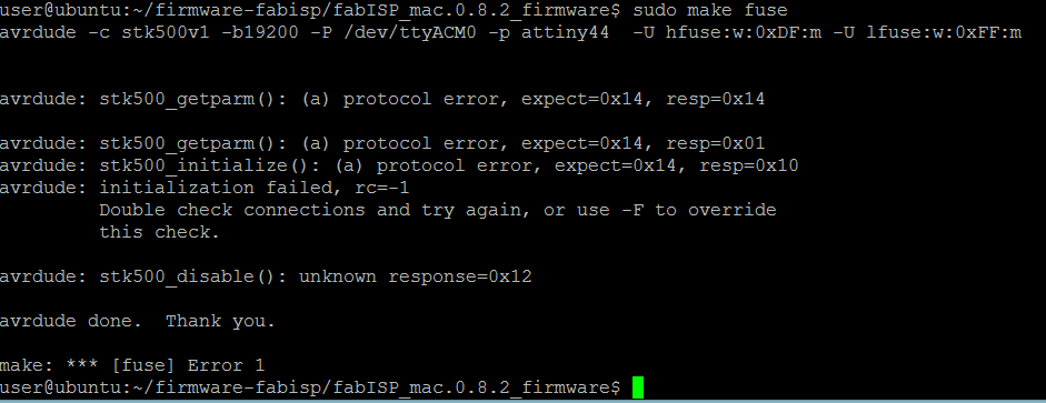
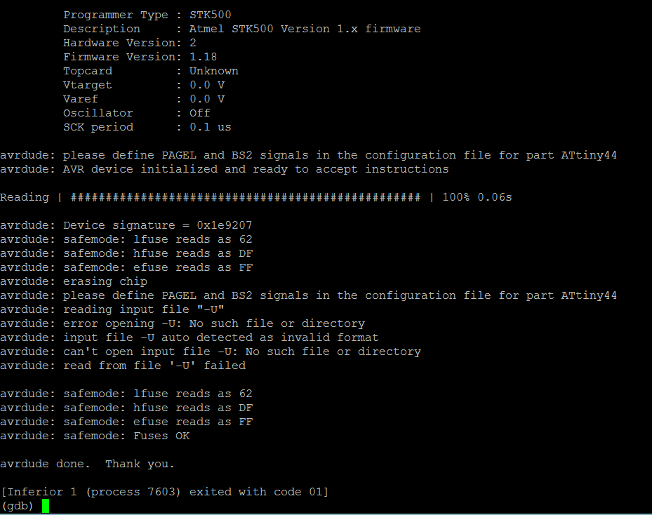
if ran to the error above "avrdude: stk500_disable(): unknown response=0x12" the blog post here depicts the use of gdb to pause, just to solve the error. the FabISP executed the "make program" and the following is the output
Source files Download
The FabISP key *.nc files generated From traces PNG and outline PNG with the use of FabModules can be downloaded here and here.
The gerber files for FabISP hello44 archived in a zip file can be downloaded here or here
The modified makefile to program FabISP with Arduino as ISP be downloaded here
Reference
SMD size chart: http://www.topline.tv/SizeChart.html
The new FabModule: mods.cba.mit.edu
The FabModule: http://fabmodules.org/
fabisp key http://fab.cba.mit.edu/content/projects/fabispkey/index.html
fabisp hello44 http://fabacademy.org/archives/2015/doc/electronics_production_FabISP.html