week 03 | 2016/02/17 - 2016/02/24 | electronics production
16
Stage 2: PCB production, milling
17
My second stage of this assignment was milling my PCB on our LPKF S63. This is a specialized PCB mill which comes with special software and tools. Due to the fact that this is my first time using this PCB mill, Christoph gave me an instruction on this machine. Sorry for the german GUI on my pictures!
18
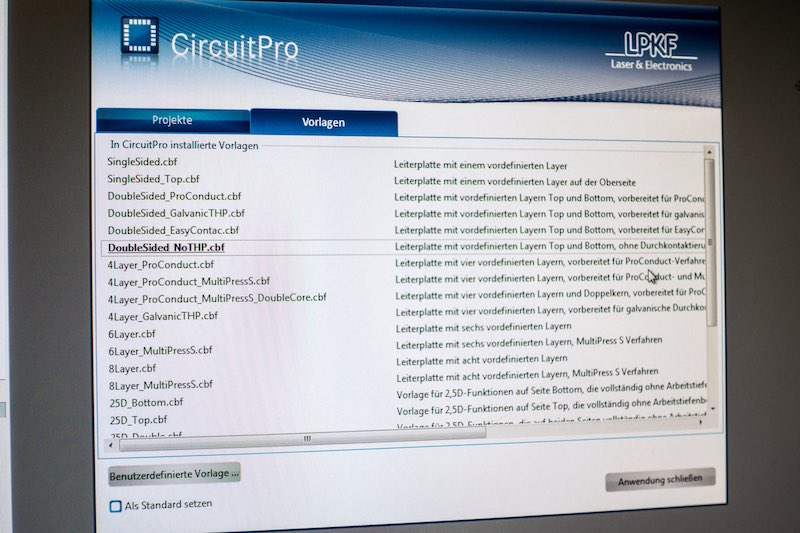
First, I had to choose the right preset, which is double-sided without through-hole plating in this case.
19
20
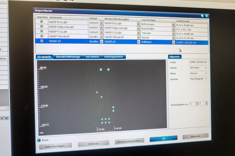
The second step was to import my Gerber files from KiCad into the LPKF CircuitPro program. In this step, I had to assign all my layers to the program internal layer structure. There is also the option to name the layer direct the right way in your PCB design program, which saves this step.
21
22
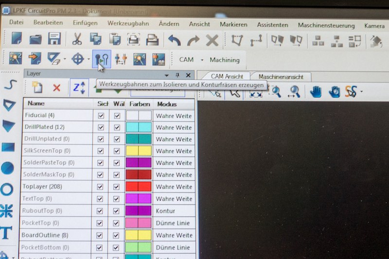
The third step is to generate the milling paths, just click on this button.
23
24
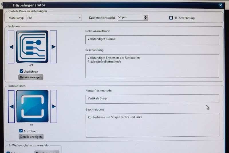
The milling path generator gave me the option to select the rubout method. I chose a full rubout. In the second option I decided to use vertical fins, which fit best to my PCB design. There are already the options for horizontal, vertical and horizontal and edge fins, depending on the PCB design.
25
26
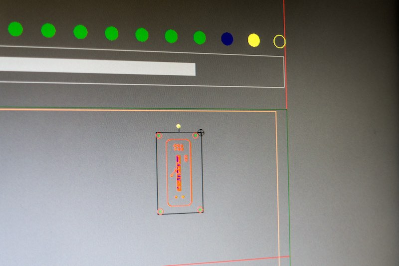
In the forth step, I had to chose the position where the PCB mill should mill my PCB. To position the PCB, make a click on mousepositioning, click on the wanted place of your machine bed, de-select the mousepositioning button and just drag and drop your PCB to the origin you set before.
27
28
Some minutes later, the machine asks you to turn the PCB after milling the bottom layer. After turning your PCB, the machine asks you to check if it has detected the right origin through the setted fiducials in the pcb.
29
30
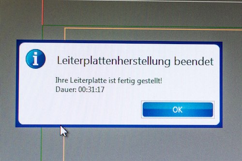
Finished!
31
32
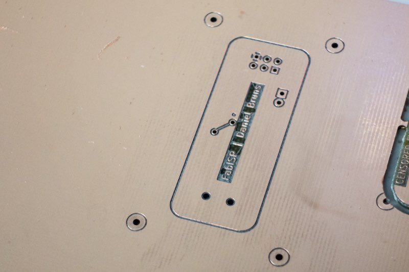
This is the top layer of my PCB before cleaning, directly after the milling process.
33
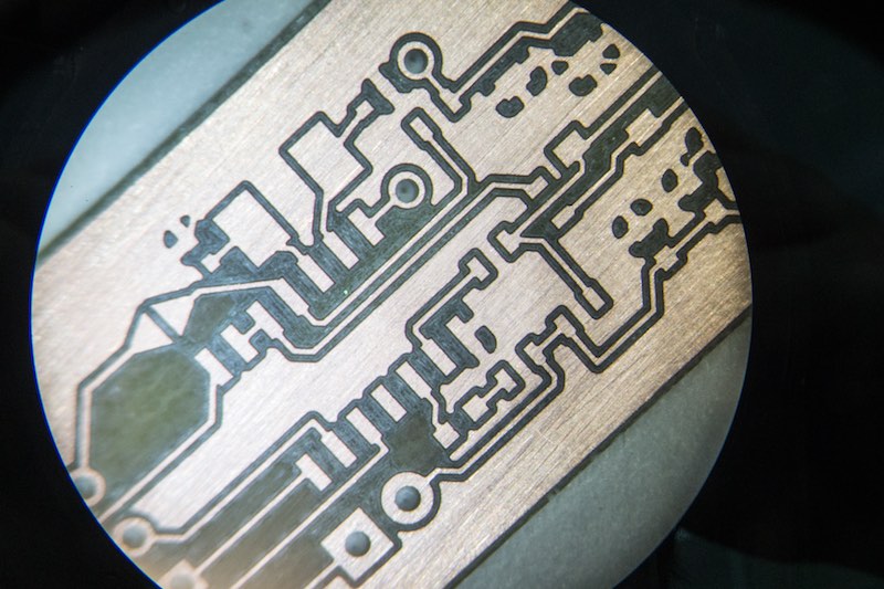
34
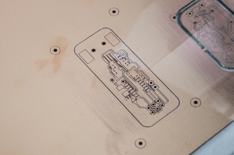
Under our microscope the PCB looks good, too. :)
35
Use this shortcut to stage 3! :)

This work by Daniel Bruns is licensed under a Creative Commons Attribution-NonCommercial-ShareAlike 4.0 International License.