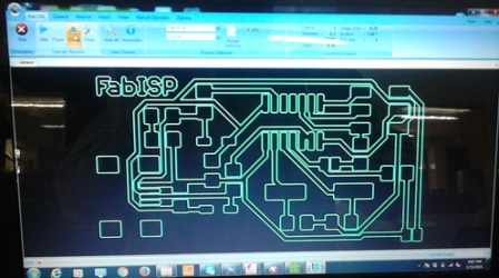
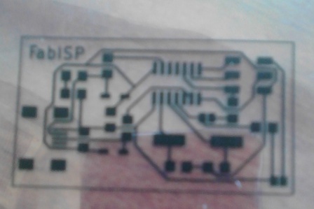
The files were downloaded from Fabisp here the files were in different formats of schematics and brd. Use Eagle to open them in ordr to create Gerber Files.
Read
The files were downloaded from Fabisp here the files were in different formats of schematics and brd. Use Eagle to open them in ordr to create Gerber Files.
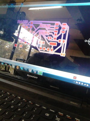
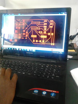
After the generation of the Gerber files, transfer the gerber files to IsoCAM which reads Gerber and drill files. It is also used for convertion of data and editing. The data to be drilled is saved as .ne
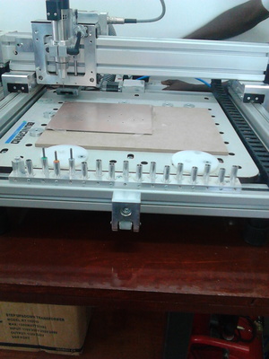
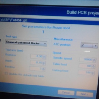
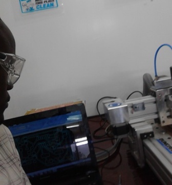
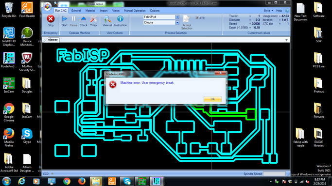
From here, we need to create a milling data and save it . it will automatically take the default extention. In our case we use the Computer Controlled Drilling and Milling Machine and the RoutePro 3000 to do the milling and drilling. I did all the settings and trying them fro the base, thickness under general; I the X and Y offsets leaving the scale at 10. The material settings were abit obvious leaving them at Length 160, Width 100 and Thichness of the copper at 1.36mm.
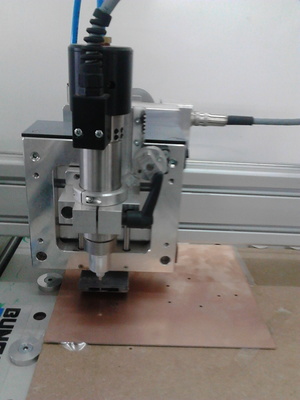
From here, I proceeded to the Machine where, I fixed the the workpiece on top of the base (sacrificial board). Unfortunately the cello tate I was using was not sticky enoufg and the pcb was not so flat on the board. This was evident as some lines could be milled dipper compared to other.Watch work in progress
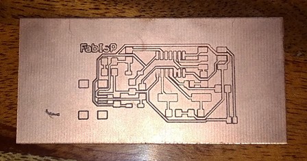
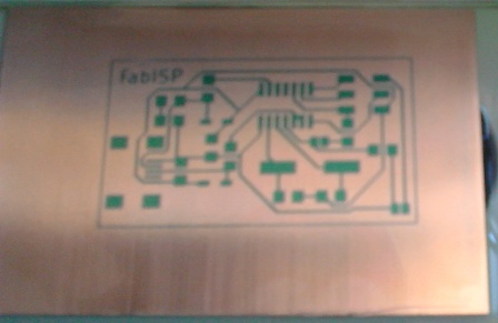
After the milling, I brushed off the dusts and here is my finished board
On the second trial I followed all the processed above well but when it comes to settings, I did not get it correctly and realised that it was milling much dipper aand so I stopped the work from the comp to work on the settings. I did not remember to replace the test tools in their correct positions and chuck before restarting . This error became very expensive when our Test tool broke in the process
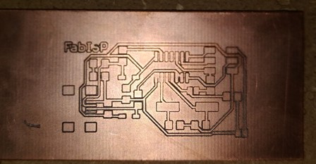
Anyhow, after correcting the error, I proceeded with my milling to the end and my results were amazing. Here is my completed FABISP board ready for stuffing
Other than Computer Controlled Milling of PCB, you can also use Screen Printing method, Vynil Cutting or Etching which is also known as the (Wet Process).
For my case, I chose to use the Etching Process eventhough it was against the spirit of Fab Academy. This followed the fact that the milling machine at Gearbox had mechanical problem which kept on breaking tools when in opearion. The challenge persisted even wtih alot interventions. The importation for other new tools also took fairly longer time and so I could not wait for them while the assignments were piling. The Fablab manager xxxxxxxxxxxxxxxxxxxxxxxxx
Below is the Etching Process
Other PCB Making methods worth trying includes Laser Cutting a PCB with a CO2 / Fiber Trotec laser cutter. Learn more from the Tutorial. We will look into 3D Printing if such can be used as well
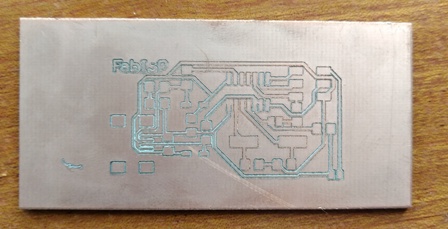
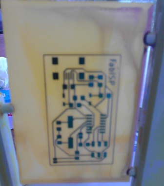
For some reasons, I changed from the previous design and decided to use the FABISP Key design (20MHz Crystal Version) which has the USB end. I downloaded this, Printed it on a clear paper and took the etching process since our milling machine was overloaded with work. I had earlier on practiced both milling and etching processes and was so comfortable in using either of them.
I cant fail to note that the chemical failed to remove all the copper layer well on some parts of the board in the developer and this would affect the connection. It prompted me to etch for a longer time. This however led to more damage to my board which then failed continuity test.
Now, I had to do another process of etching again for a fresh board. Luckily, this was well done exept the reverse side which also failed to etch well. I failed to know the reason for this but it ranged from weak developer chemical to previous defect on the board
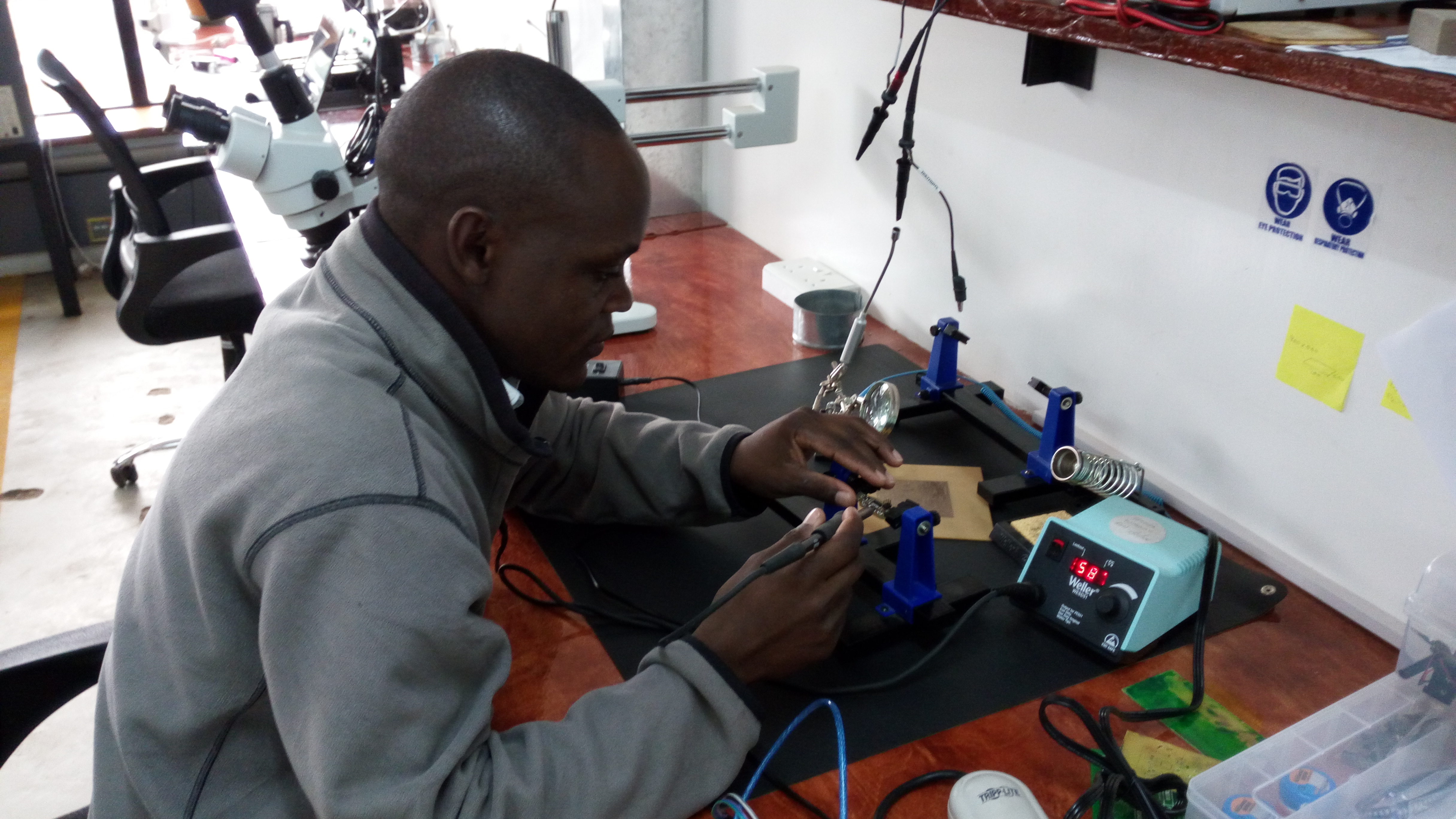
Now that may board was ready, I proceeded to solder the board. Bur=t first went through this tutorial on How to solder
In soldering, I first applied soldering paste on the board and then starting slodering by handling bigger components first and from the centre outwards. Soldering the Microcrontroller for the very first time wasnt easy at all. But after learning few trics from an Intern - Mumo,I faced it with alot of confidence. I can authoritatively say that my board did not have have faults and this was established using Multimetre.
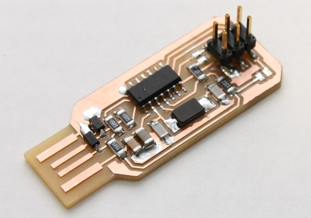
I deciced to change my Board Layout to that of Fabisp Key. It looked more decent to me especially that it looks like other memory sticks.
But again I was not able to mill my board. The tools of our Machine were all worn out and importation would take along time so I decided to use etching process eventhough Neil really discouraged usage of chemicals
This was never a challenge at all.
Despite that use of chemicals are seriously discouraged due to life threatening effects they have and encouragement of making and using machines, I got an opportunity to learn Screen Printing Method of making PCBs. This is a very neat way of making nice PCBs even with very fine tracks. From the normal screen printing method, you skip the Developer straight to Etchant/ This equally reduce the mount of chemical exposure.From the etchant, just wash your board with water, ry it and wipe away the paint you printed on it using a reducer
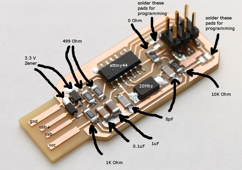
Using the above Layout which was well named, I could easily identify where each component should be soldered
I decided to smear a small layer of the Solder Paste on my board thereafter one by one layed the components starting with the centre outwards and larger ones. To be specific started I soldered ATtiny44A Microcontroller then followed by others. I would use Pick & Place Machine or other means but chose to solder directly for practice. This took me some time due to smaller size of components.
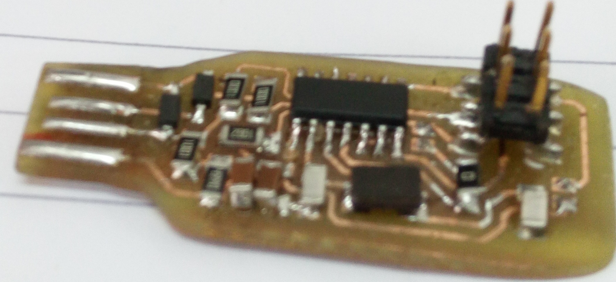
Soldering was done perfectly well.
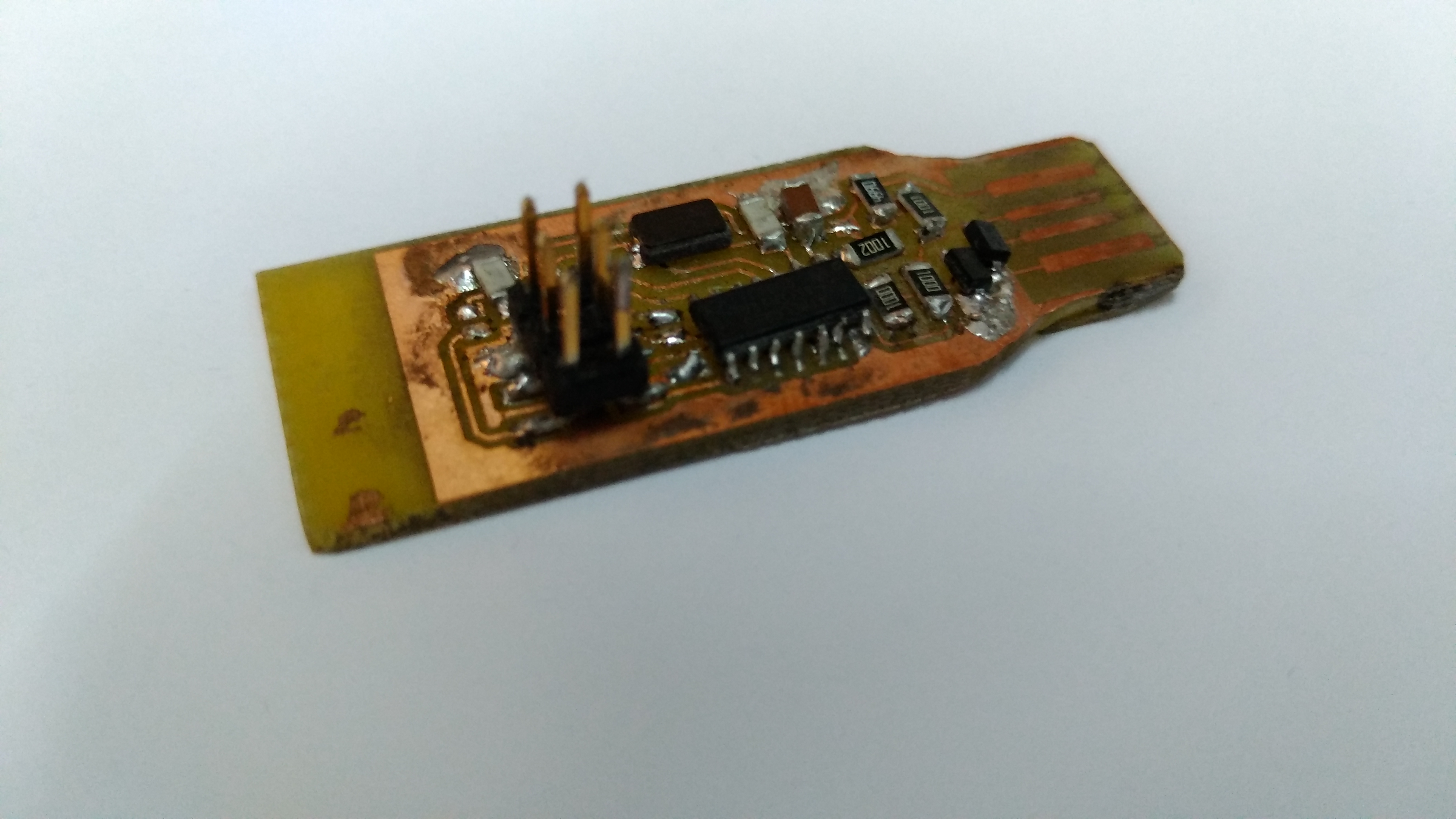
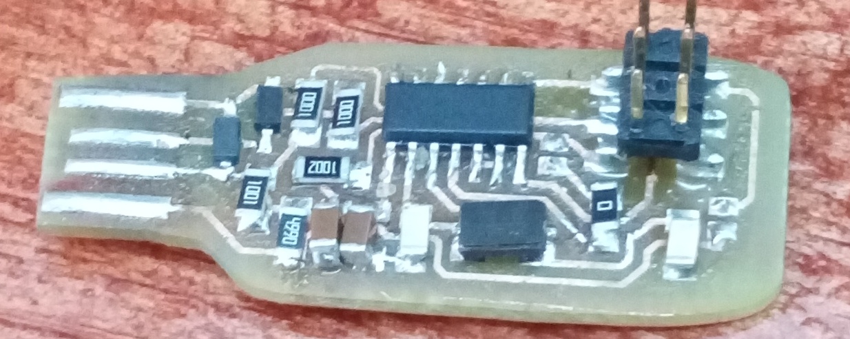
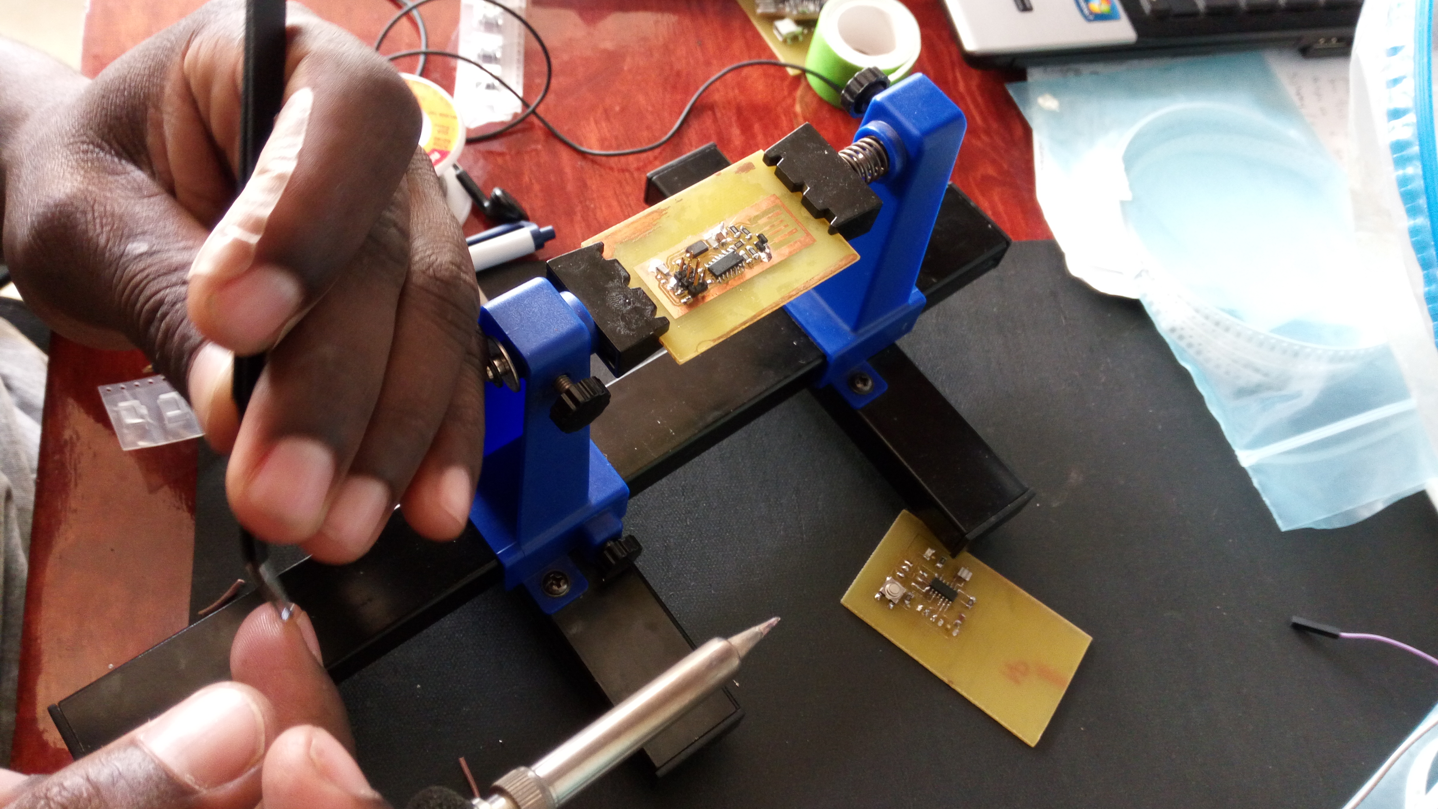
On completion, I then ran a contuinity test using a multimetre .The test was very successful
In connecting the Fabisp Key into the computer, it did not work immediately and I had to retest and troubleshoot it. I also had to fabricate the thickness of part of the board making USB in order to fit into the USB port.
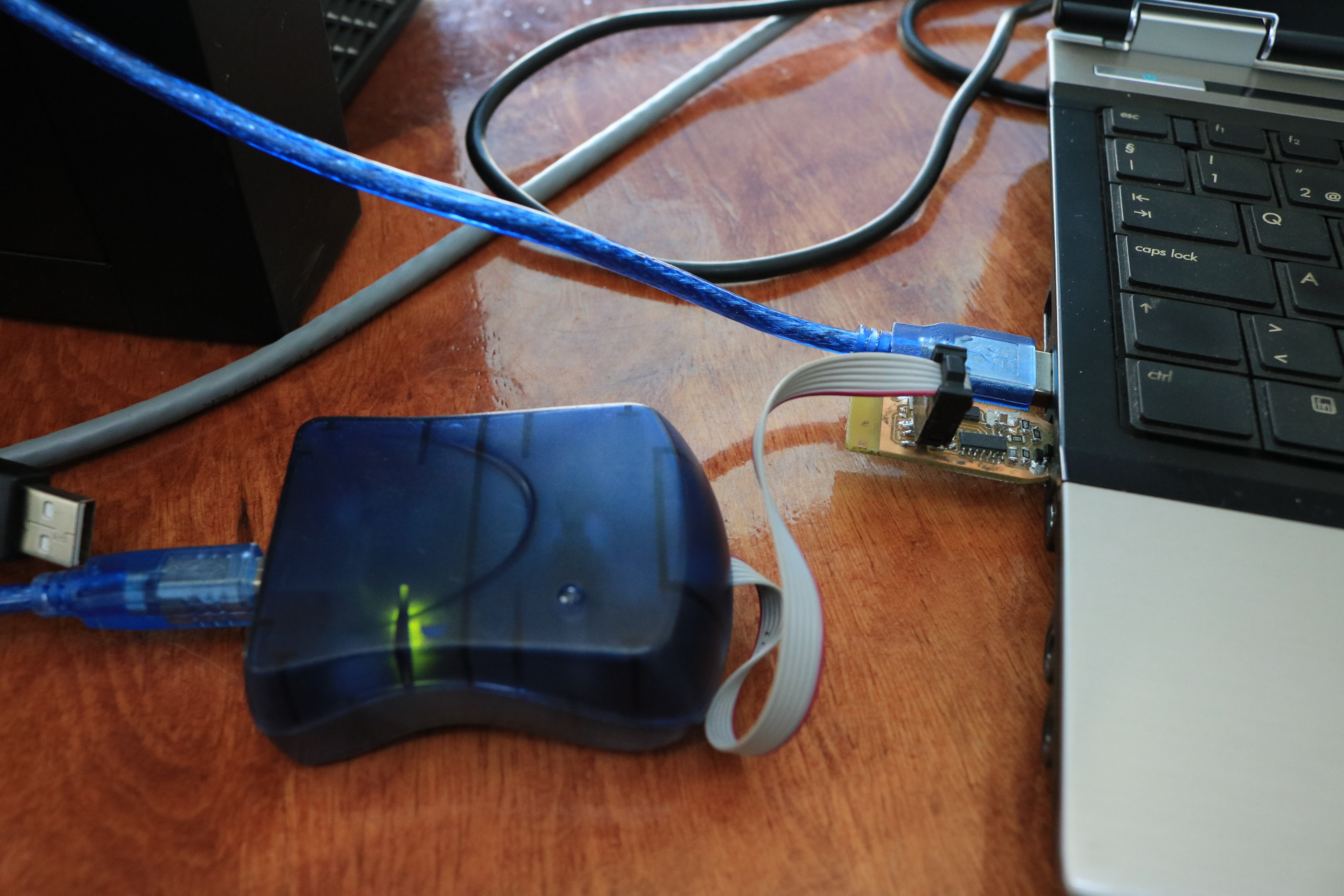
I used AVR Programmer to programme it and this was fast enough. But again, the computer continued to give a message of device not recognized. Later on after consultations, I realized that I had not removed the jumpers but when I did so, it worked. Now this board is ready to be used as a programmer to program other boards
Tutorial