Machines used and softs:
Final Objective
Redraw the echo-worl
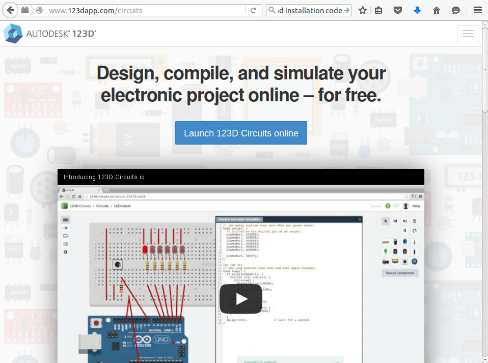
Workflow with 123D circuit from Autodesk
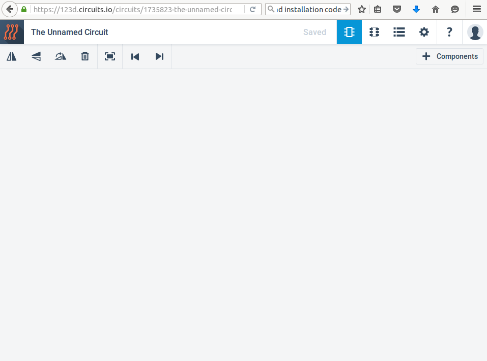
I created an account, and started a new PCB schematic:
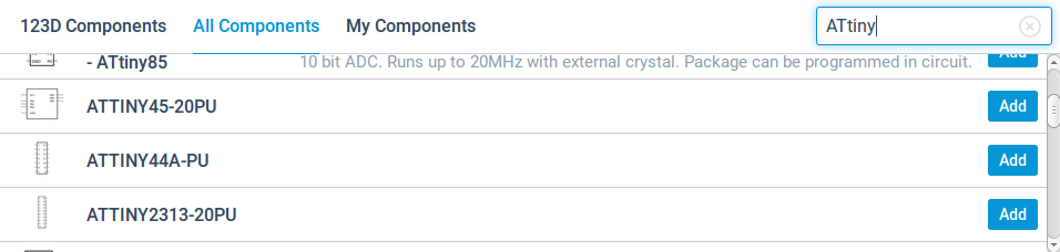
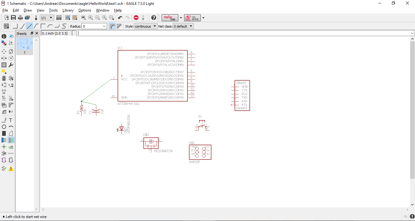
With the parts list on one side, I added all the components of the circuit, I was able to find the ATtiny 44A in the "All the components":
Here I layed down all the components that we need:
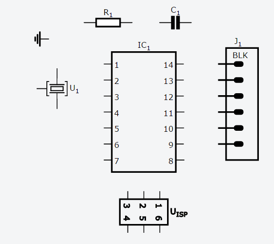
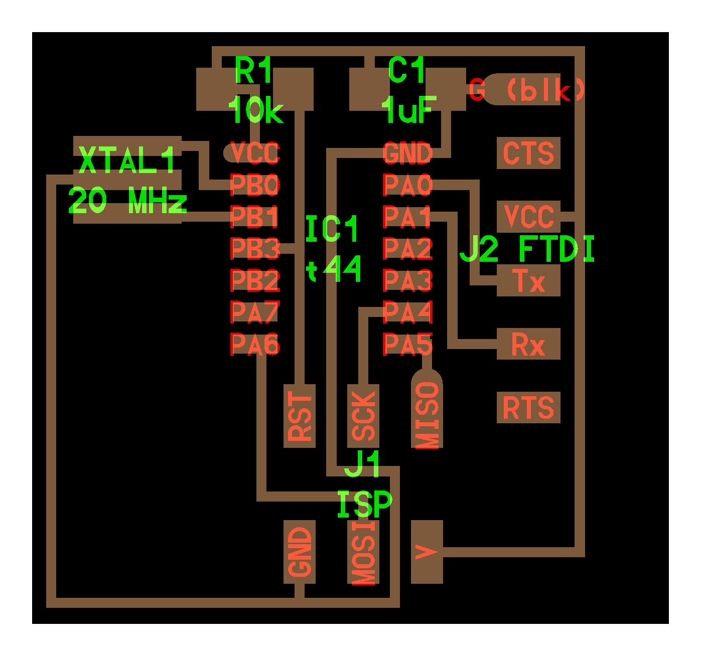
I then used the png from Neil to see how the components were connected :
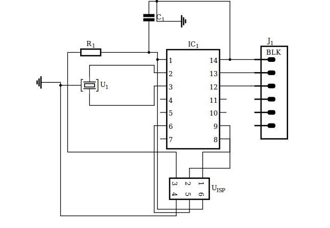
I took some time to look at the schematic and understand the role of each component, and got my final circuit:
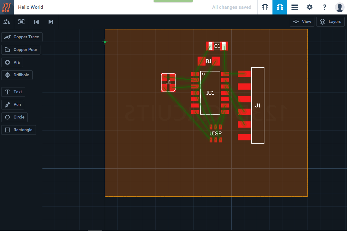
Once I was done I switched to PCB view
A new window pops we can see all the components stacked on the left top corner of the screen, let's start by cleaning this mess:
Once everything is in place , it is time to play Tetris and connect the traces!
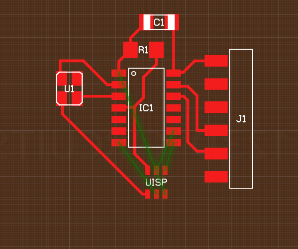
Since we are working with a single layer PCB we need to prevent tracks from overlapping on the final job.
This is why I've got trces passing underneath the ATtiny chip.
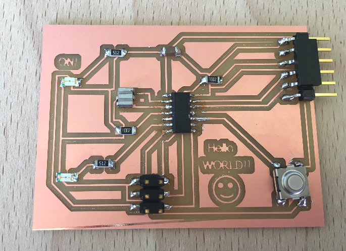
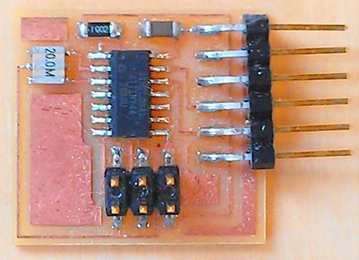
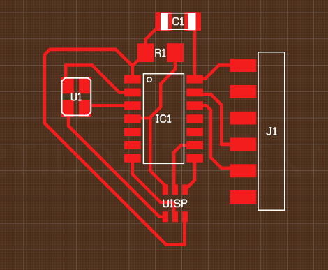
Here is my final circuit:
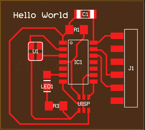
And then I added a LED and a resistor to the circuit:
I finaly imported the Gerber file :
Workflow with EAGLE

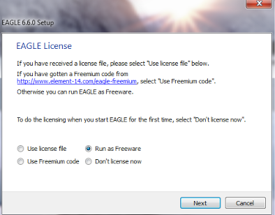
I started by downloading the last version of Eagle .
Installed it on my computer on Windows, selecting "Run as Freeware".
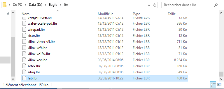
I also downloaded the fab library that contains the schematics and also the footprints of the components we will use to build the Hello World circuit.
I added the file in the main Eagle library folder EAGLE-7.5.0/lbr/ so it could be accessed without having to specify the path in the directory.
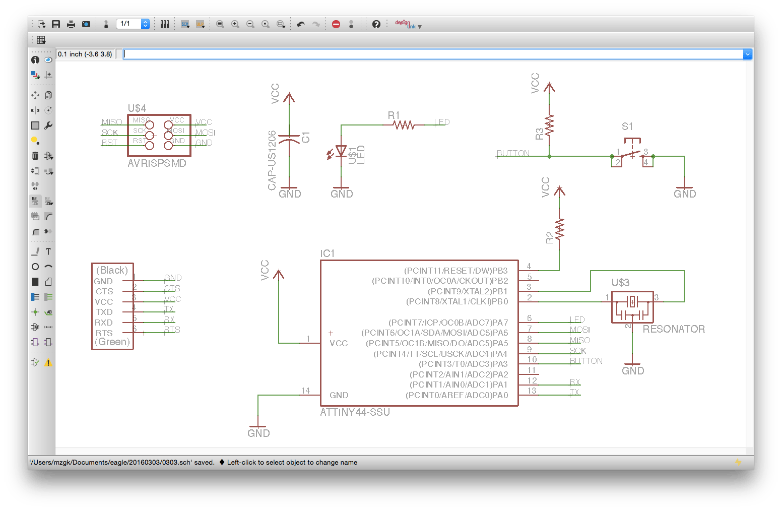
Now I am ready to design my circuit :
-create a new project : File>New>Project
-create a new schematic whitin that project : File>New>Schematic
-start adding the components : Edit>Add ...
-quit the process pressing ESC
If you didn't add the library in the Eagle directory, you can add them from the Control Pannel (Right click>Add to schematic):
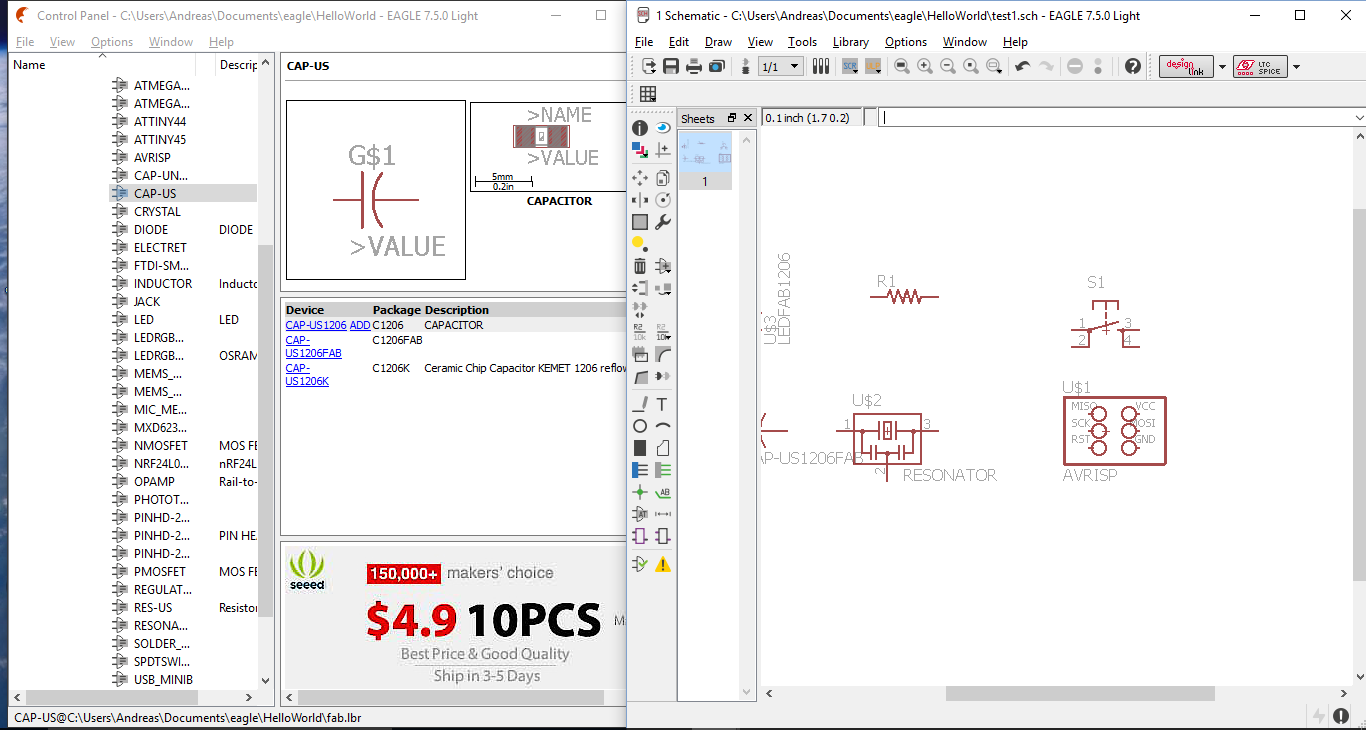
Here is the list of the components:
- ATTINY44>ATTINY44-SSU
- 6MM_SWITCH6MM_SWITCH
- AVRISP>AVRISPMD (J1-ISP)
- CAP-US> CAP-US1206FAB (C1-1uF)
- FDTI-SMD-HEADER (J2-FTDI)
- LED>LEDFAB1206 (LED1206)
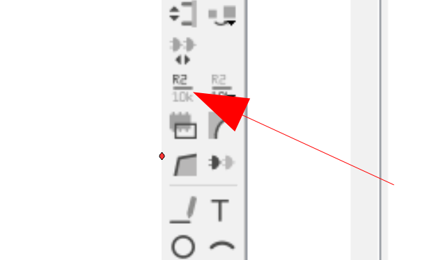
- RES-US>RES-US1206FAB (R1 10k)
- RESONATOR (XTAL 1 - 20MHZ - EFOBM)
Once all the components of the circuit habe been added, we can start wiring using the "net tool" not the "wire tool" (wire tool is free of constraints).
Simply click from a connection to another, quit by pressing ESC.
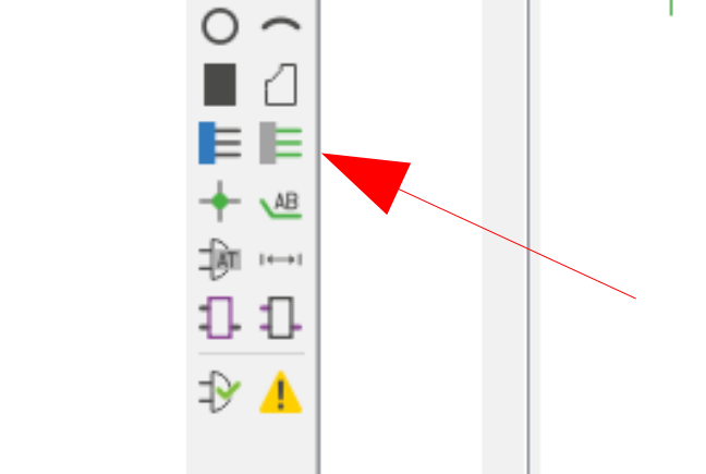
If you want to prevent having cables everywhere you can connect the nets using there names:
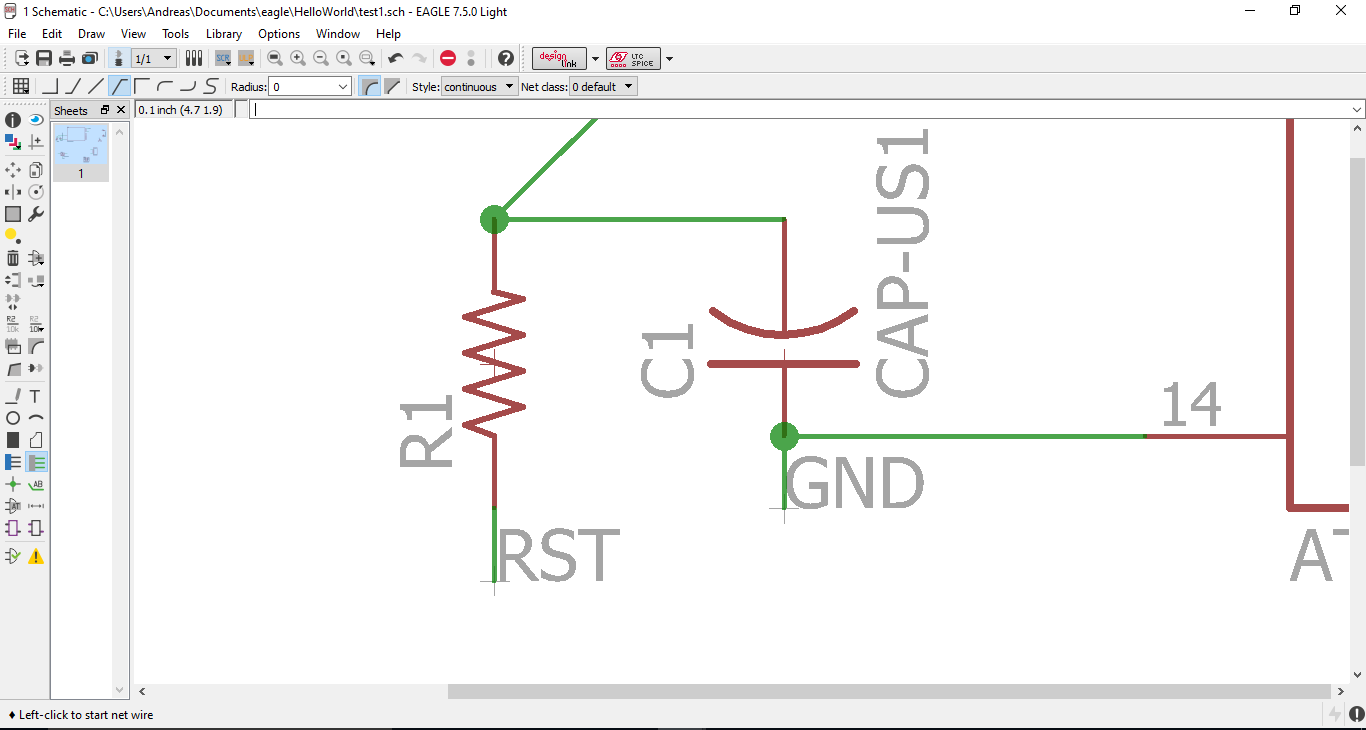
This is done by first adding a small segment of wire to each pin (it won't work if you don't do this) and then using the "name tool" :
Give the same name to each net you want to connect.
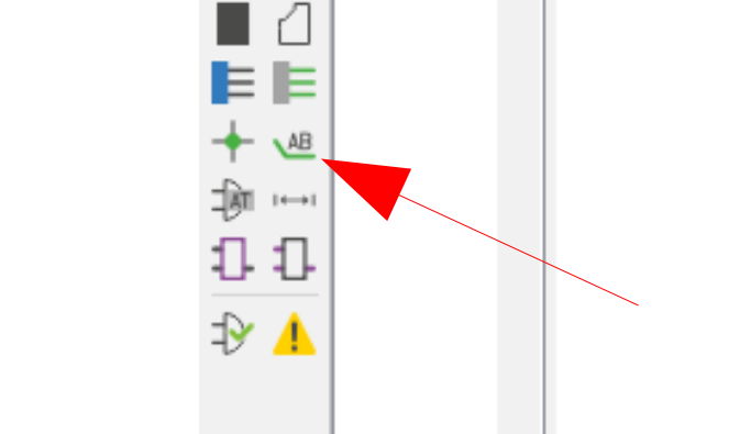
In order to remember what net you connected, you can make them visible using the "label tool":
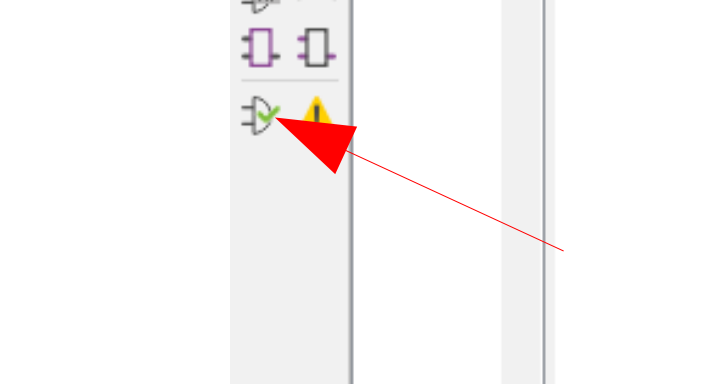
Once all the wires are connected, we need to check the schematic, click on ERC:
It is normal if the ERC check reveales connection problems even if your circuit seems to be OK ,to solve them simply move around the component using the move tool:
If the wire move with the component, everything is find, if not ,simply delete the wire that causes the issue and re-wire the component.
Once the ERC test has been passed, we can move on to the next step, the board layout:File>Switch to board .
All you components are smashed together in the left part of your screen, this is completly normal.
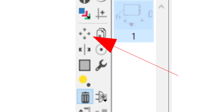
Use the "group tool" to select them all and move them in the center of the square :
You can start placing the components trying to avoid lines from crossing (rotate a component with a right click).
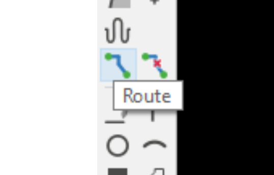
Once you have done you best, you can start playing Snake and draw the traces using the Route tool :
I used the grid (0.025'') and the wire bend style 1 and a track width of 0.016''.
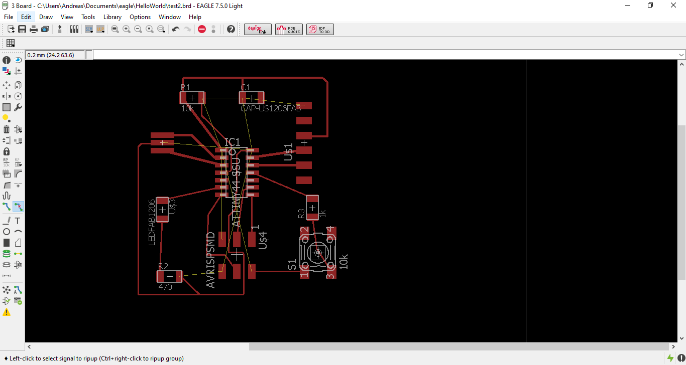
I had some trouble to avoid lines from overlapping, so I had to create a trace for my GND passing all around my board.
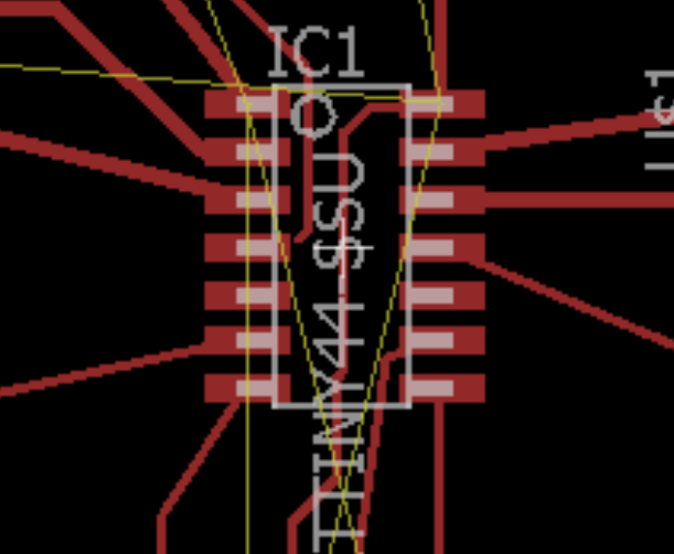
And I still had to pass some traces under the ATtiny chip
So I reduced the grid size (0.0125'' ) to position the tracks more precisely, and I also decreased the size of the wires passing under the chip.
This is my result for the moment:
There shoudn't be anymore yellow lines, but this is because I added my GND trace externaly and didn't modifie the schematic accordingly.
I am going to try to use other softwares and then I will redraw this circuit, I am not satisfied with this result.
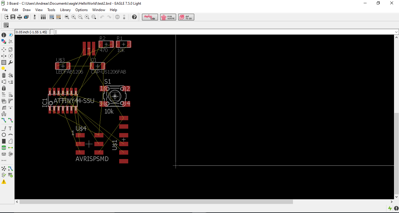
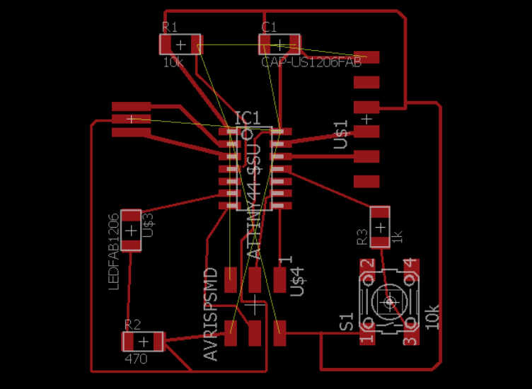
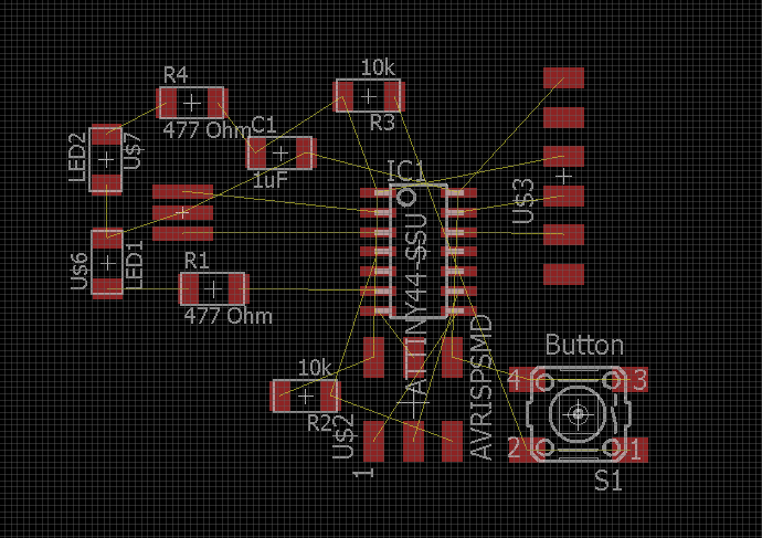
Finally I decided to stay on Eagle, so I just errased everything and re-started from scratch.
Layed down all my components:
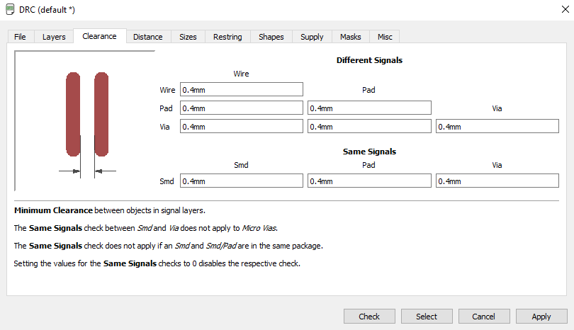
This time I properly configured the DRC:
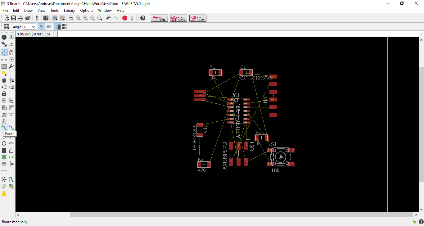
And switched to the board :
And this time I used the Autorouter tool:
I then exported my circuit in .png and using the option "Monochrome".
On one side I exported the traces (hiding all the other layers), and then exported the dimensions (which correspond to layer 20 on EAGLE).
Here are the files :
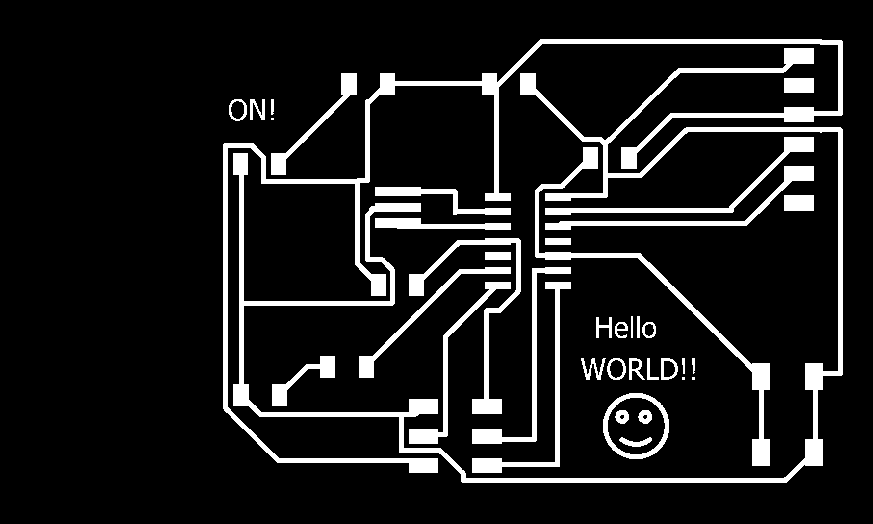

(I always get this weird offset, didn't manage to get rid of it yet!)
Next step is tho use the Fabmodules to convert those png in Gcode for the Job.
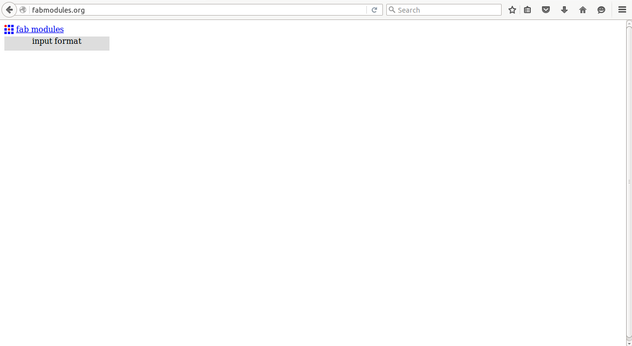
Using the Fabmodules
Fabmodules is a web site created by Neil which allows us to easily switch from a format to another in order to send a job to a machine.
Almost all the machines of the Fab inventory are already compatible !
So first we need to go on the webpage :
Select the input file:
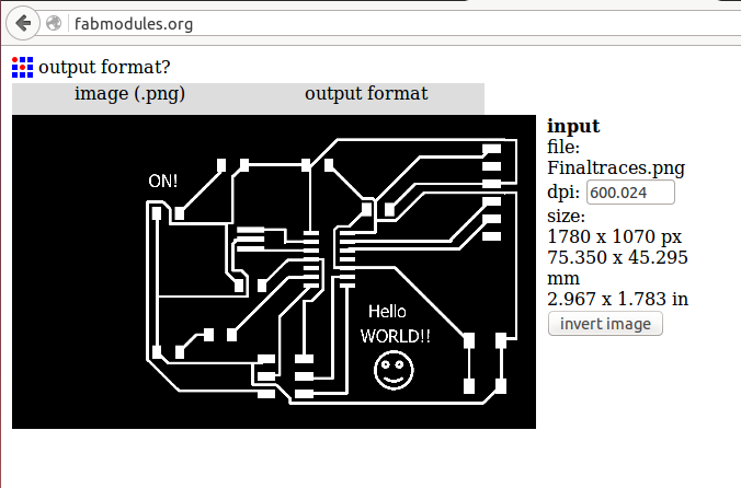
And the output file :
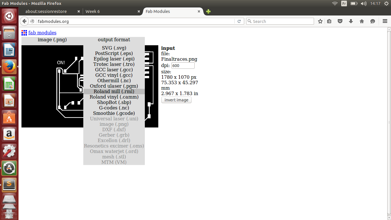
We need to precise the process ( in this case we start with the traces) :
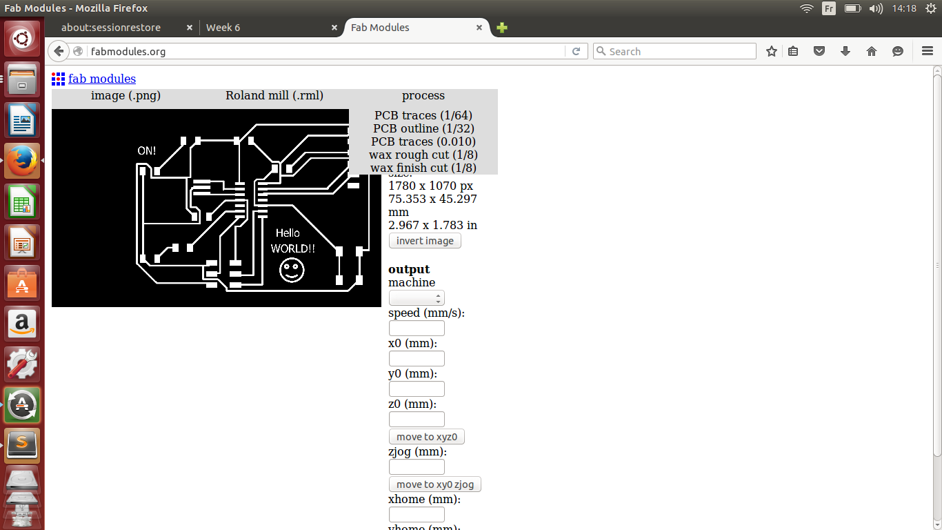
And enter some parameters for the machine:
Do not enter 0 for zhome! This will ruin your board! If we enter 0 the machine will scratch the board when homing!
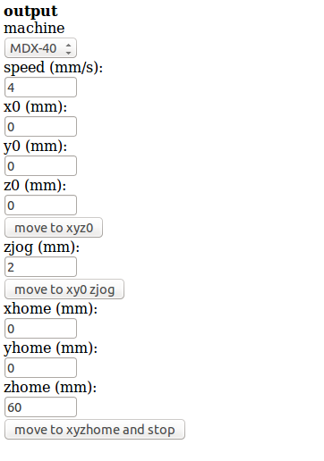
Once your done, calculate the parcour and save it!
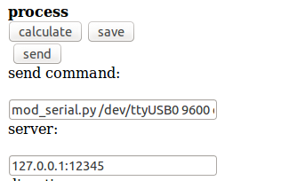
What I obtain is a Gcode that I can directly send to the MDX40:
Then I just oppended Vpanel for the Mandela machine, did my Z with a mutlimeter, and Cut!
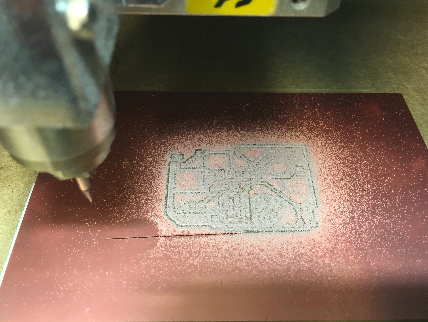
You can see the mistake I was talking about, as the machine homed at the end of the job, it scratched all the way! I'm lucky she ended there!
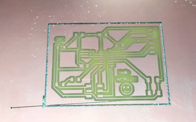
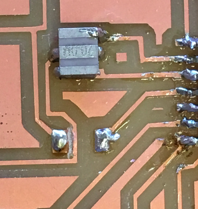
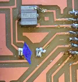
I then checked all the traces with a multimeter to insure that they were continuous.