WEEK|06
Electronic Design
For this week's assignments, we have to modify a board or design it from scratch using electronic CAD softwares. I decided to name this board Corsicaduino, because Corsica.
Software used
- KiCAD
- Eagle
Source files
Did I do that elsewhere ?
Here is the assignements where I had to use these skills :
Which tools ?

Software side
I know I already said that before, but again, I really don't like Eagle software, even if its a great tool, their stupid board size limitation makes me upset. For some time now, I used to use KiCAD less ergonomic than Eagle but it's a Free Software, and for me, this is important. Since the
CERN is involved in the project KiCAD has made hudge progress, and since version 4.0+, he's way more convenient than before, even if there's still a lot of weirdness in his workflow.
There are other electronic CAD software out there, but for the hobbyists, KiCAD is IMHO a good choice.
Yes, that was a copy/past from week 4, important things needs to be repeated often :-)
My goals
I decided to make a variant of the Barduino board that I would use for my final project as a hand controller.
The goal will be to :
- Redesign the board using KiCAD
- Adding I2C interfaces on pin 27 and 28 (replacing A4 and A5) + pullup resistors
Try todesign a keypad using parallel => I2C convertor chip, like PCF8574A on a different board (Done during project developpement)- Same thing for a LCD screen (maybe I'll use an already made LCD backpack from Adafruit) (done, too)
- Read (maybe write, too) an SD Card using I2C
How I made it
My first try was to export Schematics and PCB from Eagle to KiCAD using those scripts
 That was a incredible mess.
The tool runs several ULP scripts sequentially, each one convertying something into KiCAD format. After all the scripts has run, we have a complete KiCAD project in the target directory.
However, when I opened it, the schematics was tiny, very messy, almost all the wires wasn't properly connected...
This had been required a lots of efforts and time to clean this crap.
Plan B

So, I printed the schematics, done some anotation on it for the modifications I wanted to make, and restarted from scratch with eeSchema.
No real problem for this step, this was done relatively fast, and then comes the time where we need to associate footprints to components using CvPcb.
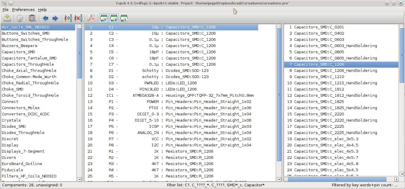
This isn't a hard part on its own, but sometime it's a bit tricky, because as powerfull KiCAD is, it still lacks some coherence in his parts library / modules, and the ergonomy of CvPcb needs to be more intuitive and less buggy.
Anyway, with some time wasted finding the right footprint in a few meters long list, all parts had their footprint and the netlist was ready to be generated.
Netlist generation is as simple as clicking on the "NET" button and click "Generate" (and saying that loudly with a Dalek voice is funny, nevermind).
This needs to be done after the footprint association - I say that because in older version of KiCAD, netlist needed to be generated before AND after footprint association, first into eeschma, then into CvPcb. That's an improvement.
When the netlist is generated, we can switch to pcbnew to import it and begin the placement of the components. And this is a really boring task.

I hadn't any strict constrain about the board size (just not too big because this is for a handheld controller), so I begun with 5cm squared board size, and this was finally almost OK (still a little to big, final size is 50x41mm)
One of my concern was about the track size and clearance, as my previous attempt to make a PCB resulted in a totally unusable board
So, at first, I goes to "design rules" and sets clearance and minimum track size of 0.4mm, the diameter of the endmill.
Of course, it would've been to easy. Setting a clearance of 0,4mm avoided me to draw any tracks on the pads of the ATMega168 (TQFT32 package). As this is a central component, I cannot say to KiCAD to simply uses a 0,3mm clearance only on his pads, so I ended up with a 0.3 clearance by default, trying keep 0.4 manually as most as I could.
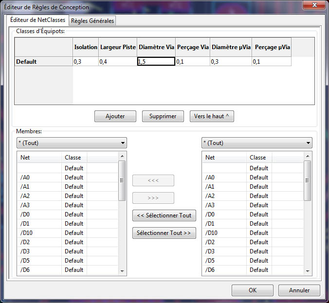
As I'd known I would have to do some bridges to jump over tracks, I also setted via's diameter to 1.5mm and via holes to 0.1mm (because vias needs a hole), so this gave me some nice pads where I will solder some insulated wires.
When I associated footprints to components, I used classic pin-headers (with throuh-hole pads) because they was'nt any SMD pin headers available. So I had to manually change all the pads on this pin-headers to make them SMD. This is easy doable by typing "E" with cursor over a pad, but it's booooring...
About that, KiCAD manages this in a pretty good way (IMHO) : we don't have to neither modify the footprint in the librairy nor create a new librairy for that.
Instead, KiCAD uses a cache-file for the footprints in a project. This allows to use a pretty standard footprint and just do some adjustments on it, on a per-project basis. If we share the project (with all its files), this customized footprints would be available without the need to import something.
Of course, if a customized footprint will be used frequently on a large number of project, it is best to make a librairy. And as KiCAD support GIT repos as libraries, it could be very powerfull.
Once the board design was completed (it took me 7 hours... Wow), I used Fabmodules the same way as for Week 4 with just two things witch I was especially careful :
- DO NOT forget to invert image
- Carefully check if traces wasn't fused
The workaround I used was a bit tricky... I simply set the tool size to 0.3mm, knowing that is would eat a little more part of tracks and pads, but doing this allowed me to get a clean board.

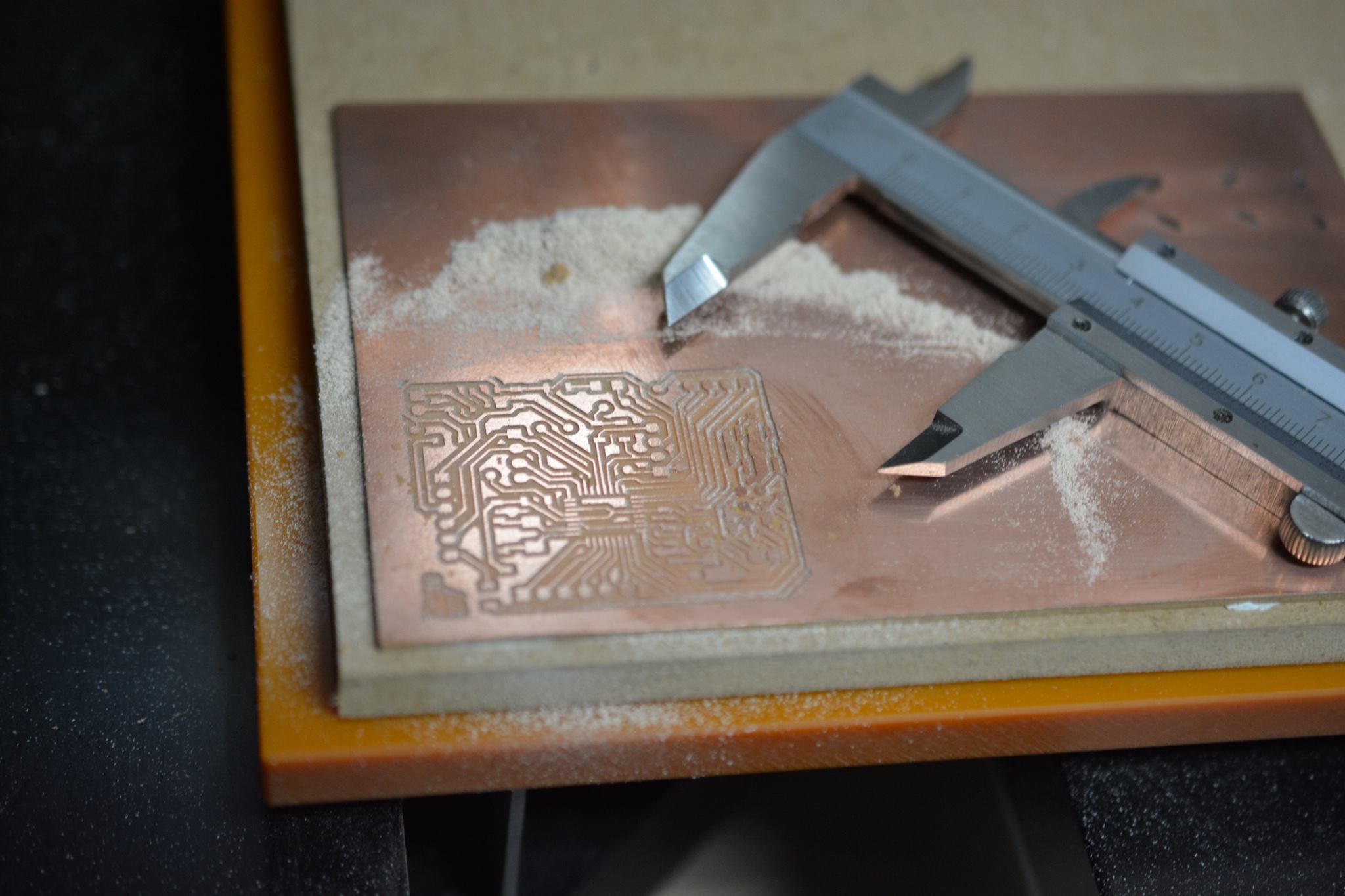
As we can imagine, traces are a bit thinner than designed, but with a bit of patience, a good magnifier and a very steady hand, I think it should be OK.
However, this time the endmill engraved more deeply in the FR1 than the last week. That's weird because the copper board and fabmodules settings was exactly the same (except for tool diameter and 2 other settings not related), as was the initialization of the MDX-40.
Even if this is not really a problem, I need to investigate why there was so much difference. Maybe the board wasn't totally flat, but that would surprise me.
Anticipating
Next week, I will be very busy at work, so I know that I could not come to the fablab until friday 18th... I hope to finish the board in time.
Soldering the board
The busy week is over, so I can focus on soldering all the components
All went fine, until I came to the straps and headers. This was heavy, because headers have corner-angle pin and I did not choose the right footprint on my PCB. So with the help of pliers, I straightened the pin and soldered them. It's ugly, it's not mechanically strong, but the contacts are good and without shorts, so for me it's OK.
Wires running over the board was made to make easier the routing, but it's a pain in the ass to do a clean work with all that spaghetti-like mess, next time I'll try to reduce as most as possible this workaround.
Testing the board
With my FabISP (wich is working, it was used to program my colleagues others FabISP on Week4), it didn't work at all, but with the AVRISP MkII, All was OK !?
$ sudo avrdude -c avrisp2 -p m328p

avrdude: AVR device initialized and ready to accept instructions

Reading | ################################################## | 100% 0.01s

avrdude: Device signature = 0x1e950f

avrdude: safemode: Fuses OK (E:07, H:D9, L:62)

avrdude done.  Thank you.
$ sudo avrdude -c usbtiny -p m328p
avrdude: Error: Could not find USBtiny device (0x1781/0xc9f)


avrdude done.  Thank you.

!!!!!!!! OOPS - forgot to plug-in the FabISP :D !!!!!!!!

$ sudo avrdude -c usbtiny -p m328p

avrdude: initialization failed, rc=-1
         Double check connections and try again, or use -F to override
         this check.


avrdude done.  Thank you.
Weird, but as the board is working with at least a programmer, I will investigate this problem later (may be on week 8)
After investigation, it turns out that the ICSP connector on the FabISP was inverted ! Just had to invert it and voilà !
My mistakes
Surprisingly, I didn't seem to make any mistakes this week. But I'll wait until the board is fully soldered before claiming for victory.
So, except the weird thing with my FabISP (more on that on Week8), all was OK, so I can say that I made no real mistakes this week, Yohohoo \o/
Anyway, like I said before, using lots of VIAs is time-consuming for soldering, and I need to think about the right footprint for the components available in the fablab BEFORE engraving my board.