Drawing the Board
I decided to get stuck in using 123D Circuits as I’ve already used some of the other apps from the 123D family - they are usually a good starting point for beginners. I got right to it and chucked components into the schematic view, then linked them up.
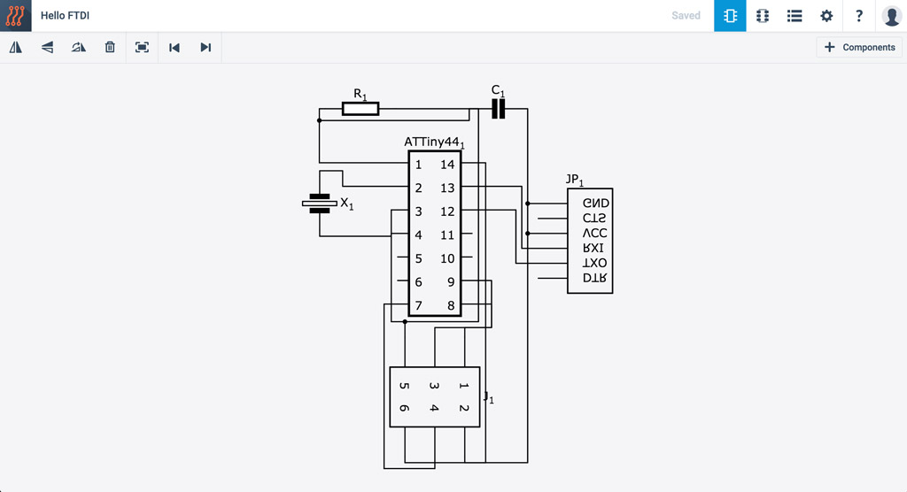 My first stab at a schematic for the Hello Echo board
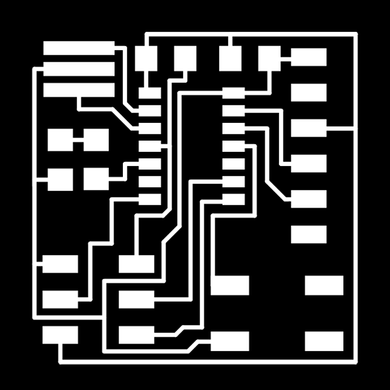
I switched to PCB View and started laying out and routing the components and traces.
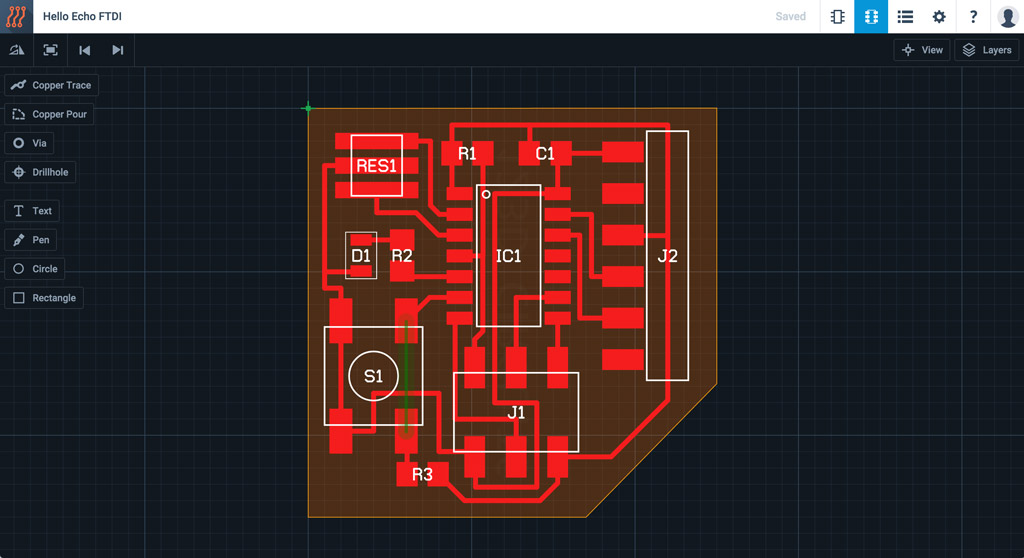
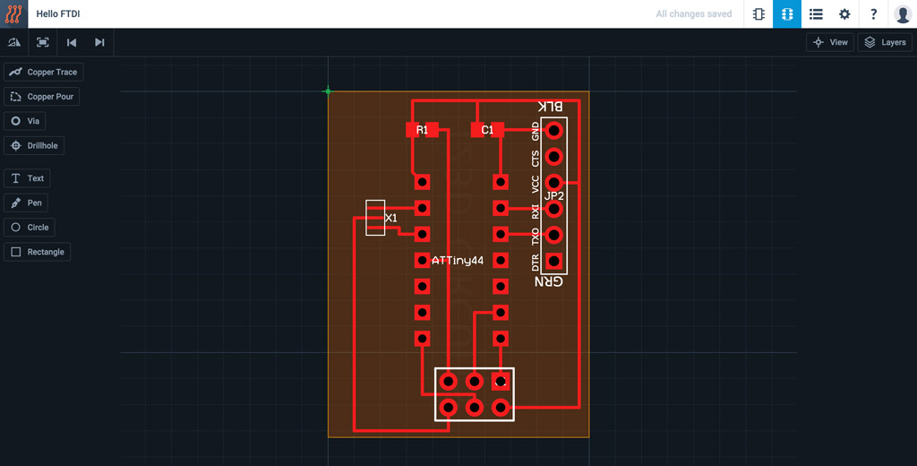 Components places and traces routed (almost)
Getting the traces right took a few attempts. I jumped backwards and forwards between the Schematic View and PCB View until I had almost everything connected correctly.
It was at that point I realised that I didn’t have enough space for the trace between pin 14 (GND) on the ATtiny44 to pass under the 2x3-pin header. This was a symptom of a bigger problem - I had through-mount versions of the headers and ATtiny!
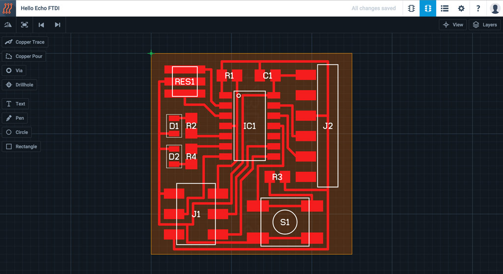
 Comparison between my Hello Echo board and the original (through-mount components highlighted)
The footprint of the crystal also looked wrong, so I decided to start creating my own components to add to the 123D library.
Making new components in 123D Circuits is quite straight-forward, but there are one or two quirks to watch out for. First of all, once you have completed your schematic symbol, footprint and terminal mapping, you need to go to the component overview and ‘Mark as Done’ before it becomes available in your component library.
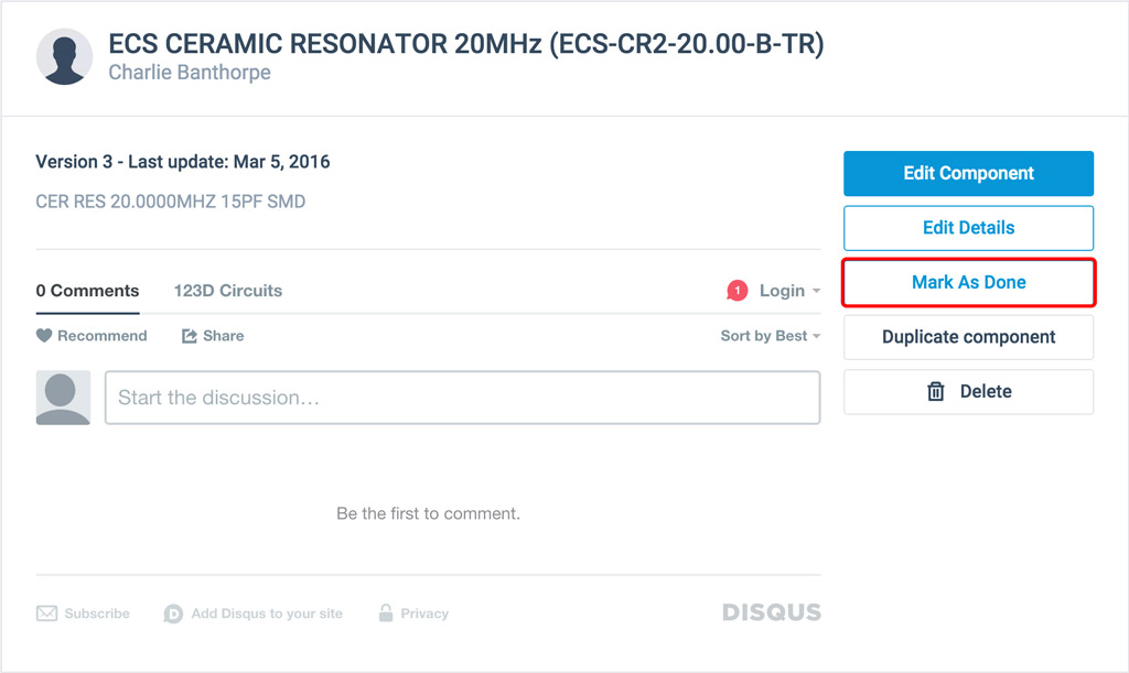 Mark your components as done to add them to your library
It’s also worth noting that if you make edits to a component after it’s been added to a PCB design, you must again ‘Mark as Done’, delete the old component from your schematic and add in the new component again.
Not the smoothest workflow for iterative design!
After creating components for the ATtiny44, resonator, 6x1-pin header, 3x2-pin header and tactile button, I switched back to the design to tidy up the schematic and board layout then add the LED and tactile switch.
 The board with LED and tactile switch added, traces getting tangled
I looked at Lisa Schlecht’s Embedded Programming documentation for pointers on connecting the LED and switch. After a few iterations, I managed to untangle the traces. Since I had the space, I also added a second LED.
 Traces traced and second LED added
Milling the Board
The design can be downloaded directly from 123D Circuits in Gerber format.
Most graphics editing packages will not read Gerber files, so you’ll need a Gerber viewer/converter to get the designs into PNG format ready to feed into Fab Modules - I used circuitpeople.com.
Once I had the PNGs I used Photoshop to invert the image, check the resolution vs. physical dimensions then added a 30px margin on all sides to allow for the board cutout (the 1/32” tool used for the cutout equates to 15.625 pixels at 500 dpi, so a 30px margin is quite generous).
I uploaded the trace image to Fab Modules, tuning the path error parameter down to 0.8 to smooth the toolpaths and the number of offsets to -1 to mill out all the excess copper. Milling out the excess copper is not necessary, takes longer and wears the tool more than necessary…
But I did it anyway, because I think it looks better!
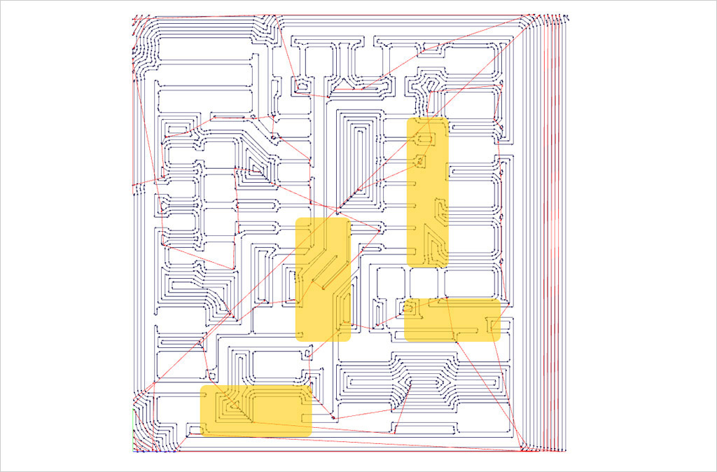 Toolpath in Fab Modules with troublesome areas highlighted
Some of my traces were too close together and not separated, so I made one more iteration then milled the board with the MDX-20.
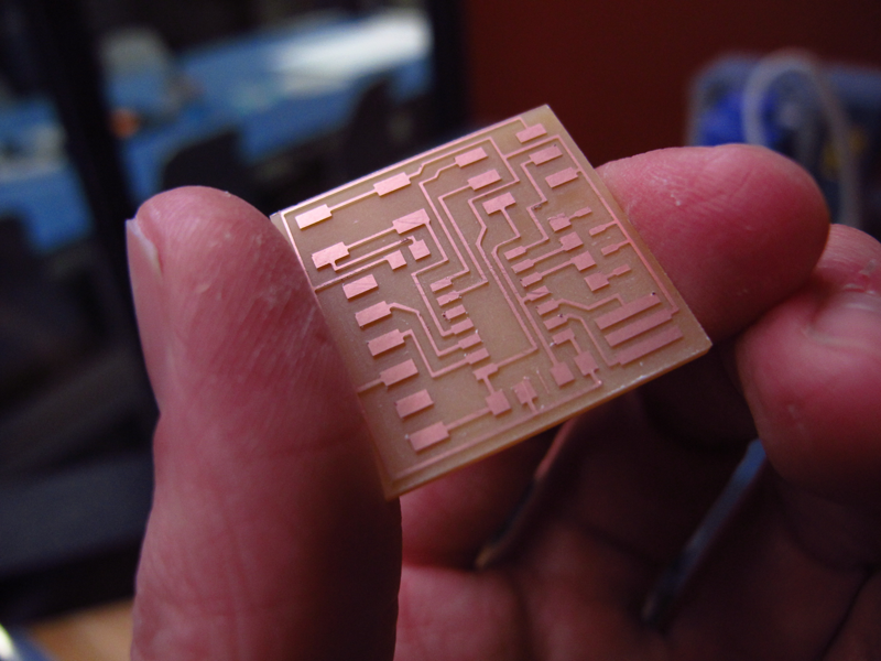 Traces milled and the board cut out
*Full disclosure - I broke the endmill on my first attempt due to vibrations at the tool tip. For the second try, I set the tool much deeper in the chuck and double checked the tightness of the set screw.
Stuffing the Board
I gathered the components and got set up to stuff the board. We only have the articulated-magnifying-man type of helping hands in our Lab. I wanted something a bit more sturdy, so I improvised something like a Panavise from a quick clamp and a bench vise.
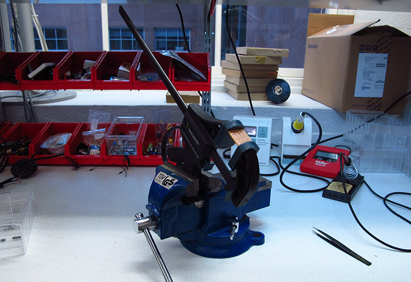 Sometimes you’ve just gotta improvise!
I soldered the ATtiny44 first, then moved on to the resistors. These proved almost impossible to solder because I had made the footprints too small!
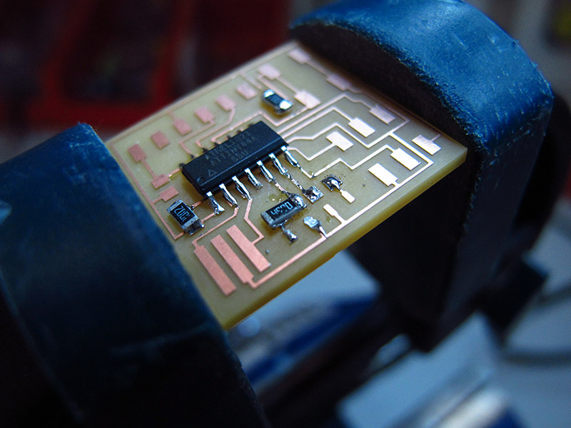 The footprints were too small, but I had a bash at it anyways
Back to 123D Circuits once more to change the resistors and capacitor to ‘1206’ footprints. I also removed the second LED to give myself a bit more elbow room.
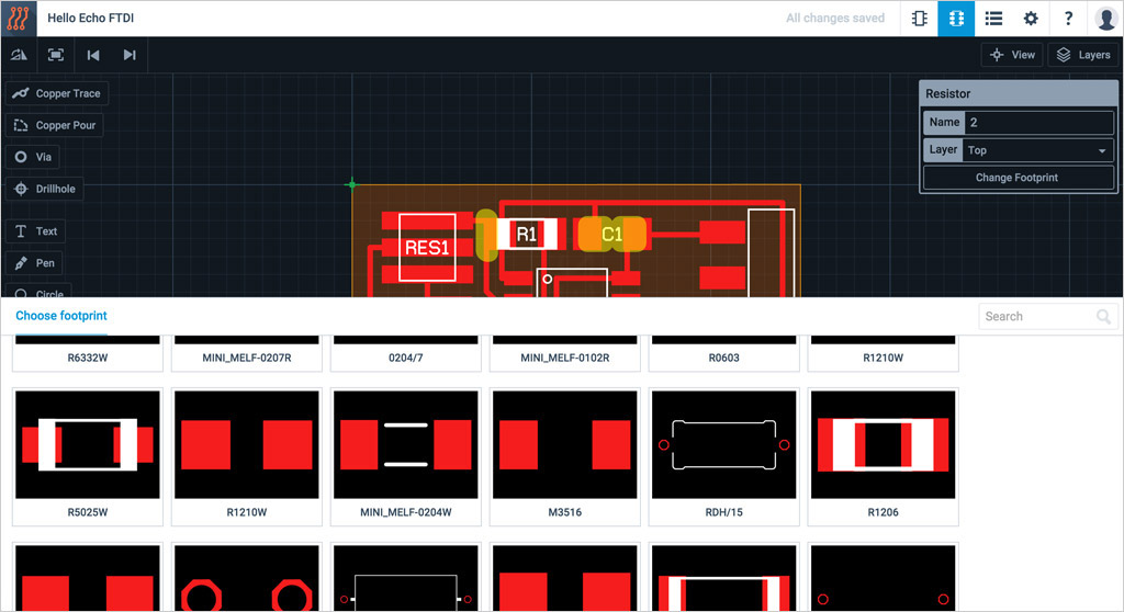 Switching to 1206 footprints for resistors and the capacitor
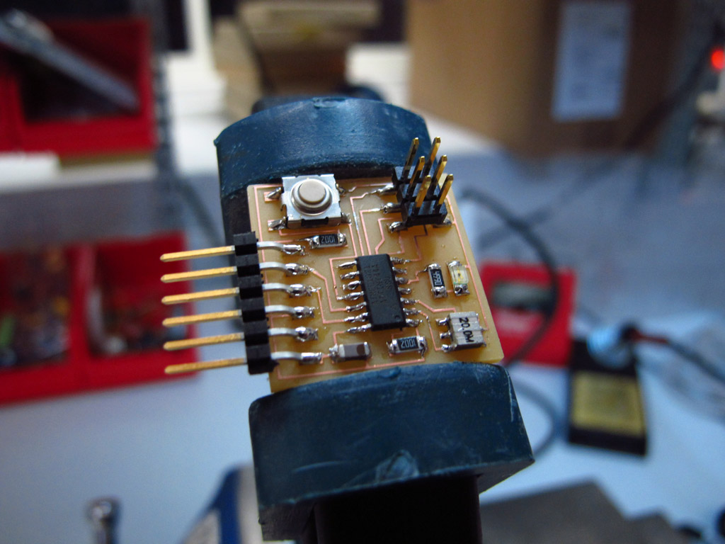 The new board milled, stuffed, signed, sealed and delivered
Design Rules Check (DRC)
123D Circuits doesn’t currently expose the design rules to the user within the application for viewing or customizing. After a quick search in their community pages, I found this article: PCB fabrication design rules and DRC errors which lists the default design rules.
Crucially, the space between traces must not be less than 6mil (0.1524mm) according to the design rules. This is a problem when using a 1/64” (0.4mm) endmill for milling traces, which is larger than the 6mil limit. This explains why some of my traces were not separated in the Fab Modules toolpaths, but passed the 123D Circuits DRC.
I have submitted a feature request to Autodesk to allow custom design rules to be set.
Further Improvements
After reviewing my board design with our remote guru Bas, I made a few amendments:
- R3 is not necessary as internal pull-up resistors can be assigned individual ATtiny44 pins.
- Traces between the legs of the tactile switch are not necessary because they are routed internally (obviously!).
I used a knife to cut the traces leading to and from R3, and left the traces below the button as an eternal mistake! This was a good lesson for me about not following other people’s documentation with out digging deep enough to understand exactly why things have been done the way they have been done…
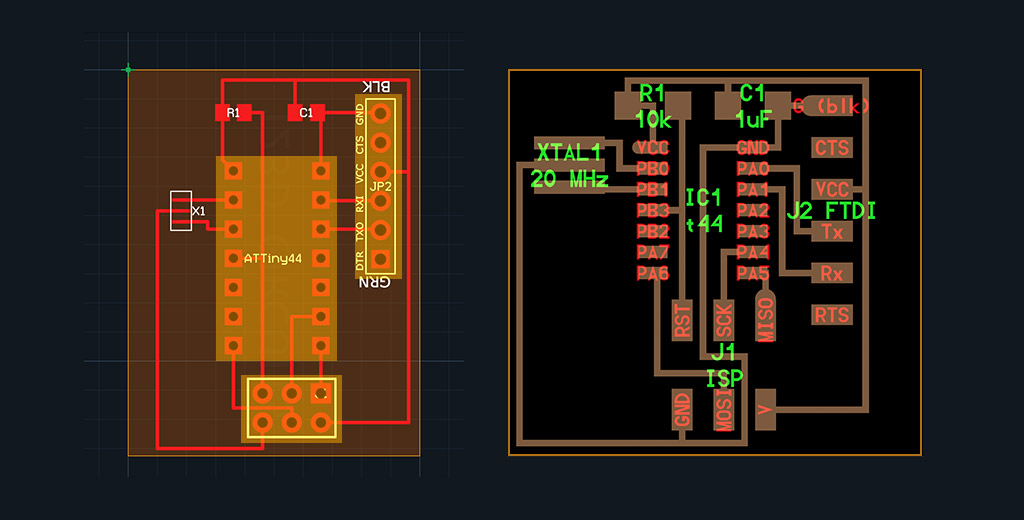
Here’s the final schematic, PCB layout and bill of materials:
Files
Gerber (34kB) - helloecho-gerber.zip
Traces (500dpi, 2kB) - helloecho-traces.png
Cutout (500dpi, 15kB) - helloecho-cutout.png
TODOs
☑ Redraw the echo hello-world board
☑ Add a button and LED with current-limiting resistor
☑ Explain problems and solutions
☑ Do fabbercise
☑ Include original design files
Links
Fab Academy 2016 - Electronics Design
Project on 123D Circuits - Hello Echo FTDI